 | –≠–ª–µ–∫—Ç—Ä–æ–Ω–Ω—ã–π –∫–æ–º–ø–æ–Ω–µ–Ω—Ç: CY28404OC | –°–∫–∞—á–∞—Ç—å:  PDF PDF  ZIP ZIP |
CK409-Compliant Clock Synthesizer
CY28404
Cypress Semiconductor Corporation
∑
3901 North First Street
∑
San Jose
,
CA 95134
∑
408-943-2600
Document #: 38-07510 Rev. *B
Revised June 16, 2004
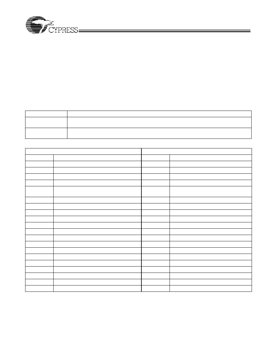
Features
∑ Supports Intel
Springdale/Prescott (CK409)
∑ Selectable CPU frequencies
∑ 3.3V power supply
∑ Nine copies of PCI clock
∑ Four copies 3V66 clock with optional VCH
∑ Three copies 48-MHz clock
∑ Three copies REF clock
∑ Two differential CPU clock pairs
∑ Support SMBus/I
2
C Byte, Word, and Block Read/Write
∑ Dial-A-Frequency
∑ Ideal Lexmark Spread Spectrum profile for maximum
electromagnetic interference (EMI) reduction
∑ 48-pin SSOP package
Table 1. Frequency Table
CPU
3V66
PCI
REF
48M
x 2
x 4
x 9
x 3
x 3
Block Diagram
Pin Configuration
SSOP-48
~
VDD_REF
XTAL
PLL Ref Freq
XOUT
XIN
VDD_PCI
OSC
SCLK
PLL 1
WD
Timer
VDD_48MHz
SDATA
VDD_3V66
Divider
Network
VDD_CPU
FS_(A:E)
PD#
REF(0:2)
VTT_PWRGD#
IREF
3V66_(0:2)
PCIF(0:2)
PCI(0:5)
DOT_48
3V66_3/VCH
2
PLL2
CPUT(0:1), CPUC(0:1)
USB_48
**FS_A/REF_0
**FS_B/REF_1
XIN
XOUT
VSS_REF
*FS_C/PCIF0
*FS_D/PCIF1
*FS_E/PCIF2
VDD_PCI
VSS_PCI
PCI0
PCI1
PCI2
PCI3
VDD_PCI
VSS_PCI
PCI4
PCI5
RESET#/PD#
*SEL24#/24_48MHz
DOT_48
USB_48
VSS_48
REF_2
VDDA
VDD
DNC***
DNC***
VSS
CPUT0
CPUC0
VDD_CPU
CPUT1
CPUC1
VSS_CPU
IREF
3V66_3/VCH/SELVCH**
SCLK*
SDATA*
3V66_0
VTT_PWRGD#
VSSA
VDD_3V66
3V66_2/MODE*
VDD_48
48
47
46
45
44
43
42
41
40
39
38
37
36
35
34
33
32
31
30
29
28
27
26
25
1
2
3
4
5
6
7
8
9
10
11
12
13
14
15
16
17
18
19
20
21
22
23
24
C
Y
2
840
4
VDD_REF
3V66_1
VSS_3V66
I
2
C
Logic
RESET#
** 150k Internal Pull-down
* 150k Internal Pull-up
2
24_48MHz
SELVCH
SEL24#
MODE
*** Do Not Connect
CY28404
Document #: 38-07510 Rev. *B
Page 2 of 20
Pin Description
Pin No.
Name
Type
Description
1, 2, 48
REF(0:2)
O, SE
Reference Clock. 3.3V 14.318-MHz clock output.
1, 2, 7, 8, 9
FS_A, FS_B, FS_C,
FS_D, FS_E
I
3.3V LVTTL Latched Input for CPU Frequency Selection.
4
XIN
I
Crystal Connection or External Reference Frequency Input. This pin has
dual functions. It can be used as an external 14.318-MHz crystal connection
or as an external reference frequency input.
5
XOUT
O, SE
Crystal Connection. Connection for an external 14.318-MHz crystal output.
40, 43
CPUT(0:1)
O, DIF
CPU Clock Output. Differential CPU clock outputs.
39, 42
CPUC(0:1)
O, DIF
CPU Clock Output. Differential CPU clock outputs.
37, 36
DNC
Do Not Connect
30, 31
3V66(0:1)
O, SE
66-MHz Clock Output. 3.3V 66-MHz clock from internal VCO.
26
3V66_3/VCH/
SELVCH
I/O, SE
PD
48- or 66-MHz Clock Output. 3.3V selectable through external SELVCH
strapping resistor and SMBus to be 66 MHz or 48 MHz. Default is 66 MHz.
0 = 66 MHz, 1 = 48 MHz
27
3V66_2/MODE
I/O, SE
PU
66-MHz Clock Output. 3.3V 66-MHz clock from internal VCO. Reset or
Power-down Mode Select. Selects between RESET# output or PWRDWN#
input for the PWRDWN#/RESET# pin. Default is RESET#. 0 = PD, 1 = RESET.
7, 8, 9
PCI_F(0:2)
O, SE,PU Free Running PCI Output. 33-MHz clocks divided down from 3V66.
12, 13, 14, 15,
18, 19
PCI(0:5)
O, SE
PCI Clock Output. 33-MHz clocks divided down from 3V66.
23
USB_48
O, SE
Fixed 48-MHz Clock Output.
22
DOT_48
O, SE
Fixed 48-MHz Clock Output.
45
IREF
I
Current Reference. A precision resistor is attached to this pin which is
connected to the internal current reference.
20
RESET#/PD#
I/O, PU
3.3V LVTTL Input for PowerDown# active LOW. Watchdog Time-out Reset
Output.
21
SEL24#/
24_48MHz
I/O, SE
PU
24- or 48-MHz Output. 3.3V fixed 24-MHz or 48-MHz non-spread spectrum
output selectable through an external power-on strapping resistor tied to this
pin. 0 = 24 MHz, 1 = 48 MHz
34
VTT_PWRGD#
I
3.3V LVTTL Input is a Level Sensitive Strobe used to Latch the FS[A:E]
Input (active LOW).
33
SDATA
I/O
SMBus-compatible SDATA.
32
SCLK
I
SMBus-compatible SCLOCK.
47
VDDA
PWR
3.3V Power Supply for PLL.
46
VSSA
GND
Ground for PLL.
3, 10, 16, 25,
28, 35, 41
VDD(REF,PCI,48,3
V66,CPU),
PWR
3.3V Power Supply for Outputs.
6, 11, 17, 29,
38, 44, 46
VSS(REF,PCI,48,3V
66,CPU,ITP)
GND
Ground for Outputs.
CY28404
Document #: 38-07510 Rev. *B
Page 3 of 20
MODE Select
The hardware strapping MODE input pin can be used to select
the functionality of the RESET#/PD# pin. The default (internal
pull-up) configuration is for this pin to function as a RESET#
Watchdog output. When pulled LOW during device Power-up,
the RESET#/PD# pin will be configured to function as a
Power-down input pin.
Frequency Select Pins
Host clock frequency selection is achieved by applying the
appropriate logic levels to FS_A through FS_E inputs prior to
VTT_PWRGD# assertion (as seen by the clock synthesizer).
Upon VTT_PWRGD# being sampled LOW by the clock chip
(indicating processor VTT voltage is stable), the clock chip
samples the FS_A through FS_E input values. For all logic
levels of FS_A through FS_E VTT_PWRGD# employs a
one-shot functionality in that once a valid LOW on
VTT_PWRGD# has been sampled, all further VTT_PWRGD#
and FS_A through FS_E transitions will be ignored.
Table 2. Frequency Selection Table
Input Conditions
Output Frequency
VCO Freq.
PLL Gear
Constants
(G)
FS_E
FS_D
FS_C
FS_B
FS_A
CPU
3V66
PCI
FSEL_4 FSEL_3 FSEL_2
FSEL_1
FSEL_0
0
0
0
0
0
100.7
67.1
33.6
805.6
24004009.32
0
0
0
0
1
100.2
66.8
33.4
801.6
24004009.32
0
0
0
1
0
108.0
72.0
36.0
864.0
24004009.32
0
0
0
1
1
101.2
67.5
33.7
809.6
24004009.32
0
0
1
0
0
Reserved
Reserved
Reserved
Reserved
Reserved
0
0
1
0
1
Reserved
Reserved
Reserved
Reserved
Reserved
0
0
1
1
0
Reserved
Reserved
Reserved
Reserved
Reserved
0
0
1
1
1
Reserved
Reserved
Reserved
Reserved
Reserved
0
1
0
0
0
125.7
62.9
31.4
754.2
32005345.76
0
1
0
0
1
130.3
65.1
32.6
781.6
32005345.76
0
1
0
1
0
133.6
66.8
33.4
801.6
32005345.76
0
1
0
1
1
134.2
67.1
33.6
805.2
32005345.76
0
1
1
0
0
134.5
67.3
33.6
807.0
32005345.76
0
1
1
0
1
148.0
74.0
37.0
888.0
32005345.76
0
1
1
1
0
Reserved
Reserved
Reserved
Reserved
Reserved
0
1
1
1
1
Reserved
Reserved
Reserved
Reserved
Reserved
1
0
0
0
0
Reserved
Reserved
Reserved
Reserved
Reserved
1
0
0
0
1
Reserved
Reserved
Reserved
Reserved
Reserved
1
0
0
1
0
167.4
55.8
27.9
669.6
48008018.65
1
0
0
1
1
170.0
56.7
28.3
680.0
48008018.65
1
0
1
0
0
175.0
58.3
29.2
700.0
48008018.65
1
0
1
0
1
180.0
60.0
30.0
720.0
48008018.65
1
0
1
1
0
185.0
61.7
30.8
740.0
48008018.65
1
0
1
1
1
190.0
63.3
31.7
760.0
48008018.65
1
1
0
0
0
100.9
67.3
33.6
807.2
24004009.32
1
1
0
0
1
133.9
67.0
33.5
803.4
32005345.76
1
1
0
1
0
200.9
67.0
33.5
803.6
48008018.65
1
1
0
1
1
Reserved
Reserved
Reserved
Reserved
Reserved
1
1
1
0
0
100.0
66.7
33.3
800.0
24004009.32
1
1
1
0
1
133.3
66.7
33.3
800.0
32005345.76
1
1
1
1
0
200.0
66.7
33.3
800.0
48008018.65
1
1
1
1
1
Reserved
Reserved
Reserved
Reserved
Reserved
CY28404
Document #: 38-07510 Rev. *B
Page 4 of 20
Serial Data Interface
To enhance the flexibility and function of the clock synthesizer,
a two-signal serial interface is provided. Through the Serial
Data Interface, various device functions, such as individual
clock output buffers, can be individually enabled or disabled.
The registers associated with the Serial Data Interface
initializes to their default setting upon power-up, and therefore
use of this interface is optional. The interface can also be
accessed during power down operation.
Data Protocol
The clock driver serial protocol accepts Byte Write, Byte Read,
Block Write and Block Read operation from any external I
2
C
controller. For Block Write/Read operation, the bytes must be
accessed in sequential order from lowest to highest byte (most
significant bit first) with the ability to stop after any complete
byte has been transferred. For Byte Write and Byte Read
operations, the system controller can access individual
indexed bytes. The offset of the indexed byte is encoded in the
command code, as described in Table 3.
The Block Write and Block Read protocol is outlined in Table 4
while Table 5 outlines the corresponding Byte Write and Byte
Read protocol.The slave receiver address is 11010010 (D2h).
Table 3. Command Code Definition
Bit
Description
7
0 = Block Read or Block Write operation
1 = Byte Read or Byte Write operation
(6:0)
Byte offset for Byte Read or Byte Write operation. For Block Read or Block Write operations, these bits
should be `0000000'
Table 4. Block Read and Block Write protocol
Block Write Protocol
Block Read Protocol
Bit
Description
Bit
Description
1
Start
1
Start
2:8
Slave address ≠ 7 bits
2:8
Slave address ≠ 7 bits
9
Write
9
Write
10
Acknowledge from slave
10
Acknowledge from slave
11:18
Command Code ≠ 8-bit `00000000' stands for
block operation
11:18
Command Code ≠ 8-bit `00000000' stands for
block operation
19
Acknowledge from slave
19
Acknowledge from slave
20:27
Byte Count ≠ 8 bits
20
Repeat start
28
Acknowledge from slave
21:27
Slave address ≠ 7 bits
29:36
Data byte 0 ≠ 8 bits
28
Read
37
Acknowledge from slave
29
Acknowledge from slave
38:45
Data byte 1 ≠ 8 bits
30:37
Byte count from slave ≠ 8 bits
46
Acknowledge from slave
38
Acknowledge
....
Data Byte N/Slave Acknowledge...
39:46
Data byte from slave ≠ 8 bits
....
Data Byte N ≠ 8 bits
47
Acknowledge
....
Acknowledge from slave
48:55
Data byte from slave ≠ 8 bits
....
Stop
56
Acknowledge
....
Data bytes from slave/Acknowledge
....
Data byte N from slave ≠ 8 bits
....
Not Acknowledge
....
Stop
CY28404
Document #: 38-07510 Rev. *B
Page 5 of 20
Table 5. Byte Read and Byte Write Protocol
Byte Write Protocol
Byte Read Protocol
Bit
Description
Bit
Description
1
Start
1
Start
2:8
Slave address ≠ 7 bits
2:8
Slave address ≠ 7 bits
9
Write = 0
9
Write = 0
10
Acknowledge from slave
10
Acknowledge from slave
11:18
Command Code ≠ 8 bits
`1xxxxxxx' stands for byte operation, bits[6:0] of
the command code represents the offset of the
byte to be accessed
11:18
Command Code ≠ 8 bits
`1xxxxxxx' stands for byte operation, bits[6:0]
of the command code represents the offset of
the byte to be accessed
19
Acknowledge from slave
19
Acknowledge from slave
20:27
Data byte from master ≠ 8 bits
20
Repeat start
28
Acknowledge from slave
21:27
Slave address ≠ 7 bits
29
Stop
28
Read = 1
29
Acknowledge from slave
30:37
Data byte from slave ≠ 8 bits
38
Not Acknowledge
39
Stop
Byte 0: Control Register 0
Bit
@Pup
Name
Description
7
0
Reserved
Reserved, set = 0
6
1
PCIF
PCI
PCI Drive Strength Override
0 = Force All PCI and PCIF Outputs to Low Drive Strength
1 = Force All PCI and PCIF Outputs to High Drive Strength
5
0
Reserved
Reserved, set = 0
4
HW
FS_E
Power up latched value of FS_E pin
3
HW
FS_D
Power up latched value of FS_D pin
2
HW
FS_C
Power up latched value of FS_C pin
1
HW
FS_B
Power up latched value of FS_B pin
0
HW
FS_A
Power up latched value of FS_A pin
Byte 1: Control Register 1
Bit
@Pup
Name
Description
7
0
Reserved
Reserved, set = 0
6
1
Reserved
Reserved, set = 1
5
1
Reserved
Reserved, set = 1
4
1
Reserved
Reserved, set = 1
3
1
Reserved
Reserved, set = 1
2
1
Reserved
Reserved, set = 1
1
1
CPUT1, CPUC1
CPU(T/C)1 Output Enable,
0 = Disabled (three-state), 1 = Enabled
0
1
CPUT0, CPUC0
CPU(T/C)0 Output Enable
0 = Disabled (three-state), 1 = Enabled
CY28404
Document #: 38-07510 Rev. *B
Page 6 of 20
Byte 2: Control Register 2
Bit
@Pup
Name
Description
7
0
Reserved
Reserved, set = 0
6
0
Reserved
Reserved, set = 0
5
0
Reserved
Reserved, set = 0
4
0
CPUT1, CPUC1
CPU(T/C)1 Pwrdwn drive mode
0 = Driven in power down, 1 = Three-state
3
0
CPUT0, CPUC0
CPU(T/C)0 Pwrdwn drive mode
0 = Driven in power down, 1 = Three-state
2
0
Reserved
Reserved, set = 0
1
0
Reserved
Reserved, set = 0
0
0
Reserved
Reserved, set = 0
Byte 3: Control Register 3
Bit
@Pup
Name
Description
7
1
SW PCI STOP
SW PCI_STP Function
0= PCI_STP assert, 1= PCI_STP de-assert
When this bit is set to 0, all STOPPABLE PCI and PCIF outputs will be
stopped in a synchronous manner with no short pulses.
When this bit is set to 1, all STOPPED PCI and PCIF outputs will resume
in a synchronous manner with no short pulses.
6
1
Reserved
Reserved, set = 1
5
1
PCI5
PCI5 Output Enable
0 = Disabled, 1 = Enabled
4
1
PCI4
PCI4 Output Enable
0 = Disabled, 1 = Enabled
3
1
PCI3
PCI3 Output Enable
0 = Disabled, 1 = Enabled
2
1
PCI2
PCI2 Output Enable
0 = Disabled, 1 = Enabled
1
1
PCI1
PCI1 Output Enable
0 = Disabled, 1 = Enabled
0
1
PCI0
PCI0 Output Enable
0 = Disabled, 1 = Enabled
Byte 4: Control Register 4
Bit
@Pup
Name
Description
7
0
USB_48 and 24_48MHz
USB_48 and 24_48MHz Drive Strength Control
0 = High Drive Strength, 1 = Low Drive Strength
6
1
USB_48
USB_48 Output Enable
0 = Disabled, 1 = Enabled
5
0
PCIF2
Allow control of PCIF2 with assertion of SW PCI_STP
0 = Free Running, 1 = Stopped with SW PCI_STP
4
0
PCIF1
Allow control of PCIF1 with assertion of SW PCI_STP
0 = Free Running, 1 = Stopped with SW PCI_STP
3
0
PCIF0
Allow control of PCIF0 with assertion of SW PCI_STP
0 = Free Running, 1 = Stopped with SW PCI_STP
2
1
PCIF2
PCIF2 Output Enable
0 = Disabled, 1 = Enabled
1
1
PCIF1
PCIF1 Output Enable
0 = Disabled, 1 = Enabled
0
1
PCIF0
PCIF0 Output Enable
0 = Disabled, 1 = Enabled
CY28404
Document #: 38-07510 Rev. *B
Page 7 of 20
Byte 5: Control Register 5
Bit
@Pup
Name
Description
7
1
DOT_48
DOT_48 Output Enable
0 = Disabled, 1 = Enabled
6
1
Reserved
Reserved, set = 1
5
HW
3V66_3/VCH/SELVCH
3V66_3/VCH/SELVCH Frequency Select
0 = 3V66 mode
1 = VCH (48 MHz) mode
May be written to override the power up value.
4
1
3V66_3/VCH/SELVCH
3V66_3/VCH/SELVCH Output Enable
0 = Disabled
1 = Enabled
3
1
Reserved
Reserved, set = 1
2
1
3V66_2
3V66_2 Output Enable
0 = Disabled, 1 = Enabled
1
1
3V66_1
3V66_1 Output Enable
0 = Disabled, 1 = Enabled
0
1
3V66_0
3V66_0 Output Enable
0 = Disabled, 1 = Enabled
Byte 6: Control Register 6
Bit
@Pup
Name
Description
7
0
Reserved
Reserved, set = 0
6
0
Reserved
Reserved, set = 0
5
0
Reserved
Reserved, set = 0
4
0
Reserved
Reserved, set = 0
3
0
Reserved
Reserved, set = 0
2
0
PCIF
PCI
3V66
CPUT,CPUC
Spread Spectrum Enable
0 = Spread Off, 1 = Spread On
1
1
REF_1
REF_1 Output Enable
0 = Disabled, 1 = Enabled
0
1
REF_0
REF_0 Output Enable
0 = Disabled, 1 = Enabled
Byte 7: Vendor ID
Bit
@Pup
Name
Description
7
0
Revision ID Bit 3
Revision ID Bit 3
6
1
Revision ID Bit 2
Revision ID Bit 2
5
0
Revision ID Bit 1
Revision ID Bit 1
4
0
Revision ID Bit 0
Revision ID Bit 0
3
1
Vendor ID Bit 3
Vendor ID Bit 3
2
0
Vendor ID Bit 2
Vendor ID Bit 2
1
0
Vendor ID Bit 1
Vendor ID Bit 1
0
0
Vendor ID Bit 0
Vendor ID Bit 0
CY28404
Document #: 38-07510 Rev. *B
Page 8 of 20
Byte 8: Control Register 8
Bit
@Pup
Name
Description
7
0
CPU
PCIF
PCI
3V66
Spread Spectrum Selection
`000' = ±0.20% triangular
`001' = + 0.12, ≠ 0.62%
`010' = + 0.25, ≠ 0.75%
`011' = ≠0.05, ≠ 0.45% triangular
`100' = ± 0.25%
`101' = + 0.00, ≠ 0.50%
`110' = ± 0.5%
`111' = ± 0.38%
6
1
5
1
4
0
FSEL_4
SW Frequency selection bits. See Table 2.
3
0
FSEL_3
2
0
FSEL_2
1
0
FSEL_1
0
0
FSEL_0
Byte 9: Control Register 9
Bit
@Pup
Name
Description
7
0
PCIF
PCIF Clock Output Drive Strength Control
0 = Low Drive strength, 1 = High Drive strength
6
0
PCI
PCI Clock Output Drive Strength
0 = Low Drive strength, 1 = High Drive strength
5
0
3V66
3V66 Clock Output Drive Strength
0 = Low Drive strength, 1 = High Drive strength
4
1
REF
REF Clock Output Drive Strength
0 = Low Drive Strength, 1 = High Drive Strength
3
1
24_48MHz
24_48MHz Output Enable
0 = Disabled, 1 = Enabled
2
1
REF_2
REF_2 Output Enable0 = Disabled, 1 = Enabled)
1
0
Reserved
Reserved, set = 0
0
0
Reserved
Reserved, set = 0
Byte 10: Control Register 10
Bit
@Pup
Name
Description
7
0
PCI_Skew1
PCI skew control
00 = Normal
01 = ≠500 ps
10 = Reserved
11 = +500 ps
6
0
PCI_Skew0
5
0
3V66_Skew1
3V66 skew control
00 = Normal
01 = ≠150 ps
10 = +150 ps
11 = +300 ps
4
0
3V66_Skew0
3
1
Reserved
Reserved, Set = 1
2
1
Reserved
Reserved, Set = 1
1
1
Reserved
Reserved, Set = 1
0
1
Reserved
Reserved, Set = 1
CY28404
Document #: 38-07510 Rev. *B
Page 9 of 20
Byte 11: Control Register 11
Bit
@Pup
Name
Description
7
0
Reserved
Reserved, set = 0
6
0
Recovery_Frequency
This bit allows selection of the frequency setting that the clock will be
restored to once the system is rebooted
0: Use Hardware settings
1: Use Last SW table Programmed values
5
0
Watchdog Time Stamp
Reload
To enable this function the register bit must first be set to "0" before toggling
to "1".
0: Do not reload
1: Reset timer but continue to count.
4
0
WD_Alarm
This bit is set to "1" when the Watchdog times out. It is reset to "0" when
the system clears the WD_TIMER time stamp
3
0
WD_TIMER3
Watchdog timer time stamp selection:
0000: Off
0001: 2 second
0010: 4 seconds
0011: 6 seconds
.
.
.
1110: 28 seconds
1111: 30 seconds
2
0
WD_TIMER2
1
0
WD_TIMER1
0
0
WD_TIMER0
Byte 12: Control Register 12
Bit
@Pup
Name
Description
7
0
CPU_FSEL_N8
If Prog_Freq_EN is set, the values programmed in CPU_FSEL_N[8:0] and
CPU_FSEL_M[6:0] will be used to determine the CPU output frequency.
The setting of FS_Override bit determines the frequency ratio for CPU and
other output clocks. When it is cleared, the same frequency ratio stated in
the Latched FS[E:A] register will be used. When it is set, the frequency
ratio stated in the SEL[4:0] register will be used.
6
0
CPU_FSEL_N7
5
0
CPU_FSEL_N6
4
0
CPU_FSEL_N5
3
0
CPU_FSEL_N4
2
0
CPU_FSEL_N3
1
0
CPU_FSEL_N2
0
0
CPU_FSEL_N1
Byte 13: Control Register 13
Bit
@Pup
Name
Description
7
0
CPU_FSEL_N0
If Prog_Freq_EN is set, the values programmed in CPU_FSEL_N[8:0] and
CPU_FSEL_M[6:0] will be used to determine the CPU output frequency.
The setting of FS_Override bit determines the frequency ratio for CPU and
other output clocks. When it is cleared, the same frequency ratio stated in
the Latched FS[E:A] register will be used. When it is set, the frequency
ratio stated in the SEL[4:0] register will be used.
6
0
CPU_FSEL_M6
5
0
CPU_FSEL_M5
4
0
CPU_FSEL_M4
3
0
CPU_FSEL_M3
2
0
CPU_FSEL_M2
1
0
CPU_FSEL_M1
0
0
CPU_FSEL_M0
Byte 14: Control Register 14
Bit
@Pup
Name
Description
7
0
FS_(E:A)
FS_Override
0 = Select operating frequency by FS(E:A) input pins
1 = Select operating frequency by FSEL(4:0) settings
6
0
Reserved
Reserved, set = 0
5
0
Reserved
Reserved, set = 0
CY28404
Document #: 38-07510 Rev. *B
Page 10 of 20
Dial-A-Frequency Programming
When the programmable output frequency feature is enabled
(Pro_Freq_EN bit is set), the CPU output frequency is deter-
mined by the following equation:
Fcpu = G * N/M.
"N" and "M" are the values programmed in Programmable
Frequency Select N-Value Register and M-Value Register,
respectively.
"G" stands for the PLL Gear Constant, which is determined by
the programmed value of FS[E:A] or SEL[4:0]. The value is
listed in Table 2.
The ratio of N and M needs to be greater than "1" [N/M> 1].
Table 6 lists set of N and M values for different frequency
output ranges.This example use a fixed value for the M-Value
Register and select the CPU output frequency by changing the
value of the N-Value Register.
Crystal Recommendations
The CY28404 requires a Parallel Resonance Crystal.
Substituting a series resonance crystal will cause the
CY28404 to operate at the wrong frequency and violate the
ppm specification. For most applications there is a 300-ppm
frequency shift between series and parallel crystals due to
incorrect loading.
Crystal Loading
Crystal loading plays a critical role in achieving low ppm perfor-
mance. To realize low ppm performance, the total capacitance
the crystal will see must be considered to calculate the appro-
priate capacitive loading (CL).
Figure 1 shows a typical crystal configuration using the two
trim capacitors. An important clarification for the following
discussion is that the trim capacitors are in series with the
crystal not parallel. It's a common misconception that load
capacitors are in parallel with the crystal and should be
approximately equal to the load capacitance of the crystal.
This is not true.
4
0
Reserved
Reserved, set = 0
3
0
Reserved
Reserved, set = 0
2
0
Reserved
Reserved, set = 0
1
0
Reserved
Reserved, set = 0
0
0
Pro_Freq_EN
Programmable output frequencies enabled
0 = disabled, 1 = enabled
Byte 14: Control Register 14 (continued)
Bit
@Pup
Name
Description
Table 6. Examples of N and M Value for Different CPU
Frequency Range
Frequency
Ranges
Gear
Constants
Fixed Value
for M-Value
Register
Range of N-Value
Register for
Different CPU
Frequency
100--125 24004009.32
48
200≠250
126--166 32005345.76
48
189≠249
167--200 48008018.65
48
167≠200
Table 7. Crystal Recommendations
Frequency
(Fund)
Cut
Loading Load Cap
Drive
(max.)
Shunt Cap
(max.)
Motional
(max.)
Tolerance
(max.)
Stability
(max.)
Aging
(max.)
14.31818 MHz
AT
Parallel
20 pF
0.1 mW
5 pF
0.016 pF
50 ppm
50 ppm
5 ppm
Figure 1. Crystal Capacitive Clarification
CY28404
Document #: 38-07510 Rev. *B
Page 11 of 20
Calculating Load Capacitors
In addition to the standard external trim capacitors, trace
capacitance and pin capacitance must also be considered to
correctly calculate crystal loading. As mentioned previously,
the capacitance on each side of the crystal is in series with the
crystal. This means the total capacitance on each side of the
crystal must be twice the specified crystal load capacitance
(C
L
). While the capacitance on each side of the crystal is in
series with the crystal, trim capacitors (CE1,CE2) should be
calculated to provide equal capacitive loading on both sides.
As mentioned previously, the capacitance on each side of the
crystal is in series with the crystal. This mean the total capac-
itance on each side of the crystal must be twice the specified
load capacitance (C
L
). While the capacitance on each side of
the crystal is in series with the crystal, trim capac-
itors(CE1,CE2) should be calculated to provide equal capaci-
tative loading on both sides.
Use the following formulas to calculate the trim capacitor
values for CE1 and CE2.
PD# (Power-down) Clarification
The PD# pin is used to shut off all clocks and PLLs without
having to remove power from the device. All clocks are shut
down in a synchronous manner so has not to cause glitches
while transitioning to the power down state.
PD# ≠ Assertion
When PD# is sampled LOW by two consecutive rising edges
of the CPUC clock then all clock outputs (except CPUT) clocks
must be held LOW on their next HIGH to LOW transition. CPU
clocks must be held with CPUT clock pin driven HIGH with a
value of 2x Iref and CPUC undriven as the default condition.
There exists an I2C bit that allows for the CPUT/C outputs to
be three-stated during power-down. Due to the state of internal
logic, stopping and holding the REF clock outputs in the LOW
state may require more than one clock cycle to complete.
XTAL
Ce2
Ce1
Cs1
Cs2
X1
X2
Ci1
Ci2
Clock Chip
Trace
2.8pF
Trim
33pF
Pin
3 to 6p
Figure 2. Crystal Loading Example
Load Capacitance (each side)
Total Capacitance (as seen by the crystal)
Ce = 2 * CL ≠ (Cs + Ci)
Ce1 + Cs1 + Ci1
1
+
Ce2 + Cs2 + Ci2
1
(
)
1
=
CLe
CL ................................................... Crystal load capacitance
CLe .........................................Actual loading seen by crystal
......................................using standard value trim capacitors
Ce .....................................................External trim capacitors
Cs.............................................Stray capacitance (trace,etc.)
Ci ............ Internal capacitance (lead frame, bond wires etc.)
CY28404
Document #: 38-07510 Rev. *B
Page 12 of 20
PD# Deassertion
The power-up latency between PD# rising to a valid logic `1'
level and the starting of all clocks is less than 1.8 ms. The
CPUT/C outputs must be driven to greater than 200 mV is less
than 300
µs.
Figure 3. Power-down Assertion Timing Waveforms
PWRDWN#
3V66, 66MHz
USB, 48MHz
PCI, 33MHz
REF, 14.131818
CPUC, 133MHz
CPUT, 133MHz
REF, 14.131818
Tdrive_PWRDN#
<300
µs, >200mV
PWRDWN#
CPUC, 133MHz
CPUT, 133MHz
3V66, 66MHz
USB, 48MHz
PCI, 33MHz
Tstable
<1.8ms
Figure 4. Power-down Deassertion Timing Waveforms
CY28404
Document #: 38-07510 Rev. *B
Page 13 of 20
Watchdog Self Recovery Sequence
This feature is designed to allow the system designer to
change frequency while the system is running and reboot the
operation of the system in case of a hang up due to the
frequency change. When the system sends an SMBus
command requesting a frequency change through the
Dial-a-Frequency Control Registers, it must have previously
sent a command to the Watchdog Timer to select which
time-out stamp the Watchdog must perform, otherwise the
System Self Recovery feature will not be applicable. Conse-
quently, this device will change frequency and then the
Watchdog timer starts timing. Meanwhile, the system BIOS is
running its operation with the new frequency. If this device
receives a new SMBus command to clear the bits originally
programmed in the Watchdog Timer bits (reprogram to 0000)
before the Watchdog times out, then this device will keep
operating in its normal condition with the new selected
frequency.
The Watchdog timer will also be triggered if you program the
software frequency select bits (FSEL) to a new frequency
selection. If the Watchdog times out before the new SMBus
reprograms the Watchdog Timer bits to (0000), then this
device will send a low system reset pulse, on SRESET# and
changes WD Time-out bit to "1".
FS_A, FS_B
VTT_PWRGD#
PWRGD_VRM
VDD Clock Gen
Clock State
Clock Outputs
Clock VCO
0.2-0.3mS
Delay
State 0
State 2
State 3
Wait for
VTT_PWRGD#
Sample Sels
Off
Off
On
On
State 1
Device is not affected,
VTT_PWRGD# is ignored
Figure 5. VTT_PWRGD Timing Diagram
VTT_PWRGD# = Low
Delay
>0.25mS
S1
Power Off
S0
VDDA = 2.0V
Sample
Inputs straps
S2
Normal
Operation
Wait for 1.146ms
Enable Outputs
S3
VTT_PWRGD# = toggle
VDDA = off
Figure 6. Clock Generator Power-up/Run State Diagram
CY28404
Document #: 38-07510 Rev. *B
Page 14 of 20
RESET W ATCHDOG TIMER
Set WD Timer Bits = 0
Clear WD Alarm bit = 0
INITIALIZE W ATCHDOG TIMER
Set Frequency Revert Bit
Set WD Timer Bits
CHANGE FREQ BY
SET SOFTW ARE FSEL
Set SW Freq_Sel bits
Set FS override bit
CHANGE FREQ BY SET DIAL-A-
FREQUENCY
Load M and N Registers
Set Pro_Freq_EN = 1
NO
Reset & Revert
Frequency back
Frequency Revert Bit = 0
Set Frequency to
FS_HW_Latched
Frequency Revert Bit = 1
Set Frequency to
FS_SW Setting
SRESET# = 0 for 3 msec
W ATCHDOG TIMER
PROGRAMMING
System need Extend
Time for next count
W D Alarm bit = 1
Exit W D Timer
CLEAR W D TIMER
Set WD timer Bits = 0
WD timer Reload bit
setting from 0 to 1
Set WD Timer Bits to
Extend Time
YES
NO
YES
Figure 7. Watchdog Self-Recovery Sequence Flowchart
CY28404
Document #: 38-07510 Rev. *B
Page 15 of 20
Absolute Maximum Conditions
Parameter
Description
Condition
Min.
Max.
Unit
V
DD
Core Supply Voltage
≠0.5
4.6
V
V
DDA
Analog Supply Voltage
≠0.5
4.6
V
V
IN
Input Voltage
Relative to V
SS
≠0.5
V
DD
+ 0.5
VDC
T
S
Temperature, Storage
Non-functional
≠65
+150
∞C
T
A
Temperature, Operating Ambient
Functional
0
70
∞C
T
J
Temperature, Junction
Functional
≠
150
∞C
ESD
HBM
ESD Protection (Human Body Model)
MIL-STD-883, Method 3015
2000
≠
V
ÿ
JC
Dissipation, Junction to Case
Mil-Spec 883E Method 1012.1
15
∞C/W
ÿ
JA
Dissipation, Junction to Ambient
JEDEC (JESD 51)
45
∞C/W
UL≠94
Flammability Rating
At 1/8 in.
V≠0
MSL
Moisture Sensitivity Level
1
Multiple Supplies: The Voltage on any input or I/O pin cannot exceed the power pin during power-up. Power supply sequencing
is NOT required.
DC Electrical Specifications
Parameter
Description
Conditions
Min.
Max.
Unit
V
DD
, V
DDA
3.3 Operating Voltage
3.3V ± 5%
3.135
3.465
V
V
ILI2C
Input Low Voltage
SDATA, SCLK
≠
≠
1.0
V
IHI2C
Input High Voltage
SDATA, SCLK
2.2
≠
≠
V
IL
Input Low Voltage
V
SS
≠0.5
0.8
V
V
IH
Input High Voltage
2.0
V
DD
+0. 5
V
I
IL
Input Leakage Current
Except Pull-ups or Pull-downs
0 < V
IN
< V
DD
≠5
5
µA
V
OL
Output Low Voltage
I
OL
= 1 mA
≠
0.4
V
V
OH
Output High Voltage
I
OH
= ≠1 mA
2.4
≠
V
I
OZ
High-Impedance Output Current
≠10
10
µA
C
IN
Input Pin Capacitance
2
5
pF
C
OUT
Output Pin Capacitance
3
6
pF
L
IN
Pin Inductance
≠
7
nH
V
XIH
Xin High Voltage
0.7V
DD
V
DD
V
V
XIL
Xin Low Voltage
0
0.3V
DD
V
I
DD
Dynamic Supply Current
At 200-MHz and all outputs
loaded per Table 10 and Figure 8
≠
280
mA
I
PD
Power Down Supply Current
PD# Asserted
≠
1
mA
CY28404
Document #: 38-07510 Rev. *B
Page 16 of 20
AC Electrical Specifications
Parameter
Description
Conditions
Min.
Max.
Unit
Crystal
T
DC
XIN Duty Cycle
The device will operate reliably with
input duty cycles up to 30/70 but the
REF clock duty cycle will not be
within specification
47.5
52.5
%
T
PERIOD
XIN period
When Xin is driven from an external
clock source
69.841
71.0
ns
T
R
/ T
F
XIN Rise and Fall Times
Measured between 0.3V
DD
and
0.7V
DD
≠
10.0
ns
T
CCJ
XIN Cycle to Cycle Jitter
As an average over 1-
µs duration
≠
500
ps
L
ACC
Long Term Accuracy
Over 150 ms
300
ppm
CPU at 0.7V
T
DC
CPUT and CPUC Duty Cycle
Measured at crossing point V
OX
45
55
%
T
PERIOD
100 MHz CPUT and CPUC Period
Measured at crossing point V
OX
9.9970
10.003
ns
T
PERIOD
133 MHz CPUT and CPUC Period
Measured at crossing point V
OX
7.4978
7.5023
ns
T
PERIOD
200 MHz CPUT and CPUC Period
Measured at crossing point V
OX
4.9985
5.0015
ns
T
SKEW
Any CPU to CPU Clock Skew
Measured at crossing point V
OX
≠
100
ps
T
CCJ
CPU Cycle to Cycle Jitter
Measured at crossing point V
OX
≠
125
ps
T
R
/ T
F
CPUT and CPUC Rise and Fall Times
Measured from V
OL
= 0.175 to
V
OH
= 0.525V
175
700
ps
T
RFM
Rise/Fall Matching
Determined as a fraction of
2*(T
R
≠ T
F
)/ (T
R
+ T
F
)
≠
20
%
V
HIGH
Voltage High
Math average, see Figure 8
660
850
mv
V
LOW
Voltage Low
Math average, see Figure 8
≠150
≠
mv
V
OX
Crossing Point Voltage at 0.7V Swing
250
550
mv
V
OVS
Maximum Overshoot Voltage
≠
V
HIGH
+0.3
V
V
UDS
Minimum Undershoot Voltage
≠0.3
≠
V
V
RB
Ring Back Voltage
See Figure 8. Measure SE
≠
0.2
V
3V66
T
DC
3V66 Duty Cycle
Measurement at 1.5V
45
55
%
T
PERIOD
Spread Disabled 3V66 Period
Measurement at 1.5V
14.9955
15.0045
ns
T
PERIOD
Spread Enabled 3V66 Period
Measurement at 1.5V
14.9955
15.0799
ns
T
HIGH
3V66 High Time
Measurement at 2.4V, High drive
4.9500
≠
ns
T
LOW
3V66 Low Time
Measurement at 0.4V, High drive
4.5500
≠
ns
T
R
/ T
F
3V66 Rise and Fall Times
Measured between 0.4V and 2.4V,
High drive
0.5
2.0
ns
T
SKEW
Any 3V66 to Any 3V66 Clock Skew
Measurement at 1.5V
≠
250
ps
T
CCJ
3V66 Cycle to Cycle Jitter
Measurement at 1.5V
≠
400
ps
PCI/PCIF
T
DC
PCIF and PCI Duty Cycle
Measurement at 1.5V
45
55
%
T
PERIOD
Spread Disabled PCIF/PCI Period
Measurement at 1.5V
29.9910
30.0009
ns
T
PERIOD
Spread Enabled PCIF/PCI Period
Measurement at 1.5V
29.9910
30.1598
ns
T
HIGH
PCIF and PCI high time
Measurement at 2.4V, High drive
12.0
≠
nS
T
LOW
PCIF and PCI low time
Measurement at 0.4V, High drive
12.0
≠
nS
T
R
/T
F
PCIF and PCI rise and fall times
Measured between 0.4V and 2.4V,
High drive
0.5
2.0
nS
T
SKEW
Any PCI clock to Any PCI clock Skew
Measurement at 1.5V
≠
500
pS
CY28404
Document #: 38-07510 Rev. *B
Page 17 of 20
T
CCJ
PCIF and PCI Cycle to Cycle Jitter
Measurement at 1.5V
≠
400
ps
DOT
T
DC
Duty Cycle
Measurement at 1.5V
45
55
%
T
PERIOD
Period Measurement
at
1.5V
20.8271
20.8396
ns
T
HIGH
DOT high time
Measurement at 2.4V
8.806
10.486
nS
T
LOW
DOT low time
Measurement at 0.4V
8.794
10.386
nS
T
R
/ T
F
Rise and Fall Times
Measured between 0.4V and 2.4V
0.5
1.0
ns
T
CCJ
Cycle to Cycle Jitter
Measurement at 1.5V
≠
350
ps
T
SKEW
Any 48-MHz to 48-MHz clock skew
Measurement at 1.5V
≠
500
ps
USB
T
DC
Duty Cycle
Measurement at 1.5V
45
55
%
T
PERIOD
Period Measurement
at
1.5V
20.8271
20.8396
ns
T
HIGH
USB High Time
Measurement at 2.4V
8.094
10.036
nS
T
LOW
USB Low Time
Measurement at 0.4V
7.694
9.836
nS
T
R
/ T
F
Rise and Fall Times
Measured between 0.4V and 2.4V
1.0
2.0
ns
T
CCJ
Cycle to Cycle Jitter
Measurement at 1.5V
≠
350
ps
T
SKEW
Any 48-MHz to 48-MHz clock skew
Measurement at 1.5V
≠
500
ps
REF
T
DC
REF Duty Cycle
Measurement at 1.5V
45
55
%
T
PERIOD
REF Period
Measurement at 1.5V
69.827
69.855
ns
T
R
/ T
F
REF Rise and Fall Times
Measured between 0.4V and 2.4V
05
2.0
ns
T
CCJ
REF Cycle to Cycle Jitter
Measurement at 1.5V
≠
1000
ps
T
SKEW
Any REF to REF clock skew
Measurement at 1.5V
≠
500
ps
ENABLE/DISABLE and SETUP
T
STABLE
All Clock Stabilization from Power-up
≠
1.5
ms
T
SS
Stopclock Set-up Time
10.0
≠
ns
T
SH
Stopclock Hold Time
0
≠
ns
Table 8. Group Timing Relationship and Tolerances
Group
Conditions
Offset
Min.
Max.
3V66 to PCI
3V66 Leads PCI
1.5 ns
3.5 ns
Table 9. USB to DOT Phase Offset
Parameter
Typical
Value
Tolerance
DOT Skew
0∞
0.0ns
1000 ps
USB Skew
180∞
0.0ns
1000 ps
VCH SKew
0∞
0.0ns
1000 ps
Table 10.Maximum Lumped Capacitive Output Loads
Clock
Max Load
Units
PCI Clocks
30
pF
3V66 Clocks
30
pF
USB Clock
20
pF
DOT Clock
10
pF
REF Clock
30
pF
AC Electrical Specifications
(continued)
Parameter
Description
Conditions
Min.
Max.
Unit
CY28404
Document #: 38-07510 Rev. *B
Page 18 of 20
Test and Measurement Set-up
For Differential CPU and SRC Output Signals
The following diagram shows lumped test load configurations
for the differential Host Clock Outputs.
C P U T
T
P C B
T
P C B
C P U C
33
33
49.9
49.9
M e a s u re m e n t
P o in t
2 p F
475
IR E F
M e a s u re m e n t
P o in t
2 p F
Figure 8. 0.7V Load Configuration
2 .4 V
0 .4 V
3 .3 V
0 V
T r
T f
1 .5 V
3 .3 V s ig n a ls
tD C
P r o b e
O u tp u t u n d e r T e s t
L o a d C a p
-
-
Figure 9. Lumped Load For Single-Ended Output Signals (for AC Parameters Measurement)
Table 11.CPU Clock Current Select Function
Board Target Trace/Term Z
Reference R, I
REF
≠ V
DD
(3*R
REF
)
Output Current
V
OH
@ Z
50 Ohms
R
REF
= 475 1%, I
REF
= 2.32mA
I
OH
= 6*I
REF
0.7V @ 50
Ordering Information
Part Number
Package Type
Product Flow
CY28404OC
48-pin Shrunk Small Outline package (SSOP)
Commercial, 0
∞ to 70∞C
CY28404OCT
48-pin Shrunk Small Outline package (SSOP) ≠ Tape and Reel
Commercial, 0
∞ to 70∞C
Lead Free
CY28404OXC
48-pin Shrunk Small Outline package (SSOP)
Commercial, 0
∞ to 70∞C
CY28404OXCT
48-pin Shrunk Small Outline package (SSOP) ≠ Tape and Reel
Commercial, 0
∞ to 70∞C
CY28404
Document #: 38-07510 Rev. *B
Page 19 of 20
© Cypress Semiconductor Corporation, 2004. The information contained herein is subject to change without notice. Cypress Semiconductor Corporation assumes no responsibility for the use
of any circuitry other than circuitry embodied in a Cypress Semiconductor product. Nor does it convey or imply any license under patent or other rights. Cypress Semiconductor does not authorize
its products for use as critical components in life-support systems where a malfunction or failure may reasonably be expected to result in significant injury to the user. The inclusion of Cypress
Semiconductor products in life-support systems application implies that the manufacturer assumes all risk of such use and in doing so indemnifies Cypress Semiconductor against all charges.
Cypress products are not warranted nor intended to be used for medical, life-support, life-saving, critical control or safety applications, unless pursuant to an express written agreement with Cypress.
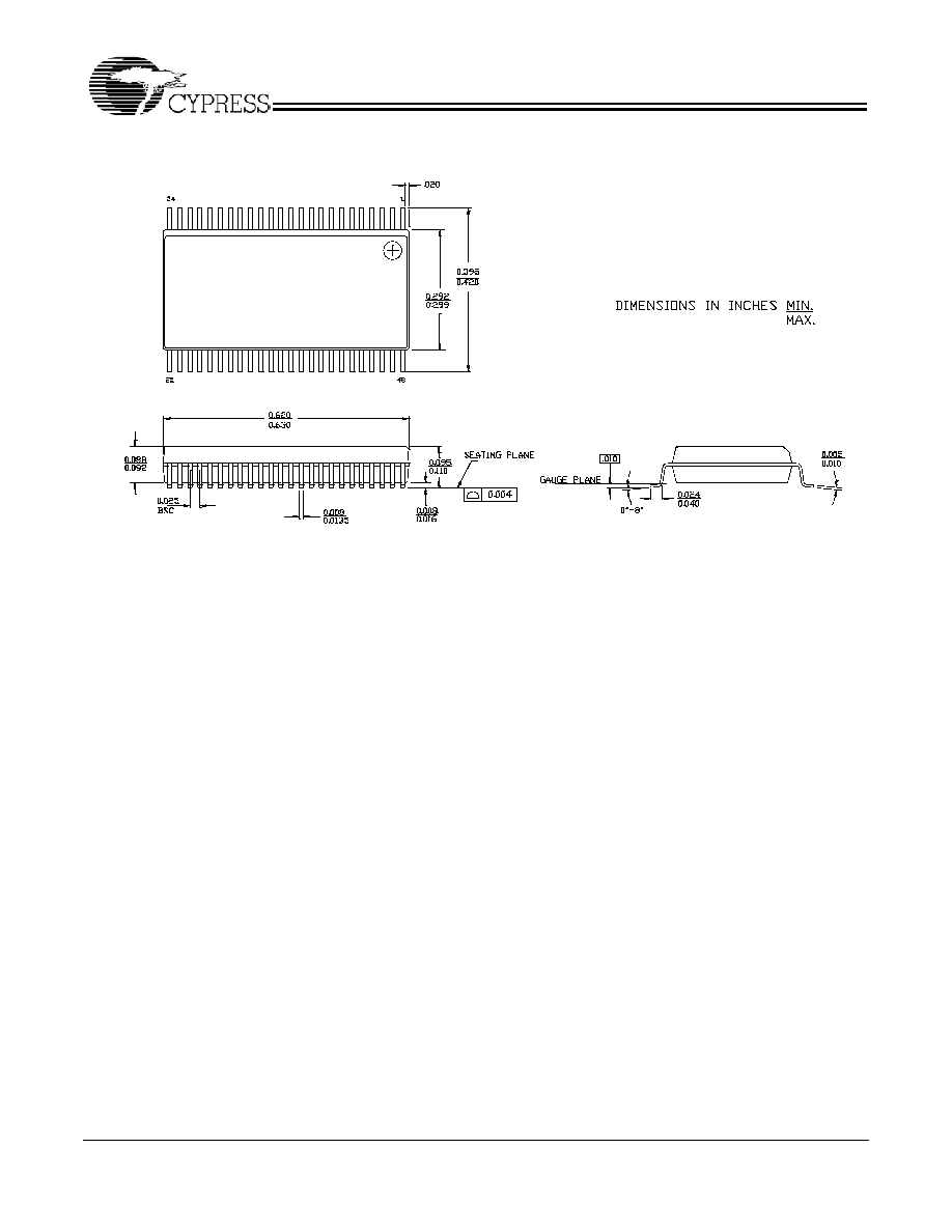
Package Drawing and Dimensions
Purchase of I
2
C components from Cypress, or one of its sublicensed Associated Companies, conveys a license under the Philips
I
2
C Patent Rights to use these components in an I
2
C system, provided that the system conforms to the I
2
C Standard Specification
as defined by Philips. Intel and Pentium are registered trademarks of Intel Corporation. Dial-A-Frequency is a registered trademark
of Cypress Semiconductor. All product and company names mentioned in this document are the trademarks of their respective
holders.
48-lead Shrunk Small Outline Package O48
51-85061-*C
CY28404
Document #: 38-07510 Rev. *B
Page 20 of 20
Document History Page
Document Title: CY28404 CK409-Compliant Clock Synthesizer
Document Number: 38-07510
REV.
ECN NO.
Issue
Date
Orig. of
Change
Description of Change
**
125355
04/14/03
RGL
New Data Sheet
*A
127160
06/16/03
RGL
Removed the SRC functionality
Modified the title to CK409-Compliant Clock Synthesizer
*B
235908
See ECN
RGL
Removed all items referencing to 166MHz
Added Lead Free devices