 | –≠–ª–µ–∫—Ç—Ä–æ–Ω–Ω—ã–π –∫–æ–º–ø–æ–Ω–µ–Ω—Ç: CY28409 | –°–∫–∞—á–∞—Ç—å:  PDF PDF  ZIP ZIP |
Clock Synthesizer with Differential SRC and CPU Outputs
CY28409
Cypress Semiconductor Corporation
∑
3901 North First Street
∑
San Jose
,
CA 95134
∑
408-943-2600
Document #: 38-07445 Rev. *B
Revised August 26, 2003
Features
∑ Supports Intel
Pentium
4-type CPUs
∑ Selectable CPU frequencies
∑ 3.3V power supply
∑ Ten copies of PCI clocks
∑ Five copies of 3V66 with one optional VCH
∑ Two copies 48-MHz USB clocks
∑ Three differential CPU clock pairs
∑ One differential SRC clock
∑ I
2
C support with readback capabilities
∑ Ideal Lexmark Spread Spectrum profile for maximum
EMI reduction
∑ 56-pin SSOP and TSSOP packages
Note:
1.
Signals marked with [*] and [**] have internal pull-up and pull-down resistors, respectively.
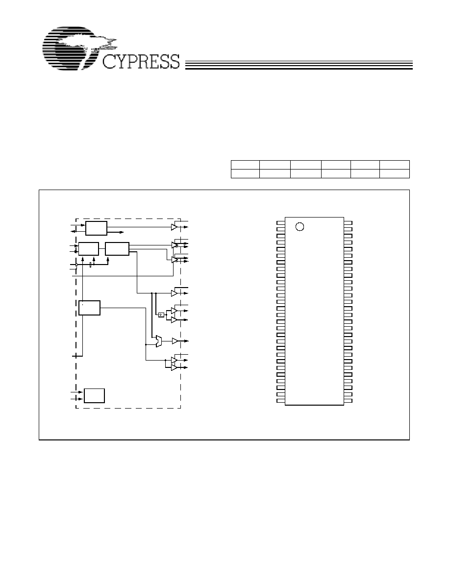
CPU
SRC
3V66
PCI
REF
48M
x 3
x 1
x 5
x 10
x 2
x 2
Block Diagram
Pin Configuration
REF_0
REF_1
XIN
XOUT
VSS_REF
PCIF0
PCIF1
PCIF2
VDD_PCI
VSS_PCI
PCI0
PCI1
PCI2
PCI3
VDD_PCI
VSS_PCI
PCI4
PCI5
PCI6
PD#
3V66_0
3V66_1
VDD_3V66
VSS_3V66
FS_B
VDD_A
SDATA
VDD_SRC
SRCT
SRCC
VSS_SRC
CPUT0
CPUC0
VDD_CPU
CPUT1
CPUC1
VSS_CPU
CPUT2
CPUC2
VDD_CPU
CPU_STP#
FS_A
VSS_IREF
IREF
VSS_A
VTT_PWRGD#
3V66_2
3V66_3
SCLK
VDD_48
VSS_48
USB_48
3V66_4/VCH
56
55
54
53
52
51
50
49
48
47
46
45
44
43
42
41
40
39
38
37
36
35
34
33
1
2
3
4
5
6
7
8
9
10
11
12
13
14
15
16
17
18
19
20
21
22
23
24
25
26
27
28
32
31
30
29
~
VDD_REF
XTAL
PLL Ref Freq
XOUT
XIN
VDD_PCI
OSC
SCLK
PLL1
I
2
C
Logic
VDD_48MHz
SDATA
VDD_3V66
Divider
Network
VDD_CPU
FS_[A:B]
PD#
REF0:1
VTT_PWRGD#
IREF
3V66_[0:3]
PCIF[0:2]
PCI[0:6]
DOT_48
3V66_4/VCH
2
PLL2
CPUT[0:2], CPUC[0:2]
VDD_SRC
SRCT, SRCC
USB_48
CPU_STP#
PCI_STP#
VDD_REF
DOT_48
PCI_STP#
C
Y
28
409
56 SSOP/TSSOP
[1]
CY28409
Document #: 38-07445 Rev. *B
Page 2 of 18
Pin Description
Pin No.
Name
Type
Description
1, 2
REF(0:1)
O, SE Reference Clock. 3.3V 14.318-Mz clock output.
4
XIN
I
Crystal Connection or External Reference Frequency Input. This pin has dual
functions. It can be used as an external 14.318-MHz crystal connection or as an external
reference frequency input.
5
XOUT
O, SE Crystal Connection. Connection for an external 14.318-MHz crystal output.
41,44,47
CPUT(0:2)
O, DIF CPU Clock Output. Differential CPU clock outputs. See Table 1 for frequency config-
uration
40,43,46
CPUC(0:2)
O, DIF CPU Clock Output. Differential CPU clock outputs. See Table 1 for frequency config-
uration
38, 37
SRCT, SRCC
O, DIF Differential serial reference clock.
22,23,26,27
3V66(0:3)
O, SE 66-MHz Clock Output. 3.3V 66-MHz clock from internal VCO.
29
3V66_4VCH
O, SE 48-/66-MHz Clock Output. 3.3V selectable through SMBus to be 66 or 48 MHz.
7,8,9
PCIF(0:2)
O, SE Free-running PCI Output. 33-MHz clocks divided down from 3V66.
12,13,14,
15,18,19,20
PCI(0:6)
O, SE PCI Clock Output. 33-MHz clocks divided down from 3V66.
31,
USB_48
O, SE Fixed 48-MHz clock output.
32
DOT_48
O, SE Fixed 48-MHz clock output.
51,56
FS_A, FS_B
I
3.3V LVTTL input for CPU frequency selection.
52
IREF
I
Current Reference. A precision resistor is attached to this pin which is connected to
the internal current reference.
21
PD#
I, PU
3.3V LVTTL input for PowerDown# active low.
50
CPU_STP#
I, PU
3.3V LVTTL input for CPU_STP# active low.
49
PCI_STP#
I, PU
3.3V LVTTL input for PCI_STP# active low.
35
VTT_PWRGD#
I
3.3V LVTTL input is a level sensitive strobe used to latch the FS_A and FS_B
inputs (active low).
30
SDATA
I/O
SMBus-compatible SDATA.
28
SCLK
I
SMBus-compatible SCLOCK.
53
VSS_IREF
GND
Ground for current reference.
55
VDD_A
PWR
3.3V power supply for PLL.
54
VSS_A
GND
Ground for PLL.
42,48
VDD_CPU
PWR
3.3V power supply for outputs.
45
VSS_CPU
GND
Ground for outputs.
36
VDD_SRC
PWR
3.3V power supply for outputs.
39
VSS_SRC
GND
Ground for outputs.
34
VDD_48
PWR
3.3V power supply for outputs.
33
VSS_48
GND
Ground for outputs.
10,16
VDD_PCI
PWR
3.3V power supply for outputs.
11,17
VSS_PCI
GND
Ground for outputs.
24
VDD_3V66
PWR
3.3V power supply for outputs.
25
VSS_3V66
GND
Ground for outputs.
3
VDD_REF
PWR
3.3V power supply for outputs.
6
VSS_REF
GND
Ground for outputs.
CY28409
Document #: 38-07445 Rev. *B
Page 3 of 18
Frequency Select Pins (FS_A, FS_B)
Host clock frequency selection is achieved by applying the
appropriate logic levels to FS_A and FS_B inputs prior to
VTT_PWRGD# assertion (as seen by the clock synthesizer).
Upon VTT_PWRGD# being sampled low by the clock chip
(indicating processor VTT voltage is stable), the clock chip
samples the FS_A and FS_B input values. For all logic levels
of FS_A and FS_B except MID, VTT_PWRGD# employs a
one-shot functionality in that once a valid low on
VTT_PWRGD# has been sampled low, all further
VTT_PWRGD#, FS_A and FS_B transitions will be ignored. In
the case where FS_B is at mid level when VTT_PWRGD# is
sampled low, the clock chip will assume "Test Clock Mode".
Once "Test Clock Mode" has been invoked, all further FS_B
transitions will be ignored and FS_A will asynchronously
select between the Hi-Z and REF/N mode. Exiting test mode
is accomplished by cycling power with FS_B in a high or low
state.
Serial Data Interface
To enhance the flexibility and function of the clock synthesizer,
a two-signal serial interface is provided. Through the Serial
Data Interface, various device functions, such as individual
clock output buffers, can be individually enabled or disabled.
The registers associated with the Serial Data Interface
initializes to their default setting upon power-up, and therefore
use of this interface is optional. Clock device register changes
are normally made upon system initialization, if any are
required. The interface cannot be used during system
operation for power management functions.
Data Protocol
The clock driver serial protocol accepts byte write, byte read,
block write, and block read operations from the controller. For
block write/read operation, the bytes must be accessed in
sequential order from lowest to highest byte (most significant
bit first) with the ability to stop after any complete byte has
been transferred. For byte write and byte read operations, the
system controller can access individually indexed bytes. The
offset of the indexed byte is encoded in the command code,
as described in Table 3.
The block write and block read protocol is outlined in Table 4
while Table 5 outlines the corresponding byte write and byte
read protocol. The slave receiver address is 11010010 (D2h).
Table 1. Frequency Select Table (FS_A FS_B)
FS_A
FS_B
CPU
SRC
3V66
PCIF/PCI
REF0
REF1
USB/DOT
0
0
100 MHz
100/200 MHz
66 MHz
33 MHz
14.3 MHz
14.31 MHz
48 MHz
0
MID
REF/N
REF/N
REF/N
REF/N
REF/N
REF/N
REF/N
0
1
200 MHz
100/200 MHz
66 MHz
33 MHz
14.3 MHz
14.31 MHz
48 MHz
1
0
133 MHz
100/200 MHz
66 MHz
33 MHz
14.3 MHz
14.31 MHz
48 MHz
1
MID
Hi-Z
Hi-Z
Hi-Z
Hi-Z
Hi-Z
Hi-Z
Hi-Z
Table 2. Frequency Select Table (FS_A FS_B) SMBus Bit 5 of Byte 6 = 1
FS_A
FS_B
CPU
SRC
3V66
PCIF/PCI
REF0
REF1
USB/DOT
0
0
200 MHz
100/200 MHz
66 MHz
33 MHz
14.3 MHz
14.31 MHz
48 MHz
0
1
400 MHz
100/200 MHz
66 MHz
33 MHz
14.3 MHz
14.31 MHz
48 MHz
1
0
266 MHz
100/200 MHz
66 MHz
33 MHz
14.3 MHz
14.31 MHz
48 MHz
Table 3. Command Code Definition
Bit
Description
7
0 = Block read or block write operation, 1 = Byte read or byte write operation
(6:0)
Byte offset for byte read or byte write operation. For block read or block write operations, these bits should be
'0000000'
Table 4. Block Read and Block Write Protocol
Block Write Protocol
Block Read Protocol
Bit
Description
Bit
Description
1
Start
1
Start
2:8
Slave address ≠ 7 bits
2:8
Slave address ≠ 7 bits
9
Write = 0
9
Write = 0
10
Acknowledge from slave
10
Acknowledge from slave
11:18
Command Code ≠ 8 Bit
'00000000' stands for block operation
11:18
Command Code ≠ 8 Bit
'00000000' stands for block operation
19
Acknowledge from slave
19
Acknowledge from slave
CY28409
Document #: 38-07445 Rev. *B
Page 4 of 18
Control Registers
20:27
Byte Count ≠ 8 bits
20
Repeat start
28
Acknowledge from slave
21:27
Slave address ≠ 7 bits
29:36
Data byte 1 ≠ 8 bits
28
Read = 1
37
Acknowledge from slave
29
Acknowledge from slave
38:45
Data byte 2 ≠ 8 bits
30:37
Byte count from slave ≠ 8 bits
46
Acknowledge from slave
38
Acknowledge from master
....
......................
39:46
Data byte from slave ≠ 8 bits
....
Data Byte (N≠1) ≠8 bits
47
Acknowledge from master
....
Acknowledge from slave
48:55
Data byte from slave ≠ 8 bits
....
Data Byte N ≠8 bits
56
Acknowledge from master
....
Acknowledge from slave
....
Data byte N from slave ≠ 8 bits
....
Stop
....
Acknowledge from master
....
Stop
Table 4. Block Read and Block Write Protocol(continued)
Block Write Protocol
Block Read Protocol
Bit
Description
Bit
Description
Table 5. Byte Read and Byte Write protocol
Byte Write Protocol
Byte Read Protocol
Bit
Description
Bit
Description
1
Start
1
Start
2:8
Slave address ≠ 7 bits
2:8
Slave address ≠ 7 bits
9
Write = 0
9
Write = 0
10
Acknowledge from slave
10
Acknowledge from slave
11:18
Command Code ≠ 8 bits
'100xxxxx' stands for byte operation, bits[4:0] of the
command code represents the offset of the byte to
be accessed
11:18
Command Code ≠ 8 bits
'100xxxxx' stands for byte operation, bits[4:0] of
the command code represents the offset of the
byte to be accessed
19
Acknowledge from slave
19
Acknowledge from slave
20:27
Data byte from master ≠ 8 bits
20
Repeat start
28
Acknowledge from slave
21:27
Slave address ≠ 7 bits
29
Stop
28
Read = 1
29
Acknowledge from slave
30:37
Data byte from slave ≠ 8 bits
38
Acknowledge from master
39
Stop
Byte 0:Control Register 0
Bit
@Pup
Name
Description
7
0
Reserved
Reserved, Set = 0
6
1
PCIF
PCI
PCI Drive Strength Override
0 = Force All PCI and PCIF Outputs to Low Drive Strength
1 = Force All PCI and PCIF Outputs to High Drive Strength
5
0
Reserved
Reserved, Set = 0
4
0
Reserved
Reserved, Set = 0

CY28409
Document #: 38-07445 Rev. *B
Page 5 of 18
3
Externally
Selected
PCI_STP#
PCI_STP# reflects the current value of the external PCI_STP# pin.
0 =PCI_STP# pin is low.
2
Externally
Selected
CPU_STP#
CPU_STP# reflects the current value of the external CPU_STP# pin.
0 = CPU_STP# pin is low.
1
Externally
Selected
FS_B
FS_B reflects the value of the FS_B pin sampled on power-up.
0
Externally
Selected
FS_A
FS_A reflects the value of the FS_A pin sampled on power-up.
Byte 1: Control Register 1
Bit
@Pup
Name
Description
7
0
SRCT, SRCC
Allows control of SRCT/C with assertion of PCI_STP# or SW PCI_STP
0 = Free Running, 1 = Stopped with PCI_STP#
6
1
SRCT, SRCC
SRCT/C Output Enable; 0 = Disabled (Hi-z), 1 = Enabled
5
1
Reserved
Reserved, Set = 1
4
1
Reserved
Reserved, Set = 1
3
1
Reserved
Reserved, Set = 1
2
1
CPUT2, CPUC2
CPUT/C2 Output Enable; 0 = Disabled (Hi-z), 1 = Enabled
1
1
CPUT1, CPUC1
CPUT/C1 Output Enable; 0 = Disabled (Hi-z), 1 = Enabled
0
1
CPUT0, CPUC0
CPUT/C0 Output Enable; 0 = Disabled (Hi-z), 1 = Enabled
Byte 2: Control Register 2
Bit
@Pup
Name
Description
7
0
SRCT, SRCC
SRCT/C Pwrdwn Drive Mode
0 = Driven during power-down, 1 = Three-state during power-down
6
0
SRCT, SRCC
SRCT/C Stop Drive Mode
0 = Driven during PCI_STP, 1 = Three-state during PCI_STP
5
0
CPUT2, CPUC2
CPUT/C2 Pwrdwn Drive Mode
0 = Driven during power-down, 1 = Three-state during power-down
4
0
CPUT1, CPUC1
CPUT/C1 Pwrdwn Drive Mode
0 = Driven during power `down, 1 = Three-state during power-down
3
0
CPUT0, CPUC0
CPUT/C0 Pwrdwn Drive Mode
0 = Driven during power-down, 1 = Three-state during power-down
2
0
CPUT2, CPUC2
CPUT/C2 stop Drive Mode
0 = Driven when stopped, 1 = Three-state when stopped
1
0
CPUT1, CPUC1
CPUT/C1 stop Drive Mode
0 = Driven when stopped, 1 = Three-state when stopped
0
0
CPUT0, CPUC0
CPUT/C0 stop Drive Mode
0 = Driven when stopped, 1 = Three-state when stopped
Byte 3: Control Register 3
Bit
@Pup
Name
Description
7
1
SW PCI STOP
SW PCI_STP Function
0= PCI_STP assert, 1= PCI_STP deassert
When this bit is set to 0, all STOPPABLE PCI, PCIF and SRC outputs will
be stopped in a synchronous manner with no short pulses.
When this bit is set to 1, all STOPPED PCI,PCIF and SRC outputs will
resume in a synchronous manner with no short pulses.
6
1
PCI6
PCI6 Output Enable
0 = Disabled, 1 = Enabled
Byte 0:Control Register 0 (continued)
Bit
@Pup
Name
Description