Äîêóìåíòàöèÿ è îïèñàíèÿ www.docs.chipfind.ru
PRELIMINARY
Next Generation FTG for Intel® Architecture
CY28416
Cypress Semiconductor Corporation
·
3901 North First Street
·
San Jose
,
CA 95134
·
408-943-2600
Document #: 38-07657 Rev. *A
Revised February 2, 2005
Features
· Supports Intel Pentium
®
4-Type CPUs
· Selectable CPU Frequencies
· Two Differential CPU Clock Pairs
· Four 100-MHz Differential SRC Clock Pairs
· One CPU/SRC Selectable Differential Clock Pair
· One 96-MHz Differential Dot Clock Support
· Two 48-MHz Clocks
· Four 33-MHz PCI Clocks
· Two 33-MHz PCI Free Running Clocks
· Low Voltage Frequency Select Input
· I
2
C Support Byte/Word/Block Read/Write Capabilities
· Ideal Lexmark Spread Spectrum Profile for Maximum
EMI Reduction
· 3.3V Power Supply
· 48-pin SSOP Package
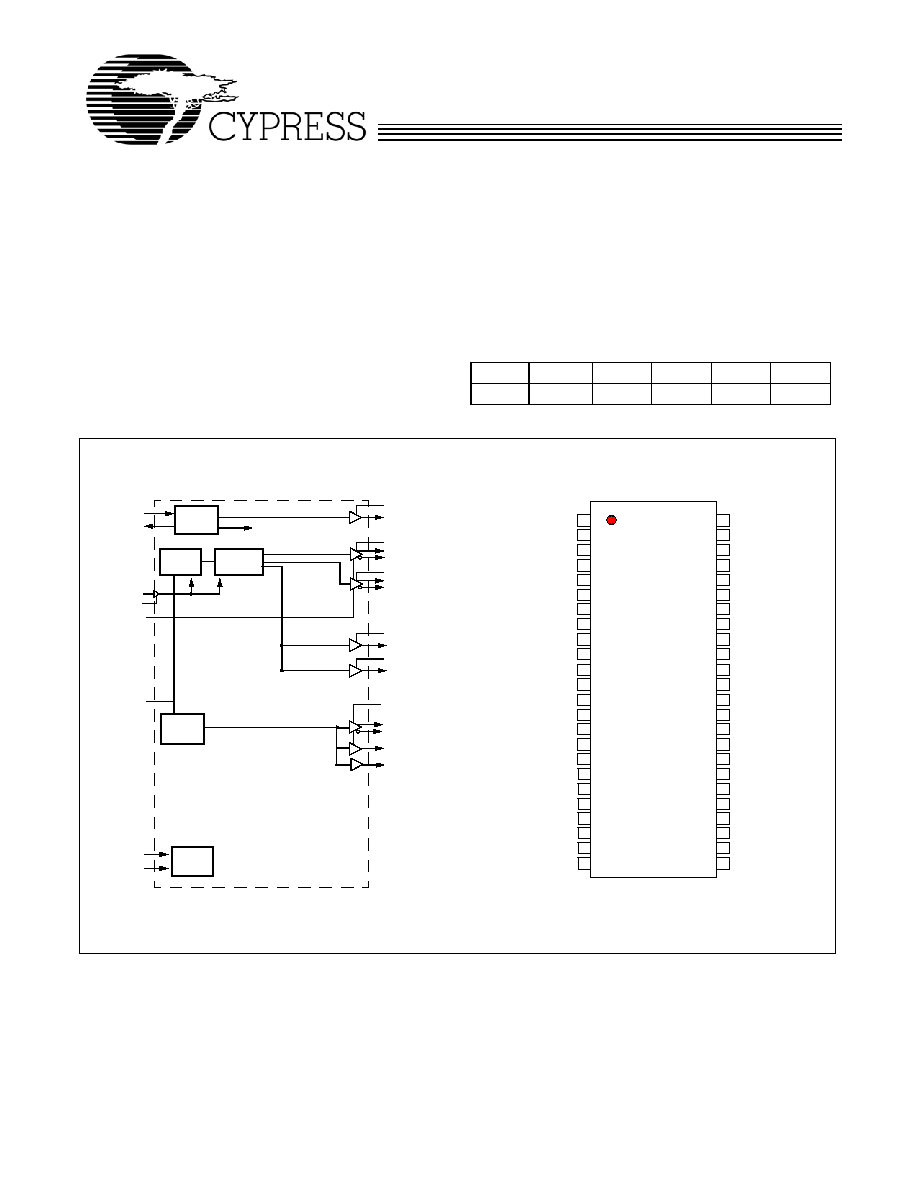
CPU
SRC
PCI
DOT
USB
REF
x2 / x3
x4 / x5
x 6
x 1
x 2
x 2
Block Diagram
Pin Configuration
VDD_REF
XTAL
PLL Ref Freq
XOUT
XIN
OSC
SCLK
PLL1
I
2
C
Logic
VDD_48MHz
SDATA
VDD_PCI
Divider
Network
VDD_CPU
FS_[C:A]
REF
VTT_PWRGD#
IREF
PCI[0:3]
PLL2
CPUT[0:1], CPUC[0:1],
VDD_SRC
SRCT[0:3], SRCC[0:3]
48MHz0
48-PIN SSOP
DOT96T
DOT96C
VDD_PCIF
PCIF[0:1]
PD
CY28416
8
9
10
11
12
13
14
15
16
17
18
19
20
21
22
23
24
1
2
3
4
5
6
7
48
47
46
45
44
43
42
41
40
39
38
37
36
35
34
33
32
31
30
29
SDATA
SCLK
XOUT
XIN
VSS_REF
REF1/FS_A
REF0/FS_C
PCI0
VDD_REF
VDD_PCI
VSS_PCI
PCI2
PCI3
VSS_PCI
VDD_PCI
PCIF0/TESTSEL
PCIF1/ITPEN
VDD_48
48MHz0/FS_B
48MHz1
VSS_48
DOT96T
DOT96C
PCI1
CPUT0
VSS_CPU
CPUC0
VDD_CPU
CPUT1
CPUC1
IREF
VDDA
VSSA
CPUC2_ITP/SRCC4
VDD_SRC
VSS_SRC
SRCT3
SRCC3
VDD_SRC
SRCC2_SATA
SRCT2_SATA
SRCC1
SRCT1
VSS_SRC
SRCC0
SRCT0
VTT_PWRGD#/PD
CPUT2_ITP/SRCT4
28
27
26
25
CPU2/SRC4
48MHz1

PRELIMINARY
CY28416
Document #: 38-07657 Rev. *A
Page 2 of 15
Pin Definition
Pin No.
Name
Type
Description
47,46,44,43
CPUT/C[0:1]
O, DIF Differential CPU clock output.
39,38
CPUT2_ITP/SRCT4
CPUC2_ITP/SRCC4
O, DIF Selectable Differential CPU or SRC clock output.
ITP_EN = 0 @VTT_PWRGD# assertion PIN 39,38 = SRCT4,SRCC4
ITP_EN = 1 @VTT_PWRGD# assertion PIN 39,38 = CPUT2_ITP,CPUC2_ITP
23,24
DOT96T, DOT96C
O, DIF Differential 96-MHz clock output
6
FS_A/REF1
I/O, SE 3.3V tolerant input for CPU frequency/REF clock
Refer to DC Electrical Specifications table for Vil_FS and Vih_FS specifications
.
20
FS_B/48 MHz0
I/O, SE 3.3V tolerant input for CPU frequency/48 MHz clock
Refer to DC Electrical Specifications table for Vil_FS and Vih_FS specifications
.
7
FS_C/REF0
I
/
O, SE 3.3V tolerant input for CPU frequency/REF clock
Refer to DC Electrical Specifications table for Vil_FS and Vih_FS specifications
.
42
IREF
I
A precision resistor is attached to this pin, which is connected to the internal
current reference.
18
ITP_EN/PCIF1
I/O, SE Enable SRC4 or CPU2_ITP/PCIF clock.
(sampled on the VTT_PWRGD# assertion). 0 = SRC4, 1 = CPU2_ITP
9,10,13,14
PCI
O, SE 33-MHz clock output.
21
48 MHz1
O, SE 48-MHz clock output.(Uses same control SMBus register as 48 MHz0 to control
enable/disable.)
1
SCLK
I
SMBus compatible SCLOCK.
2
SDATA
I/O
SMBus compatible SDATA.
26,27,29,30,
34,35
SRCT/C[0:3]
O, DIF Differential Serial reference clock.
31,32
SRCT2_SATA,
SRCC2_SATA
O, DIF Differential Serial reference clock. Recommended output for SATA
17
TEST_SEL/PCIF0
I/O, SE,
PD
LVTTL input for selecting HI-Z or Normal operation/33 MHz Clock
0 = Normal operation, 1 = HI-Z when VTT_PWRGD# is sampled
19
VDD_48
PWR 3.3V power supply for outputs
45
VDD_CPU
PWR 3.3V power supply for outputs
11, 16
VDD_PCI
PWR 3.3V power supply for outputs
8
VDD_REF
PWR 3.3V power supply for outputs
33, 37
VDD_SRC
PWR 3.3V power supply for outputs
40
VDDA
PWR 3.3V power supply for PLL
22
VSS_48
GND Ground for outputs
48
VSS_CPU
GND Ground for outputs
12, 15
VSS_PCI
GND Ground for outputs
5
VSS_REF
GND Ground for outputs
28, 36
VSS_SRC
GND Ground for outputs
41
VSSA
GND Ground for PLL
25
VTT_PWRGD#/PD
I, PD 3.3V LVTTL Input. This pin is a level-sensitive strobe used to latch the FS_A,
FS_B, FS_C/TEST_SEL, and PCIF0/ITP_EN Inputs. After asserting
VTT_PWRGD# (active LOW), this pin becomes a realtime input for asserting
power-down (active HIGH)
4
XIN
I
14.318-MHz Crystal Input
3
XOUT
O
14.318-MHz Crystal Output
PRELIMINARY
CY28416
Document #: 38-07657 Rev. *A
Page 3 of 15
Frequency Select Pins (FS_A, FS_B, and FS_C)
Host clock frequency selection is achieved by applying the
appropriate logic levels to FS_A, FS_B, FS_C inputs prior to
VTT_PWRGD# assertion (as seen by the clock synthesizer).
Upon VTT_PWRGD# being sampled LOW by the clock chip
(indicating processor VTT voltage is stable), the clock chip
samples the FS_A, FS_B, and FS_C input values. For all logic
levels of FS_A, FS_B, and FS_C VTT_PWRGD# employs a
one-shot functionality in that once a valid LOW on
VTT_PWRGD# has been sampled, all further VTT_PWRGD#,
FS_A, FS_B, and FS_C transitions will be ignored, except in
test mode.
Serial Data Interface
To enhance the flexibility and function of the clock synthesizer,
a two-signal serial interface is provided. Through the Serial
Data Interface, various device functions, such as individual
clock output buffers, can be individually enabled or disabled.
The registers associated with the Serial Data Interface initial-
izes to their default setting upon power-up, and therefore use
of this interface is optional. Clock device register changes are
normally made upon system initialization, if any are required.
The interface cannot be used during system operation for pow-
er management functions.
Data Protocol
The clock driver serial protocol accepts byte write, byte read,
block write, and block read operations from the controller. For
block write/read operation, the bytes must be accessed in se-
quential order from lowest to highest byte (most significant bit
first) with the ability to stop after any complete byte has been
transferred. For byte write and byte read operations, the sys-
tem controller can access individually indexed bytes. The off-
set of the indexed byte is encoded in the command code, as
described in Table 2.
The block write and block read protocol is outlined in Table 3
while Table 4 outlines the corresponding byte write and byte
read protocol. The slave receiver address is 11010010 (D2h).
T
Table 1. Frequency Select Table (FS_A FS_B)
FS_C
FS_B
FS_A
CPU
SRC
PCIF/PCI
REF0
DOT96
USB
1
0
1
100 MHz
100 MHz
33 MHz
14.318 MHz
96 MHz
48 MHz
0
0
1
133 MHz
100 MHz
33 MHz
14.318 MHz
96 MHz
48 MHz
0
1
1
166 MHz
100 MHz
33 MHz
14.318 MHz
96 MHz
48 MHz
0
1
0
200 MHz
100 MHz
33 MHz
14.318 MHz
96 MHz
48 MHz
0
0
0
266 MHz
100 MHz
33 MHz
14.318 MHz
96 MHz
48 MHz
1
0
0
333 MHz
100 MHz
33 MHz
14.318 MHz
96 MHz
48 MHz
1
1
0
400 MHz
100 MHz
33 MHz
14.318 MHz
96 MHz
48 MHz
1
1
1
Reserved
100 MHz
33 MHz
14.318 MHz
96 MHz
48 MHz
Table 2. Command Code Definition
Bit
Description
7
0 = Block read or block write operation, 1 = Byte read or byte write operation
(6:0)
Byte offset for byte read or byte write operation. For block read or block write operations, these bits should be '0000000'
Table 3. Block Read and Block Write Protocol
Block Write Protocol
Block Read Protocol
Bit
Description
Bit
Description
1
Start
1
Start
8:2
Slave address 7 bits
8:2
Slave address 7 bits
9
Write 9
Write
10
Acknowledge from slave
10
Acknowledge from slave
18:11
Command Code 8 Bits
18:11
Command Code 8 Bits
19
Acknowledge from slave
19
Acknowledge from slave
27:20
Byte Count 8 bits
(Skip this step if I
2
C_EN bit set)
20
Repeat start
28
Acknowledge from slave
27:21
Slave address 7 bits
36:29
Data byte 1 8 bits
28
Read = 1
37
Acknowledge from slave
29
Acknowledge from slave
45:38
Data byte 2 8 bits
37:30
Byte Count from slave 8 bits
46
Acknowledge from slave
38
Acknowledge
PRELIMINARY
CY28416
Document #: 38-07657 Rev. *A
Page 4 of 15
Control Registers
....
Data Byte /Slave Acknowledges
46:39
Data byte 1 from slave 8 bits
....
Data Byte N 8 bits
47
Acknowledge
....
Acknowledge from slave
55:48
Data byte 2 from slave 8 bits
....
Stop
56
Acknowledge
....
Data bytes from slave / Acknowledge
....
Data Byte N from slave 8 bits
....
NOT Acknowledge
...
Stop
Table 3. Block Read and Block Write Protocol (continued)
Block Write Protocol
Block Read Protocol
Bit
Description
Bit
Description
Table 4. Byte Read and Byte Write protocol
Byte Write Protocol
Byte Read Protocol
Bit
Description
Bit
Description
1
Start
1
Start
8:2
Slave address 7 bits
8:2
Slave address 7 bits
9
Write
9
Write
10
Acknowledge from slave
10
Acknowledge from slave
18:11
Command Code 8 bits
18:11
Command Code 8 bits
19
Acknowledge from slave
19
Acknowledge from slave
27:20
Data byte 8 bits
20
Repeated start
28
Acknowledge from slave
27:21
Slave address 7 bits
29
Stop
28
Read
29
Acknowledge from slave
37:30
Data from slave 8 bits
38
NOT Acknowledge
39
Stop
Byte 0:Control Register 0
Bit
@Pup
Name
Description
7
1
CPUT2_ITP/SRCT4
CPUC2_ITP/SRCC4
CPU[T/C]2_ITP/SRC[T/C]4 Output Enable
0 = Disable (Hi-Z), 1 = Enable
6
1
RESERVED
RESERVED, Set = 1
5
1
RESERVED
RESERVED, Set = 1
4
1
SRC[T/C]3
SRC[T/C]3 Output Enable
0 = Disable (Hi-Z), 1 = Enable
3
1
SRC[T/C]2_SATA
SRC[T/C]2_SATA Output Enable
0 = Disable (Hi-Z), 1 = Enable
2
1
SRC[T/C]1
SRC[T/C]1 Output Enable
0 = Disable (Hi-Z), 1 = Enable
1
1
SRC[T/C]0
SRC[T/C]0 Output Enable
0 = Disable (Hi-Z), 1 = Enable
0
1
RESERVED
RESERVED, Set = 1
PRELIMINARY
CY28416
Document #: 38-07657 Rev. *A
Page 5 of 15
Byte 1: Control Register 1
Bit
@Pup
Name
Description
7
1
RESERVED
RESERVED, Set = 1
6
1
DOT_96T/C
DOT_96 MHz Output Enable
0 = Disable (Hi-Z), 1 = Enabled
5
1
48 MHz0, 48 MHz1
48 MHz Output Enable
0 = Disabled, 1 = Enabled
4
1
REF0
REF Output Enable
0 = Disabled, 1 = Enabled
3
1
REF1
REF Output Enable
0 = Disabled, 1 = Enabled
2
1
CPU[T/C]1 CPU[T/C]1 Output Enable
0 = Disable (Hi-Z), 1 = Enabled
1
1
CPU[T/C]0
CPU[T/C]0 Output Enable
0 = Disable (Hi-Z), 1 = Enabled
0
0
CPUT/C
SRCT/C
PCIF
PCI
Spread Spectrum Enable
0 = Spread off, 1 = Spread on
Byte 2: Control Register 2
Bit
@Pup
Name
Description
7
1
PCI3
PCI3 Output Enable
0 = Disabled, 1 = Enabled
6
1
PCI2
PCI2 Output Enable
0 = Disabled, 1 = Enabled
5
1
RESERVED
RESERVED, Set = 1
4
1
RESERVED
RESERVED, Set = 1
3
1
PCI1
PCI1 Output Enable
0 = Disabled, 1 = Enabled
2
1
PCI0
PCI0 Output Enable
0 = Disabled, 1 = Enabled
1
1
PCIF1
PCIF2 Output Enable
0 = Disabled, 1 = Enabled
0
1
PCIF0
PCIF1 Output Enable
0 = Disabled, 1 = Enabled
Byte 3: Control Register 3
Bit
@Pup
Name
Description
7
0
SRC[T/C]4
Allow control of SRC[T/C]4 with assertion of SW PCI_STP#
0 = Free running, 1 = Stopped with PCI_STP#
6
0
RESERVED
RESERVED, Set = 0
5
0
RESERVED
RESERVED, Set = 0
4
0
SRC[T/C]3
Allow control of SRC[T/C]3 with assertion of SW PCI_STP#
0 = Free running, 1 = Stopped with PCI_STP#
3
0
SRC2_SATA
Allow control of SRC2_SATA with assertion of SW PCI_STP#
0 = Free running, 1 = Stopped with PCI_STP#
2
0
SRC[T/C]1
Allow control of SRC[T/C]1 with assertion of SW PCI_STP#
0 = Free running, 1 = Stopped with PCI_STP#
1
0
SRC[T/C]0
Allow control of SRC[T/C]1 with assertion of SW PCI_STP#
0 = Free running, 1 = Stopped with PCI_STP#
0
0
RESERVED
RESERVED, Set = 0