Äîêóìåíòàöèÿ è îïèñàíèÿ www.docs.chipfind.ru
PRELIMINARY
Clock Generator for Intel
Grantsdale Chipset
CY28435
Cypress Semiconductor Corporation
·
3901 North First Street
·
San Jose
,
CA 95134
·
408-943-2600
Document #: 38-07664 Rev. *B
Revised December 21, 2004
Features
· Compliant to Intel
CK410
· Supports Intel Prescott and Tejas CPU
· Selectable CPU frequencies
· Differential CPU clock pairs
· 100-MHz differential SRC clocks
· 96-MHz differential dot clock
· 48-MHz USB clocks
· 33-MHz PCI clock
· Dynamic Frequency Control
· Dial-A-Frequency
· Watchdog
· Two Independent Overclocking PLLs
· Low-voltage frequency select input
· I
2
C support with readback capabilities
· Ideal Lexmark Spread Spectrum profile for maximum
electromagnetic interference (EMI) reduction
· 3.3V power supply
· 56-pin SSOP and TSSOP packages
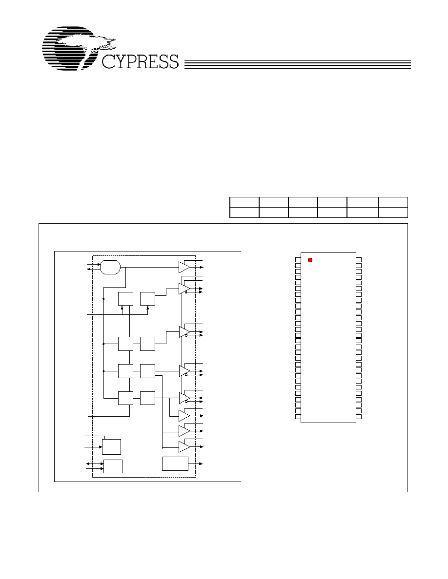
CPU
SRC
PCI
REF
DOT96
USB
x 2
x 7
x 9
x 2
x 1
x 2
Block Diagram
Pin Configuration
VDD_RE
F
VDD_CPU
VDD_SRC
VTTPWR_GD#/PD
PLL Reference
VDD_SRC
VDD_PCI
FS_[E:A]
SRC
PLL
CPU
PLL
VDD_48Mhz
VDD_48
SDATA
PLL
Divider
Divider
FIX
PLL
Divider
Divider
VDD_SRC
VDD_CPU
IREF
RE
F
CPUT
CPUC
SRCT
SRCC
SRCT4_SATA
SRCC4_SATA
DOT96T
DOT96C
USB
PCI
Watchdog
Timer
SRESET#
I2C
Logic
SDATA
SCLK
14.318MHz
Crystal
Xin
Xout
VDD_PCI
PCIF
ITP_EN
Dynamic
Frequency
DF[2:0]
DF_EN
CY28435
8
9
10
11
12
13
14
15
16
17
18
19
20
21
22
23
24
25
26
27
28
1
2
3
4
5
6
7
56
55
54
53
52
51
50
49
48
47
46
45
44
43
42
41
40
39
38
37
36
35
34
33
32
31
30
29
VSS_PCI
VDD_PCI
DF2
/PCI3
*FS_E/PCI4
PCI5
VSS_PCI
VDD_PCI
**SRESET_EN/PCIF1
**DF_EN
/PCIF0
VDD_48
USB48_0
VSS_48
DOT96T
DOT96C
*FS_B/USB48_1
**VTTPWRGD#/PD
**FS_A
SRCT1
SRCC1
VDD_SRC
SRCT2
SRCC2
SRCT3
SRCC3
SRCT4_SATA
SRCC4_SATA
VDD_SRC
PCIF2
PCI1/
DF0
PCI2/
DF1
PCI0/SRESET#
REF1/**FS_C
REF0/**FS_D
VSS_REF
XIN
VDD_REF
XOUT
SCLK
VSS_CPU
CPUT0
CPUC0
VDD_CPU
CPUT1
CPUC1
IREF
VSSA
VDDA
SRCT7
SRCC7
VDD_SRC
SRCT6
SRCC6
SRCT5
SRCC5
VSS_SRC
SDATA
* indicates internal pull-up
** indicates internal pull-down
PRELIMINARY
CY28435
Document #: 38-07664 Rev. *B
Page 2 of 23
Pin Description
Pin No.
Name
Type
Description
1,7
VDD_PCI
PWR 3.3V power supply for outputs.
2,6
VSS_PCI
GND Ground for outputs.
3,55,56
DF/PCI
I/O, SE 3.3V LVTTL input to enable Dynamic Frequency input/33-MHz clock output.
4
FS_E/PCI4
I/O,PU,
SE
3.3V-tolerant input for CPU frequency selection/33-MHz clock.
Refer to DC Electrical Specifications table for Vil_FS and Vih_FS specifications.
5
PCI
O, SE 33-MHz clock.
8
DF_EN/PCIF0
I/O, SE,
PD
3.3V LVTTL input to enable Dynamic Frequency input/33-MHz clock output.
(sampled on the VTT_PWRGD# assertion).
1 = Enable, 0 = Disable
9
SRESET_EN/PCIF
1
I/O, SE,
PD
3.3V LVTTL input to enable Watchdog/33-MHz clocks.
1 = Enable, 0 = Disable
10
PCIF2
O, SE 33-MHz clocks.
17
VTT_PWRGD#/PD
I, PD 3.3V LVTTL input. This pin is a level sensitive strobe used to latch the FS_A,
FS_B, FS_C,FS_D and FS_E inputs. After VTT_PWRGD# (active LOW) assertion,
this pin becomes a real-time input for asserting power down (active HIGH).
11
VDD_48
PWR 3.3V power supply for outputs.
12
USB48_0
O
48-MHz clock output.
18
FS_A
I, PD 3.3V-tolerant input for CPU frequency selection.
Refer to DC Electrical Specifications table for Vil_FS and Vih_FS specifications.
13
VSS_48
GND Ground for outputs.
14,15
DOT96T, DOT96C
O, DIF Fixed 96-MHz clock output.
16
FS_B/USB48_1
I/O, PU,
SE
3.3V-tolerant input for CPU frequency selection/fixed 48-MHz clock output.
Refer to DC Electrical Specifications table for Vil_FS and Vih_FS specifications.
19,20,22,23,
24,25,30,31,
32,33,36, 35
SRCT/C
O, DIF Differential serial reference clocks. Outputs have overclocking capability.
21,28,34
VDD_SRC
PWR 3.3V power supply for outputs.
26,27
SRC4_SATAT,
SRC4_SATAC
O, DIF Differential serial reference clock. Recommended output for SATA.
29
VSS_SRC
GND Ground for outputs.
37
VDDA
PWR 3.3V power supply for PLL.
38
VSSA
GND Ground for PLL.
39
IREF
I
A precision resistor is attached to this pin, which is connected to the internal
current reference.
42
VDD_CPU
PWR 3.3V power supply for outputs.
41,40,44,43 CPUT/C
O, DIF Differential CPU clock outputs.
45
VSS_CPU
GND Ground for outputs.
46
SCLK
I
SMBus-compatible SCLOCK.
47
SDATA
I/O
SMBus-compatible SDATA.
48
VDD_REF
PWR 3.3V power supply for outputs.
49
XOUT
O, SE 14.318-MHz crystal output.
50
XIN
I
14.318-MHz crystal input.
51
VSS_REF
GND Ground for outputs.
52
FS_D/REF0
I/O, SE,
PD
3.3V-tolerant input for CPU frequency selection/Reference clock.
Refer to DC Electrical Specifications table for Vil_FS and Vih_FS specifications.
PRELIMINARY
CY28435
Document #: 38-07664 Rev. *B
Page 3 of 23
Frequency Select Pins (FS_[A:E])
Host clock frequency selection is achieved by applying the
appropriate logic levels to FS_A, FS_B, FS_C,FS_D and
FS_E inputs prior to VTT_PWRGD# assertion (as seen by the
clock synthesizer). Upon VTT_PWRGD# being sampled LOW
by the clock chip (indicating processor VTT voltage is stable),
the clock chip samples the FS_A, FS_B, FS_C,FS_D and
FS_E input values. For all logic levels of FS_A, FS_B,
FS_C,FS_D and FS_E, VTT_PWRGD# employs a one-shot
functionality in that once a valid low on VTT_PWRGD# has
been sampled, all further VTT_PWRGD#, FS_A, FS_B,
FS_C,FS_D and FS_E transitions will be ignored, except in
test mode.
FS_C is a three level input, when sampled at a voltage greater
than 2.1V by VTTPWRGD#, the device will enter test mode as
selected by the voltage level on the FS_B input.
Serial Data Interface
To enhance the flexibility and function of the clock synthesizer,
a two-signal serial interface is provided. Through the Serial
53
FS_C/REF1
I/O,
PD
3.3V-tolerant input for CPU frequency selection/Reference clock.
Selects test mode if pulled to V
IHFS_C
when VTT_PWRGD# is asserted LOW.
Refer to DC Electrical Specifications table for V
ILFS_C
,V
IMFS_C
,V
IHFS_C
specifica-
tions.
54
SRESET#/PCI0
O, PU 3.3V LVTTL output for Watchdog reset/33-MHz clock output.
When configured as SRESET# output this output becomes open drain type with a
high (>100 k
) internal pull-up resistor.
Pin Description
(continued)
Pin No.
Name
Type
Description
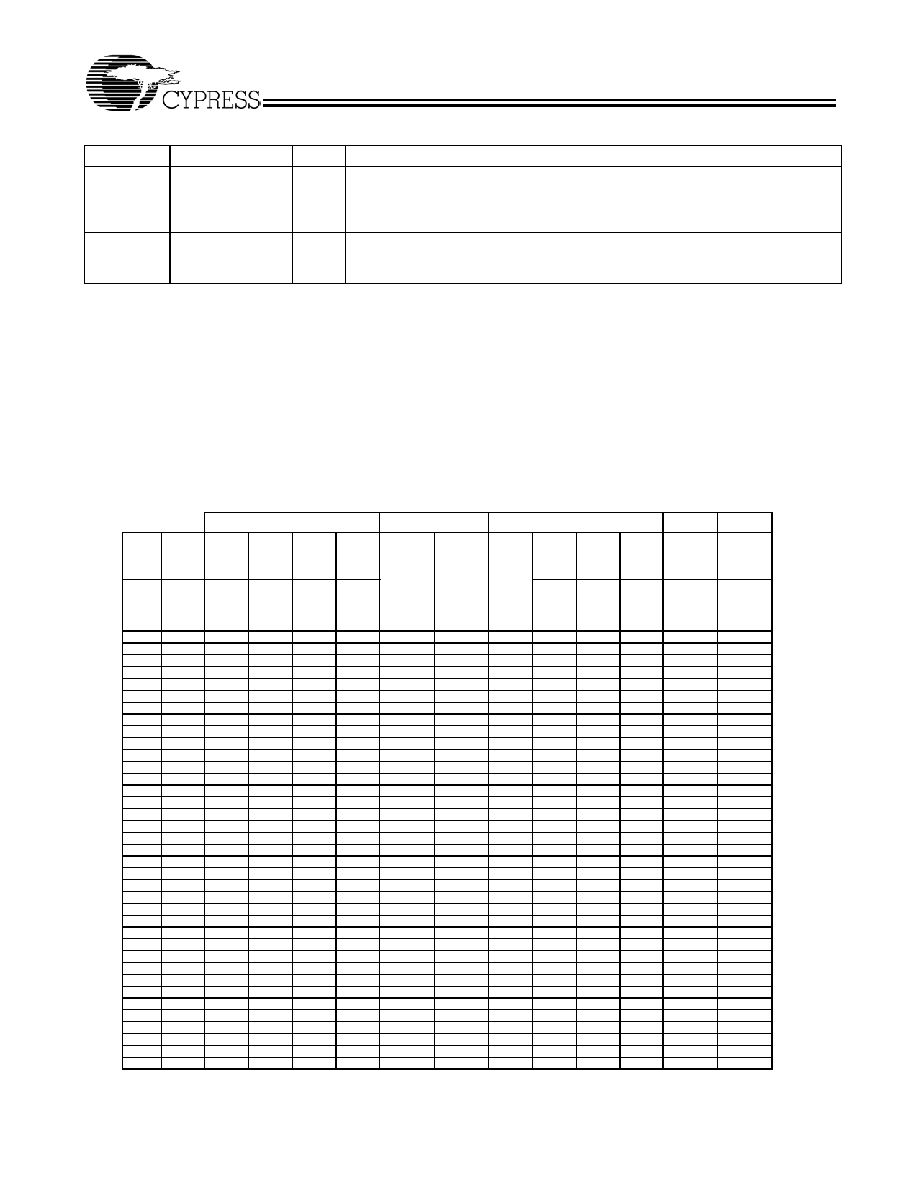
Figure 1. CPU and SRC Frequency Select Tables
No Spread Spectrum and Center spread spectrum on CPU PLL
FS_E
FS_D
FS_C
FS_B
FS_A
CPU
SRC
CPU PLL
Gear
Constant
s
CPU M
divider
CPU N
DEFAULT
CPU N
allowable
range for
DAF
SRC PLL
Gear
Constants
SRC M
divider (not
changeable
by user)
FS_5
(byte 16
bit 5)
HW only FSEL_3
FSEL_2
FSEL_1
FSEL_0
(MHz)
(MHz)
(G)
0
1
0
1
0
1
100
100
30
60
200
200 - 250
30
60
0
1
0
0
0
1
133.3333333
100
40
60
200
200 - 250
30
60
0
1
0
0
1
1
166.6666667
100
60
63
175
175 - 262
30
60
0
1
0
0
1
0
200
100
60
60
200
200 - 250
30
60
0
1
0
0
0
0
266.6666667
100
80
60
200
200 - 250
30
60
0
1
0
1
0
0
333.3333333
100
120
63
175
175 - 262
30
60
0
1
0
1
1
0
400
100
120
60
200
200 - 250
30
60
0
1
1
1
0
1
100.952381
100
30
63
212
212 - 262
30
60
0
1
1
0
0
1
133.968254
100
40
63
211
211 - 262
30
60
0
1
1
0
1
1
167
100
60
60
167
167 - 250
30
60
0
1
1
0
1
0
200.952381
100
60
63
211
211 - 262
30
60
0
1
1
0
0
0
266.6666667
100
80
60
200
200 - 250
30
60
0
1
1
1
0
0
334
100
120
60
167
167 - 250
30
60
0
1
1
1
1
0
400.6451613
100
120
62
207
207 - 258
30
60
0
0
0
1
0
1
100
111.333333
30
60
200
200 - 250
40
60
0
0
0
0
0
1
133.33
111.333333
40
60
200
200 - 250
40
60
0
0
0
0
1
1
166.67
111.333333
60
63
175
175 - 262
40
60
0
0
0
0
1
0
200
111.333333
60
60
200
200 - 250
40
60
0
0
0
0
0
0
266.67
111.333333
80
60
200
200 - 250
40
60
0
0
0
1
0
0
333.33
111.333333
120
63
175
175 - 262
40
60
0
0
0
1
1
0
400
111.333333
120
60
200
200 - 250
40
60
0
0
1
1
0
1
100.95
111.333333
30
63
212
212 - 262
40
60
0
0
1
0
0
1
133.97
111.333333
40
63
211
211 - 262
40
60
0
0
1
0
1
1
166.98
111.333333
60
60
167
167 - 250
40
60
0
0
1
0
1
0
200.95
111.333333
60
63
211
211 - 262
40
60
0
0
1
0
0
0
266.67
111.333333
80
60
200
200 - 250
40
60
0
0
1
1
0
0
333.97
111.333333
120
60
167
167 - 250
40
60
0
0
1
1
1
0
400.65
111.333333
120
62
207
207 - 258
40
60
1
X
0
1
0
1
100
167
30
60
200
200 - 250
60
60
1
X
0
0
0
1
133.33
167
40
60
200
200 - 250
60
60
1
X
0
0
1
1
166.67
167
60
63
175
175 - 262
60
60
1
X
0
0
1
0
200
167
60
60
200
200 - 250
60
60
1
X
0
0
0
0
266.67
167
80
60
200
200 - 250
60
60
1
X
0
1
0
0
333.33
167
120
63
175
175 - 262
60
60
1
X
0
1
1
0
400
167
120
60
200
200 - 250
60
60
1
X
1
1
0
1
100.95
167
30
63
212
212 - 262
60
60
1
X
1
0
0
1
133.97
167
40
63
211
211 - 262
60
60
Input Conditions
Output Frequency
PRELIMINARY
CY28435
Document #: 38-07664 Rev. *B
Page 4 of 23
Data Interface, various device functions, such as individual
clock output buffers, can be individually enabled or disabled.
The registers associated with the Serial Data Interface
initializes to their default setting upon power-up, and therefore
use of this interface is optional. Clock device register changes
are normally made upon system initialization, if any are
required. The interface cannot be used during system
operation for power management functions.
Data Protocol
The clock driver serial protocol accepts byte write, byte read,
block write, and block read operations from the controller. For
block write/read operation, the bytes must be accessed in
sequential order from lowest to highest byte (most significant
bit first) with the ability to stop after any complete byte has
been transferred. For byte write and byte read operations, the
system controller can access individually indexed bytes. The
offset of the indexed byte is encoded in the command code,
as described in Table 1.
The block write and block read protocol is outlined in Table 2
while Table 3 outlines the corresponding byte write and byte
read protocol. The slave receiver address is 11010010 (D2h).
Table 1. Command Code Definition
Bit
Description
7
0 = Block read or block write operation, 1 = Byte read or byte write operation
(6:0)
Byte offset for byte read or byte write operation. For block read or block write operations, these bits should be
'0000000'
Table 2. Block Read and Block Write Protocol
Block Write Protocol
Block Read Protocol
Bit
Description
Bit
Description
1
Start
1
Start
8:2
Slave address 7 bits
8:2
Slave address 7 bits
9
Write 9
Write
10
Acknowledge from slave
10
Acknowledge from slave
18:11
Command Code 8 bits
18:11
Command Code 8 bits
19
Acknowledge from slave
19
Acknowledge from slave
27:20
Byte Count 8 bits
(Skip this step if I
2
C_EN bit set)
20
Repeat start
28
Acknowledge from slave
27:21
Slave address 7 bits
36:29
Data byte 1 8 bits
28
Read = 1
37
Acknowledge from slave
29
Acknowledge from slave
45:38
Data byte 2 8 bits
37:30
Byte Count from slave 8 bits
46
Acknowledge from slave
38
Acknowledge
....
Data Byte /Slave Acknowledges
46:39
Data byte 1 from slave 8 bits
....
Data Byte N 8 bits
47
Acknowledge
....
Acknowledge from slave
55:48
Data byte 2 from slave 8 bits
....
Stop
56
Acknowledge
....
Data bytes from slave / Acknowledge
....
Data Byte N from slave 8 bits
....
NOT Acknowledge
....
Stop
Table 3. Byte Read and Byte Write Protocol
Byte Write Protocol
Byte Read Protocol
Bit
Description
Bit
Description
1
Start
1
Start
8:2
Slave address 7 bits
8:2
Slave address 7 bits
9
Write
9
Write
10
Acknowledge from slave
10
Acknowledge from slave
PRELIMINARY
CY28435
Document #: 38-07664 Rev. *B
Page 5 of 23
Control Registers
18:11
Command Code 8 bits
18:11
Command Code 8 bits
19
Acknowledge from slave
19
Acknowledge from slave
27:20
Data byte 8 bits
20
Repeated start
28
Acknowledge from slave
27:21
Slave address 7 bits
29
Stop
28
Read
29
Acknowledge from slave
37:30
Data from slave 8 bits
38
NOT Acknowledge
39
Stop
Table 3. Byte Read and Byte Write Protocol (continued)
Byte Write Protocol
Byte Read Protocol
Bit
Description
Bit
Description
Byte 0: Control Register 0
Bit
@Pup
Name
Description
7
1
SRC[T/C]7
SRC[T/C]7 Output Enable
0 = Disable (Tri-state), 1 = Enable
6
1
SRC[T/C]6
SRC[T/C]6 Output Enable
0 = Disable (Tri-state), 1 = Enable
5
1
SRC[T/C]5
SRC[T/C]5 Output Enable
0 = Disable (Tri-state), 1 = Enable
4
1
SRC[T/C]4_SATA
SRC[T/C]4_SATA Output Enable
0 = Disable (Tri-state), 1 = Enable
3
1
SRC[T/C]3
SRC[T/C]3 Output Enable
0 = Disable (Tri-state), 1 = Enable
2
1
SRC[T/C]2
SRC[T/C]2 Output Enable
0 = Disable (Tri-state), 1 = Enable
1
1
SRC[T/C]1
SRC[T/C]1 Output Enable
0 = Disable (Tri-state), 1 = Enable
0
1
RESERVED
RESERVED, Set = 1
Byte 1: Control Register 1
Bit
@Pup
Name
Description
7
1
PCIF0
PCIF0 Output Enable
0 = Disabled, 1 = Enabled
6
1
DOT_96T/C
DOT_96 MHz Output Enable
0 = Disable (Tri-state), 1 = Enabled
5
1
USB48_0
USB48_0 MHz Output Enable
0 = Disabled, 1 = Enabled
4
1
REF0 REF0
Output
Enable
0 = Disabled, 1 = Enabled
3
0
RESERVED
RESERVED, Set = 0
2
1
CPU[T/C]1 CPU[T/C]1
Output
Enable
0 = Disable (Tri-state), 1 = Enabled
1
1
CPU[T/C]0
CPU[T/C]0 Output Enable
0 = Disable (Tri-state), 1 = Enabled
0
0
CPU
PLL1 (CPU PLL) Spread Spectrum Enable
0 = Spread off, 1 = Spread on