 | ÐлекÑÑоннÑй компоненÑ: CY2907SI | СкаÑаÑÑ:  PDF PDF  ZIP ZIP |
Äîêóìåíòàöèÿ è îïèñàíèÿ www.docs.chipfind.ru
CY2907
Single-PLL General-Purpose
EPROM Programmable Clock Generator
Cypress Semiconductor Corporation
·
3901 North First Street
·
San Jose
·
CA 95134
·
408-943-2600
Document #: 38-07137 Rev. **
Revised September 26, 2001
CyClocks is a trademark of Cypress Semiconductor Corporation.
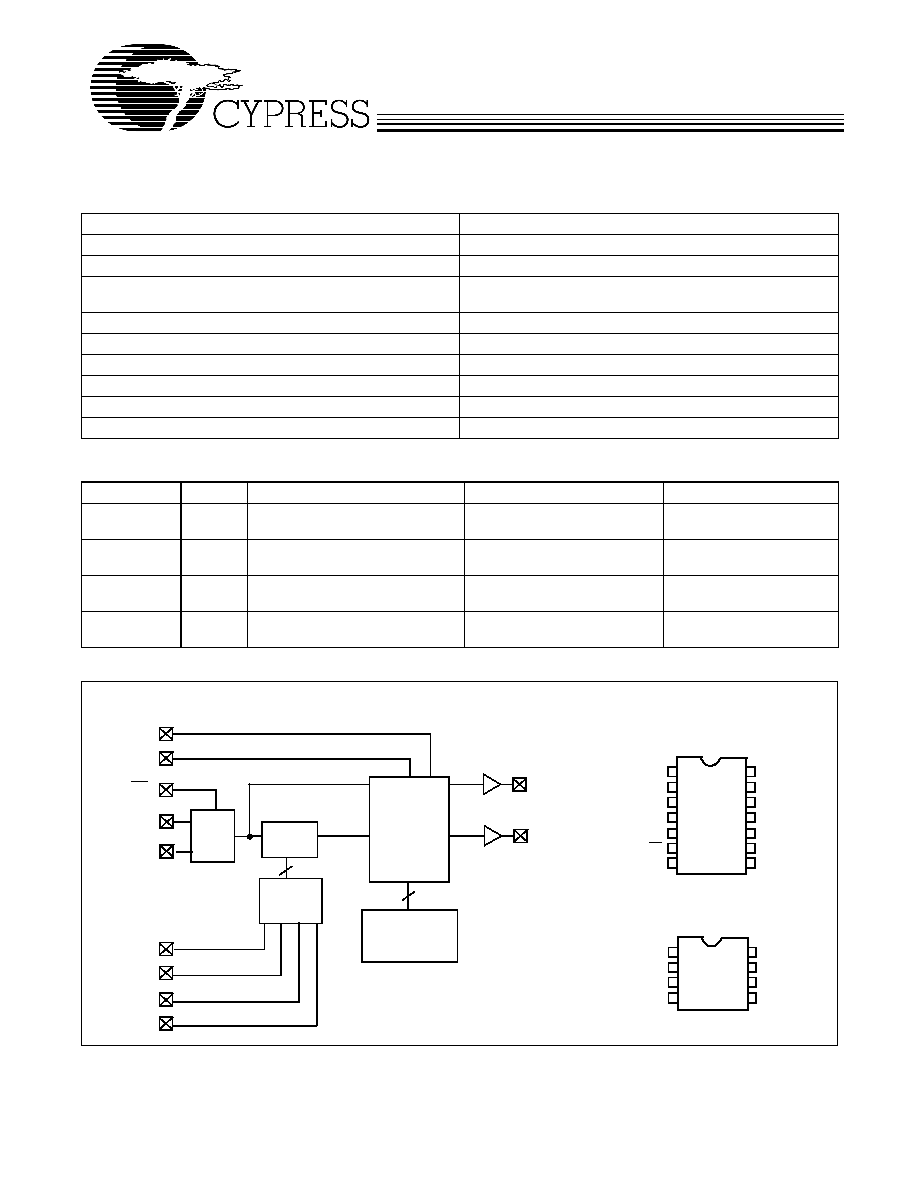
Features
Benefits
Single phase-locked loop architecture
Generates a custom frequency from an external source
EPROM programmability
Easy customization and fast turnaround
Factory-programmable (CY2907, CY2907I) or field-pro-
grammable (CY2907F & CY2907FI) device options
Programming support available for all opportunities
Up to two configurable outputs
Provides clocking requirements from a single device
Low-skew, low-jitter, high-accuracy outputs
Meets critical industry standard timing requirements
Power management (Power-Down, OE)
Supports low-power applications
Frequency select option
Up to 16 user-selectable frequencies
Configurable 5V or 3.3V operation
Supports industry-standard design platforms
8-pin or 14-pin SOIC packages
Industry-standard packaging saves on board space
Selector Guide
Part Number
Outputs
Input Frequency Range
Output Frequency Range
Specifics
CY2907
2
10 MHz25 MHz (external crystal)
1 MHz30 MHz (reference clock)
500 kHz130 MHz (5V)
500 kHz100 MHz (3.3V)
Factory Programmable
Commercial Temperature
CY2907I
2
10 MHz25 MHz (external crystal)
1 MHz30 MHz (reference clock)
500 kHz100 MHz (5V)
500 kHz80 MHz (3.3V)
Factory Programmable
Industrial Temperature
CY2907F8
CY2907F14
2
10 MHz25 MHz (external crystal)
1 MHz30 MHz (reference clock)
500 kHz100 MHz (5V)
500 kHz80 MHz (3.3V)
Field Programmable
Commercial Temperature
CY2907F8I
CY2907F14I
2
10 MHz25 MHz (external crystal)
1 MHz30 MHz (reference clock)
500 kHz90 MHz (5V)
500 kHz66.66 MHz (3.3V)
Field Programmable
Industrial Temperature
XTALOUT
XTALIN
REFCLK
OSC.
1
2
3
4
5
6
7
10
9
8
11
14
13
12
Top View
S1
S2
S3
V
SS
V
SS
PD
XTALIN
S0
REFCLK
V
DD
CLKA
OEA
OER
XTALOUT
CLKA
PLL
EPROM
Table
S0
S1
14-Pin SOIC
S2
S3
OER
Output
Multiplexer
and
Dividers
PD
1
2
3
4
5
8
7
6
S0
V
SS
XTALIN
XTALOUT
REFCLK
V
DD
CLKA
S1
8-Pin SOIC
Configuration
EPROM
and Test Logic
OEA
Logic Block Diagram
Pin Configurations
CY2907
Document #: 38-07137 Rev. **
Page 2 of 10
Functional Description
The CY2907 is a general-purpose Clock Generator designed
for use in a wide variety of applications--from graphics to PC
peripherals to disk drives. It generates selectable system clock
frequencies from a single reference input (crystal or reference
clock). The CY2907 is configured with an EPROM array, much
like the other devices in the Cypress EPROM Programmable
Clock Family, making it easily customizable for any applica-
tion. Furthermore, the CY2907 is compatible with all indus-
try-standard 9107 and 9108 clock synthesizers.
CyClocksTM Software
CyClocks is an easy-to-use software application that allows
you to configure any one of the EPROM Programmable Clocks
offered by Cypress. You may specify the input frequency, PLL
and output frequencies, and different functional options.
Please note the output frequency ranges in this data sheet
when specifying them in CyClocks to ensure that you stay
within the limits. You can download a copy of CyClocks free on
the Cypress Semiconductor website at www.cypress.com.
Consider using the CY2081, CY2291, or CY2292 for applica-
tions that require unrelated and multiple output frequencies.
Consider using the CY2071A for applications that require
more than one output clock.
Cypress FTG Programmer
The Cypress Frequency Timing Generator (FTG) Program-
mers are portable programmers designed to custom program
our family of EPROM Field Programmable Clock Devices.
The FTG programmers connect to a PC serial port and allow
users of CyClocks software to quickly and easily program any
of the CY2291F, CY2292F, CY2071AF, and CY2907F devices.
The ordering code for the Cypress FTG Programmer is
CY3670.
Maximum Ratings
(Beyond which the useful life may be impaired. For user guide-
lines, not tested.)
Supply Voltage ................................................. 0.5 to +7.0V
Input Voltage ........................................... 0.5V to V
DD
+0.5V
Storage Temperature (Non-Condensing) ... 65°C to +150°C
Max. Soldering Temperature (10 sec) ...................... +260°C
Junction Temperature ............................................... +150°C
Static Discharge Voltage ........................................... >2000V
(per MIL-STD-883, Method 3015)
Pin Summary
Name
Pin Number
Description
14-Pin SOIC
8-Pin SOIC
S1
1
5
Frequency Select (CLKA) (Internal pull-up resistor to V
DD
)
S2
2
NA
Frequency Select (CLKA) (Internal pull-up resistor to V
DD
)
S3
3
NA
Frequency Select (CLKA) (Internal pull-up resistor to V
DD
)
V
SS
4
2
Ground
V
SS
5
NA
Ground
PD
6
NA
Power-Down (active LOW) (Internal pull-up resistor to V
DD
)
XTALIN
[1]
7
3
Reference Crystal Input
XTALOUT
[1, 2]
8
4
Reference Crystal Feedback
OER
9
NA
REFCLK Output Enable (active HIGH) (Internal pull-up resistor to V
DD
)
OEA
10
NA
CLKA Output Enable (active HIGH) (Internal pull-up resistor to V
DD
)
CLKA
11
6
Clock Output
V
DD
12
7
Voltage Supply
REFCLK
13
8
Reference Clock Output (Default, can be driven by PLL if desired)
S0
14
1
Frequency Select (CLKA) (Internal pull-up resistor to V
DD
)
Notes:
1.
For best accuracy, use a parallel-resonant crystal, C
LOAD
17 pF.
2.
Float XTALOUT pin if XTALIN is driven by reference clock (as opposed to crystal).
CY2907
Document #: 38-07137 Rev. **
Page 3 of 10
Operating Conditions
[3]
Parameter
Description
Min.
Max.
Unit
V
DD
Supply Voltage, 5V Operation
4.5
5.5
V
Supply Voltage, 3.3V Operation
3.0
3.6
V
T
A
Commercial Operating Temperature, Ambient
0
70
°C
Industrial Operating Temperature, Ambient
40
85
°C
C
L
Max. Capacitive Load
15
pF
f
REF
External Reference Crystal
10.0
25.0
MHz
External Reference Clock
[4, 5]
1.0
30.0
MHz
Electrical Characteristics at 5.0V Commercial
V
DD
= 4.5V to 5.5V, T
A
= 0°C to +70°C
Parameter
Description
Test Conditions
Min.
Max.
Unit
V
IH
High-level Input Voltage
Except Crystal Inputs
2.0
V
V
IL
Low-level Input Voltage
Except Crystal Inputs
0.8
V
V
OH
[4]
High-level Output Voltage
V
DD
= V
DD
Min.
I
OH
= 30 mA
CLKA
2.4
V
V
OL
[4]
Low-level Output Voltage
V
DD
= V
DD
Min.
I
OL
= 10 mA
CLKA
0.4
V
I
OH
[4]
Output High Current
V
OH
= 2.0V
35
mA
I
OL
[4]
Output Low Current
V
OL
= 0.8V
22
mA
I
IH
Input High Current
V
IH
= V
DD
2
2
µ
A
I
IL
Input Low Current
V
IL
= 0V
20
µ
A
I
DD
[5]
Power Supply Current
PD HIGH, CLKA = 50 MHz
42
mA
I
DD
Power Supply Current
PD LOW, Logic Inputs LOW
100
µ
A
I
DD
Power Supply Current
PD LOW, Logic Inputs HIGH
40
µ
A
R
PU
[4]
Pull-up Resistor
V
IN =
V
DD
1.0 V
700
k
Electrical Characteristics at 3.3V Commercial
V
DD
= 3.0V to 3.6V, T
A
= 0°C to +70°C
Parameter
Description
Test Conditions
Min.
Max.
Unit
V
IH
High-level Input Voltage
Except Crystal Inputs
0.7*V
DD
V
V
IL
Low-level Input Voltage
Except Crystal Inputs
0.2*V
DD
V
V
OH
[4]
High-level Output Voltage
CLKA, I
OH
=
5 mA
0.85*V
DD
V
V
OL
[4]
Low-level Output Voltage
CLKA, I
OL
= 6 mA
0.1*V
DD
V
I
OH
[4]
Output High Current
V
OH
= 0.7*V
DD
10
mA
I
OL
[4]
Output Low Current
V
OL
= 0.2*V
DD
15
mA
I
IH
Input High Current
V
IH
= V
DD
2
2
µ
A
I
IL
Input Low Current
V
IL
= 0V
10
µ
A
I
DD
[5]
Power Supply Current
PD HIGH, CLKA = 50 MHz
40
mA
I
DD
Power Supply Current
PD LOW, Logic Inputs LOW
40
µ
A
I
DD
Power Supply Current
PD LOW, Logic Inputs HIGH
12
µ
A
R
PU
[4]
Pull-up Resistor
V
IN =
V
DD
0.5V
900
k
Notes:
3.
Electrical parameters are guaranteed with these operating conditions.
4.
Guaranteed by design, not 100% tested in production.
5.
Load = max. typical configuration, f
REF
= 14.318 MHz. Specific configurations may vary. A close approximation of I
DD
can be derived by the following formula:
I
DD
(mA) = V
DD
* (6.25 + (0.055*F
REF
) + (0.0017*C
LOAD
*(F
CLKA
+ REFCLK))). C
LOAD
is specified in pF and F is specified in MHz.
CY2907
Document #: 38-07137 Rev. **
Page 4 of 10
Electrical Characteristics at 5.0V Industrial
V
DD
= 4.5V to 5.5V, T
A
= 40°C to +85°C
Parameter
Description
Test Conditions
Min.
Max.
Unit
V
IH
High-level Input Voltage
Except Crystal Inputs
2.0
V
V
IL
Low-level Input Voltage
Except Crystal Inputs
0.8
V
V
OH
[4]
High-level Output Voltage
V
DD
= V
DD
Min. I
OH
= 30 mA
CLKA
2.4
V
V
OL
[4]
Low-level Output Voltage
V
DD
= V
DD
Min. I
OL
= 10 mA
CLKA
0.4
V
I
OH
[4]
Output High Current
V
OH
= 2.0V
45
mA
I
OL
[4]
Output Low Current
V
OL
= 0.8V
20
mA
I
IH
Input High Current
V
IH
= V
DD
2
2
µ
A
I
IL
Input Low Current
V
IL
= 0V
20
µ
A
I
DD
[5]
Power Supply Current
PD HIGH, CLKA = 50 MHz
54
mA
I
DD
Power Supply Current
PD LOW, Logic Inputs LOW
110
µ
A
I
DD
Power Supply Current
PD LOW, Logic Inputs HIGH
45
µ
A
R
PU
[4]
Pull-up Resistor
V
IN =
V
DD
1.0 V
700
k
Electrical Characteristics at 3.3V Industrial
V
DD
= 3.0V to 3.6V, T
A
= 40°C to +85°C
Parameter
Description
Test Conditions
Min.
Max.
Unit
V
IH
High-level Input Voltage
Except Crystal Inputs
0.7*V
DD
V
V
IL
Low-level Input Voltage
Except Crystal Inputs
0.2*V
DD
V
V
OH
[4]
High-level Output Voltage
CLKA, I
OH
=
5 mA
0.85*V
DD
V
V
OL
[4]
Low-level Output Voltage
CLKA, I
OL
= 6 mA
0.1*V
DD
V
I
OH
[4]
Output High Current
V
OH
= 0.7*V
DD
12
mA
I
OL
[4]
Output Low Current
V
OL
= 0.2*V
DD
14
mA
I
IH
Input High Current
V
IH
= V
DD
2
2
µ
A
I
IL
Input Low Current
V
IL
= 0V
10
µ
A
I
DD
[5]
Power Supply Current
PD HIGH, CLKA = 50 MHz
50
mA
I
DD
Power Supply Current
PD LOW, Logic Inputs LOW
50
µ
A
I
DD
Power Supply Current
PD LOW, Logic Inputs HIGH
15
µ
A
R
PU
[4]
Pull-up resistor
V
IN =
V
DD
0.5V
900
k
CY2907
Document #: 38-07137 Rev. **
Page 5 of 10
Switching Characteristics at 5.0V Commercial
[4]
Parameter
Output
[6]
Description
Test Conditions
Min.
Max.
Unit
t
R
CLKA
Output Rise Time 0.8V to 2.0V
15-pF Load
1.40
ns
t
F
CLKA
Output Fall Time 2.0V to 0.8V
15-pF Load
1.00
ns
t
R
CLKA
Output Rise Time 20% to 80%
15-pF Load
3.5
ns
t
F
CLKA
Output Fall Time 80% to 20%
15-pF Load
2.5
ns
t
D
CLKA
Duty Cycle
15-pF Load at 1.4V
45.0
55.0
%
F
I
XTALIN
Input Frequency
Crystal Oscillator
10
25
MHz
F
I
XTALIN
Input Frequency
External Input Clock
[7]
1
30
MHz
F
O
CLKA
Output Frequency
CY2907, 15-pF Load
0.5
130.0
MHz
CY2907F, 15-pF Load
0.5
100.0
MHz
t
JIS
CLKA
Jitter (One Sigma)
20 MHz to 130 MHz
150
ps
t
JIS
CLKA
Jitter (One Sigma)
14 MHz to 20 MHz
200
ps
t
JIS
CLKA
Jitter (One Sigma)
Less than 14 MHz
1
%
t
JAB
CLKA
Jitter (Absolute)
20 MHz to 130 MHz
250
+ 250
ps
t
JAB
CLKA
Jitter (Absolute)
14 MHz to 20 MHz
500
+ 500
ps
t
JAB
CLKA
Jitter (Absolute)
Less than 14 MHz
3
%
t
PU
Power-up Time
18
ms
t
FT
CLKA
Transition Time
8 MHz to 66.6 MHz
13
ms
Switching Characteristics at 3.3V Commercial
[4]
Parameter
Output
[6]
Description
Test Conditions
Min.
Max.
Unit
t
R
CLKA
Output Rise Time 20% to 80%
15-pF Load
3.5
ns
t
F
CLKA
Output Fall Time 80% to 20%
15-pF Load
2.5
ns
t
D
CLKA
Duty Cycle
15-pF Load at 1.4V
40.0
53.0
%
F
I
XTALIN
Input Frequency
Crystal Oscillator
10
25
MHz
F
I
XTALIN
Input Frequency
External Input Clock
[7]
1
30
MHz
F
O
CLKA
Output Frequency
CY2907, 15-pF Load
0.5
100.0
MHz
CY2907F, 15-pF Load
0.5
80.0
MHz
t
JIS
CLKA
Jitter (One Sigma)
25 MHz to 100 MHz
150
ps
t
JIS
CLKA
Jitter (One Sigma)
14 MHz to 25 MHz
200
ps
t
JIS
CLKA
Jitter (One Sigma)
Less than 14 MHz
1
%
t
JAB
CLKA
Jitter (Absolute)
25 MHz to 120 MHz
250
+250
ps
t
JAB
CLKA
Jitter (Absolute)
14 MHz to 25 MHz
500
+500
ps
t
JAB
CLKA
Jitter (Absolute)
Less than 14 MHz
3
%
t
PU
Power-up Time
18
ms
t
FT
CLKA
Transition Time
8 MHz to 66.6 MHz
13
ms
Notes:
6.
REFCLK output can also be configured to be driven by the PLL, in which case the above characteristics are valid.
7.
Please refer to the application note "Crystal Oscillator Topics" when using an external reference clock as an input frequency source.
: