 | ÐлекÑÑоннÑй компоненÑ: CY29351 | СкаÑаÑÑ:  PDF PDF  ZIP ZIP |
Äîêóìåíòàöèÿ è îïèñàíèÿ www.docs.chipfind.ru
2.5V or 3.3V, 200-MHz, 9-Output Zero Delay Buffer
CY29351
Cypress Semiconductor Corporation
·
3901 North First Street
·
San Jose
,
CA 95134
·
408-943-2600
Document #: 38-07475 Rev. *A
Revised July 26, 2004
Features
· Output frequency range: 25 MHz to 200 MHz
· Input frequency range: 25 MHz to 200 MHz
· 2.5V or 3.3V operation
· Split 2.5V/3.3V outputs
· ±2.5% max Output duty cycle variation
· 9 Clock outputs: Drive up to 18 clock lines
· Two reference clock inputs: LVPECL or LVCMOS
· 150-ps max output-output skew
· Phase-locked loop (PLL) bypass mode
· Spread AwareTM
· Output enable/disable
· Pin-compatible with MPC9351
· Industrial temperature range: 40°C to +85°C
· 32-Pin 1.0-mm TQFP package
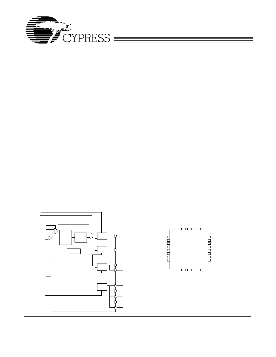
Functional Description
The CY29351 is a low voltage high performance 200 MHz
PLL-based zero delay buffer designed for high speed clock
distribution applications.
The CY29351 features LVPECL and LVCMOS reference clock
inputs and provides 9 outputs partitioned in 4 banks of 1, 1, 2,
and 5 outputs. Bank A divides the VCO output by 2 or 4 while
the other banks divide by 4 or 8 per SEL(A:D) settings, see
Functional Table. These dividers allow output to input ratios of
4:1, 2:1, 1:1, 1:2, and 1:4. Each LVCMOS compatible output
can drive 50
series or parallel terminated transmission lines.
For series terminated transmission lines, each output can
drive one or two traces giving the device an effective fanout of
1:18.
The PLL is ensured stable given that the VCO is configured to
run between 200 MHz to 500 MHz. This allows a wide range
of output frequencies from 25 MHz to 200 MHz. For normal
operation, the external feedback input, FB_IN, is connected to
one of the outputs. The internal VCO is running at multiples of
the input reference clock set by the feedback divider, see the
Table 1.
When PLL_EN is LOW, PLL is bypassed and the reference
clock directly feeds the output dividers. This mode is fully static
and the minimum input clock frequency specification does not
apply.
Block Diagram
Pin Configuration
Phase
Detector
LPF
÷2 / ÷4
÷4 / ÷8
÷4 / ÷8
÷4 / ÷8
QA
QB
QC0
QC1
QD0
QD1
QD2
QD3
QD4
SELA
PLL_EN
TCLK
REF_SEL
PECL_CLK
FB_IN
SELB
SELC
OE#
SELD
VCO
200 -
500 MHz
CY29351
R
E
F
_
SEL
PL
L_
EN
TC
LK
VSS
QA
VD
DQB
QB
VSS
PEC
L_
C
L
K#
OE
#
VD
D
QD
4
VS
S
QD
3
VDDQ
D
QD
2
Q C0
VD DQC
Q C1
VSS
Q D0
VD DQD
Q D1
VSS
AVDD
FB_IN
SELA
SELB
SELC
SELD
AVSS
PECL_CLK
1
2
3
4
5
6
7
8
24
23
22
21
20
19
18
17
9
10
11
12
13
14
15
16
32
31
30
29
28
27
26
25
CY29351
Document #: 38-07475 Rev. *A
Page 2 of 8
Pin Definitions
[1]
Pin
Name
I/O
Type
Description
8
PECL_CLK
I, PU
LVPECL
LVPECL reference clock input
9
PECL_CLK# I, PU/PD
LVPECL
LVPECL reference clock input. Weak pull-up to VDD/2.
30
TCLK
I, PD
LVCMOS LVCMOS/LVTTL reference clock input
28
QA
O
LVCMOS Clock output bank A
26
QB
O
LVCMOS Clock output bank B
22, 24
QC(1,0)
O
LVCMOS Clock output bank C
12, 14, 16,
18, 20
QD(4:0)
O
LVCMOS Clock output bank D
2
FB_IN
I, PD
LVCMOS Feedback clock input. Connect to an output for normal operation. This
input should be at the same voltage rail as input reference clock. See
Table 1.
10
OE#
I, PD
LVCMOS Output enable/disable input. See Table 2.
31
PLL_EN
I, PU
LVCMOS PLL enable/disable input. See Table 2.
32
REF_SEL
I, PD
LVCMOS Reference select input. See Table 2.
3, 4, 5, 6
SEL(A:D)
I, PD
LVCMOS Frequency select input, Bank (A:D). See Table 2.
27
VDDQB
Supply
VDD
2.5V or 3.3V Power supply for bank B output clock
[2,3]
23
VDDQC
Supply
VDD
2.5V or 3.3V Power supply for bank C output clocks
[2,3]
15, 19
VDDQD
Supply
VDD
2.5V or 3.3V Power supply for bank D output clocks
[2,3]
1
AVDD
Supply
VDD
2.5V or 3.3V Power supply for PLL
[2,3]
11
VDD
Supply
VDD
2.5V or 3.3V Power supply for core, inputs, and bank A output
clock
[2,3]
7
AVSS
Supply
Ground
Analog ground
13, 17, 21,
25, 29
VSS
Supply
Ground
Common ground
Table 1. Frequency Table
Feedback Output Divider
VCO
Input Frequency Range
(AVDD = 3.3V)
Input Frequency Range
(AVDD = 2.5V)
÷2
Input Clock * 2
100 MHz to 200 MHz
100 MHz to 190MHz
÷4
Input Clock * 4
50 MHz to 125 MHz
50 MHz to 95MHz
÷8
Input Clock * 8
25 MHz to 62.5 MHz
25 MHz to 47.5MHz
Table 2. Function Table
Control
Default
0
1
REF_SEL
0
PCLK
TCLK
PLL_EN
1
Bypass mode, PLL disabled. The input
clock connects to the output dividers
PLL enabled. The VCO output connects to the
output dividers
OE#
0
Outputs enabled
Outputs disabled (three-state), VCO running at
its minimum frequency
SELA
0
÷ 2 (Bank A)
÷ 4 (Bank A )
SELB
0
÷ 4 (Bank B)
÷ 8 (Bank B)
SELC
0
÷ 4 (Bank C)
÷ 8 (Bank C)
SELD
0
÷ 4 (Bank D)
÷ 8 (Bank D)
Notes:
1.
PU = Internal pull-up, PD = Internal pull-down.
2.
A 0.1-
µF bypass capacitor should be placed as close as possible to each positive power pin (<0.2"). If these bypass capacitors are not close to the pins their
high-frequency filtering characteristics will be cancelled by the lead inductance of the traces.
3.
AVDD and VDD pins must be connected to a power supply level that is at least equal or higher than that of VDDQB, VDDQC, and VDDQD power supply pins.
CY29351
Document #: 38-07475 Rev. *A
Page 3 of 8
Absolute Maximum Conditions
Parameter
Description
Condition
Min.
Max.
Unit
V
DD
DC Supply Voltage
0.3
5.5
V
V
DD
DC Operating Voltage
Functional
2.375
3.465
V
V
IN
DC Input Voltage
Relative to V
SS
0.3
V
DD
+ 0.3
V
V
OUT
DC Output Voltage
Relative to V
SS
0.3
V
DD
+ 0.3
V
V
TT
Output termination Voltage
V
DD
÷ 2
V
LU
Latch-up Immunity
Functional
200
mA
R
PS
Power Supply Ripple
Ripple Frequency < 100 kHz
150
mVp-p
T
S
Temperature, Storage
Non Functional
65
+150
°C
T
A
Temperature, Operating Ambient
Functional
40
+85
°C
T
J
Temperature, Junction
Functional
+150
°C
Ø
JC
Dissipation, Junction to Case
Functional
42
°C/W
Ø
JA
Dissipation, Junction to Ambient
Functional
105
°C/W
ESD
H
ESD Protection (Human Body Model)
2000
Volts
FIT
Failure in Time
Manufacturing test
10
ppm
DC Electrical Specifications
(V
DD
= 2.5V ± 5%, T
A
= 40°C to +85°C)
Parameter
Description
Condition
Min.
Typ.
Max.
Unit
V
IL
Input Voltage, Low
LVCMOS
0.7
V
V
IH
Input Voltage, High
LVCMOS
1.7
V
DD
+0.3
V
V
PP
Peak-Peak Input Voltage
LVPECL
250
1000
mV
V
CMR
Common Mode Range
[4]
LVPECL
1.0
V
DD
0.6
V
V
OL
Output Voltage, Low
[5]
I
OL
= 15mA
0.6
V
V
OH
Output Voltage, High
[5]
I
OH
= 15mA
1.8
V
I
IL
Input Current, Low
[6]
V
IL
= V
SS
100
µA
I
IH
Input Current, High
[6]
V
IL
= V
DD
100
µA
I
DDA
PLL Supply Current
AVDD only
5
10
mA
I
DDQ
Quiescent Supply Current
All V
DD
pins except AVDD
7
mA
I
DD
Dynamic Supply Current
Outputs loaded @ 100 MHz
180
mA
Outputs loaded @ 200 MHz
210
C
IN
Input Pin Capacitance
4
pF
Z
OUT
Output Impedance
14
18
22
DC Electrical Specifications
(V
DD
= 3.3V ± 5%, T
A
= 40°C to +85°C)
Parameter
Description
Condition
Min.
Typ.
Max.
Unit
V
IL
Input Voltage, Low
LVCMOS
0.8
V
V
IH
Input Voltage, High
LVCMOS
2.0
V
DD
+ 0.3
V
V
PP
Peak-Peak Input Voltage
LVPECL
250
1000
mV
V
CMR
Common Mode Range
[4]
LVPECL
1.0
V
DD
0.6
V
V
OL
Output Voltage, Low
[5]
I
OL
= 24 mA
0.55
V
I
OL
= 12 mA
0.30
V
OH
Output Voltage, High
[5]
I
OH
= 24 mA
2.4
V
Notes:
4.
V
CMR
(DC) is the crossing point of the differential input signal. Normal operation is obtained when the crossing point is within the V
CMR
range and the input
swing is within the V
PP
(DC) specification.
5.
Driving one 50
parallel terminated transmission line to a termination voltage of V
TT
. Alternatively, each output drives up to two 50
series terminated
transmission lines.
6.
Inputs have pull-up or pull-down resistors that affect the input current.
CY29351
Document #: 38-07475 Rev. *A
Page 4 of 8
I
IL
Input Current, Low
[6]
V
IL
= V
SS
100
µA
I
IH
Input Current, High
[6]
V
IL
= V
DD
100
µA
I
DDA
PLL Supply Current
AVDD only
5
10
mA
I
DDQ
Quiescent Supply Current
All VDD pins except AVDD
7
mA
I
DD
Dynamic Supply Current
Outputs loaded @ 100 MHz
270
mA
Outputs loaded @ 200 MHz
300
C
IN
Input Pin Capacitance
4
pF
Z
OUT
Output Impedance
12
15
18
AC Electrical Specifications
(V
DD
= 2.5V ± 5%, T
A
= 40°C to +85°C)
[7]
Parameter
Description
Condition
Min.
Typ.
Max.
Unit
f
VCO
VCO Frequency
200
380
MHz
f
in
Input Frequency
÷2 Feedback
100
190
MHz
÷4 Feedback
50
95
÷8 Feedback
25
47.5
Bypass mode (PLL_EN = 0)
0
200
f
refDC
Input Duty Cycle
25
75
%
V
PP
Peak-Peak Input Voltage
LVPECL
500
1000
mV
V
CMR
Common Mode Range
[8]
LVPECL
1.2
V
DD
0.6
V
t
r
, t
f
TCLK Input Rise/FallTime
0.7V to 1.7V
1.0
ns
f
MAX
Maximum Output Frequency
÷2 Output
100
190
MHz
÷4 Output
50
95
÷8 Output
25
47.5
DC
Output Duty Cycle
f
MAX
< 100 MHz
47.5
52.5
%
f
MAX
> 100 MHz
45
55
t
r
, t
f
Output Rise/Fall times
0.6V to 1.8V
0.1
1.0
ns
t
(
)
Propagation Delay (static phase
offset)
TCLK to FB_IN
100
100
ps
PCLK to FB_IN
100
100
t
sk(O)
Output-to-Output Skew
150
ps
t
PLZ, HZ
Output Disable Time
10
ns
t
PZL, ZH
Output Enable Time
10
ns
BW
PLL Closed Loop Bandwidth
(3dB)
÷2 Feedback
2.2
MHz
÷4 Feedback
0.85
÷8 Feedback
0.6
t
JIT(CC)
Cycle-to-Cycle Jitter
Same frequency
150
ps
Multiple frequencies
250
t
JIT(PER)
Period Jitter
Same frequency
100
ps
Multiple frequencies
175
t
JIT(
)
I/O Phase Jitter
175
ps
t
LOCK
Maximum PLL Lock Time
1
ms
Notes:
7.
AC characteristics apply for parallel output termination of 50
to V
TT
. Parameters are guaranteed by characterization and are not 100% tested.
8.
V
CMR
(AC) is the crosspoint of the differential input signal. Normal AC operation is obtained when the crosspoint is within the V
CMR
range and the input swing
lies within the V
PP
(AC) specification. Violation of V
CMR
or V
PP
impacts static phase offset t(
).
DC Electrical Specifications
(V
DD
= 3.3V ± 5%, T
A
= 40°C to +85°C) (continued)
Parameter
Description
Condition
Min.
Typ.
Max.
Unit
CY29351
Document #: 38-07475 Rev. *A
Page 5 of 8
AC Electrical Specifications
(V
DD
= 3.3V ± 5%, T
A
= 40°C to +85°C)
[7]
Parameter
Description
Condition
Min.
Typ.
Max.
Unit
f
VCO
VCO Frequency
200
500
MHz
f
in
Input Frequency
÷2 Feedback
100
200
MHz
÷4 Feedback
50
125
÷8 Feedback
25
62.5
Bypass mode (PLL_EN = 0)
0
200
f
refDC
Input Duty Cycle
25
75
%
V
PP
Peak-Peak Input Voltage
LVPECL
500
1000
mV
V
CMR
Common Mode Range
[8]
LVPECL
1.2
V
DD
0.9
V
t
r
, t
f
TCLK Input Rise/FallTime
0.8V to 2.0V
1.0
ns
f
MAX
Maximum Output Frequency
÷2 Output
100
200
MHz
÷4 Output
50
125
÷8 Output
25
62.5
DC
Output Duty Cycle
f
MAX
< 100 MHz
47.5
52.5
%
f
MAX
> 100 MHz
45
55
t
r
, t
f
Output Rise/Fall times
0.8V to 2.4V
0.1
1.0
ns
t
(
)
Propagation Delay (static phase
offset)
TCLK to FB_IN, same VDD
100
100
ps
PCLK to FB_IN, same VDD
100
100
t
sk(O)
Output-to-Output Skew
Banks at same voltage
150
ps
tsk(B)
Bank-to-Bank Skew
Banks at different voltages
350
ps
t
PLZ, HZ
Output Disable Time
10
ns
t
PZL, ZH
Output Enable Time
10
ns
BW
PLL Closed Loop Bandwidth
(3dB)
÷2 Feedback
2.2
MHz
÷4 Feedback
0.85
÷8 Feedback
0.6
t
JIT(CC)
Cycle-to-Cycle Jitter
Same frequency
150
ps
Multiple frequencies
250
t
JIT(PER)
Period Jitter
Same frequency
100
ps
Multiple frequencies
150
t
JIT(
)
I/O Phase Jitter
I/O same V
DD
175
ps
t
LOCK
Maximum PLL Lock Time
1
ms
P u ls e
G e n e ra to r
Z = 5 0 o h m
Z o = 5 0 o h m
V T T
Z o = 5 0 o h m
V T T
R
T
= 5 0 o h m
R
T
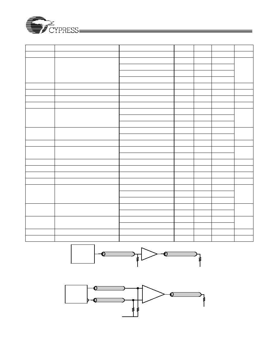
= 5 0 o h m
Figure 1. LVCMOS_CLK AC Test Reference for V
DD
= 3.3V / 2.5V
D iffe re n tia l
P u ls e
G e n e ra to r
Z = 5 0 o h m
Z o = 5 0 o h m
Z o = 5 0 o h m
V T T
R
T
= 5 0 o h m
Z o = 5 0 o h m
R
T
= 5 0 o h m
V T T
Figure 2. PECL_CLK AC Test Reference for V
DD
= 3.3V / 2.5V