 | –≠–ª–µ–∫—Ç—Ä–æ–Ω–Ω—ã–π –∫–æ–º–ø–æ–Ω–µ–Ω—Ç: CY29940-1 | –°–∫–∞—á–∞—Ç—å:  PDF PDF  ZIP ZIP |
2.5V or 3.3V, 200-MHz
1:18 Clock Distribution Buffer
CY29940-1
Cypress Semiconductor Corporation
∑
3901 North First Street
∑
San Jose
,
CA 95134
∑
408-943-2600
Document #: 38-07487 Rev. **
Revised January 28, 2003
Features
∑ 200-MHz clock support
∑ LVPECL or LVCMOS/LVTTL clock input
∑ LVCMOS/LVTTL-compatible inputs
∑ 18 clock outputs: drive up to 36 clock lines
∑ 150 ps max. output-to-output skew
∑ 23
output impedance
∑ Dual or single supply operation:
-- 3.3V core and 3.3V outputs
-- 3.3V core and 2.5V outputs
-- 2.5V core and 2.5V outputs
∑ Pin-compatible with MPC940L, MPC9109
∑ Available in commercial and industrial temperature
ranges
∑ 32-pin TQFP package
Description
The CY29940-1 is a low-voltage 200-MHz clock distribution
buffer with the capability to select either a differential LVPECL-
or a LVCMOS/LVTTL-compatible input clock. The two clock
sources can be used to provide for a test clock as well as the
primary system clock. All other control inputs are
LVCMOS/LVTTL-compatible. The eighteen outputs are 2.5V
or 3.3V LVCMOS/LVTTL-compatible and can drive 50
series
or parallel terminated transmission lines. For series terminated
transmission lines, each output can drive one or two traces
giving the device an effective fanout of 1:36. Low
output-to-output skews make the CY29940-1 an ideal clock
distribution buffer for nested clock trees in the most
demanding of synchronous systems.
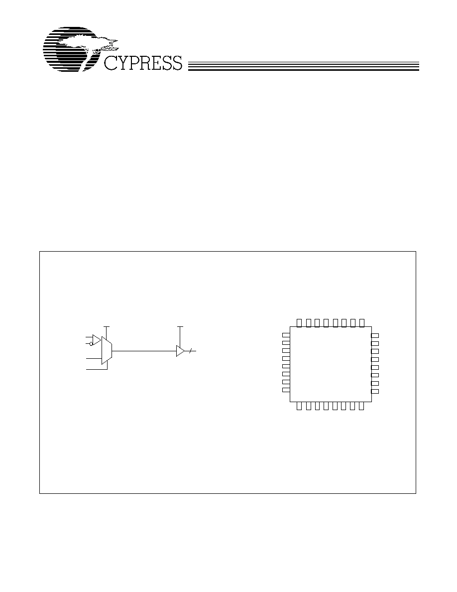
Block Diagram
Pin Configuration
PECL_CLK
PECL_CLK#
0
1
TCLK
TCLK_SEL
VDDC
18
Q0-Q17
VDD
CY29940-1
1
2
3
4
5
6
7
8
16
15
14
13
12
11
10
9
Q1
7
Q1
5
Q1
6
VS
S
Q1
4
Q1
3
Q1
2
VDD
C
24
23
22
21
20
19
18
17
Q6
Q8
Q7
VDD
Q9
Q10
Q11
VSS
25
26
27
28
29
30
31
32
Q0
Q2
Q1
VD
DC
Q3
Q4
Q5
VS
S
VSS
TCLK
VSS
TCLK_SEL
PECL_CLK
PECL_CLK#
VDD
VDDC
CY29940-1
Document #: 38-07487 Rev. **
Page 2 of 7
Note:
1.
PD = Internal Pull-down; PU = Internal Pull-up.
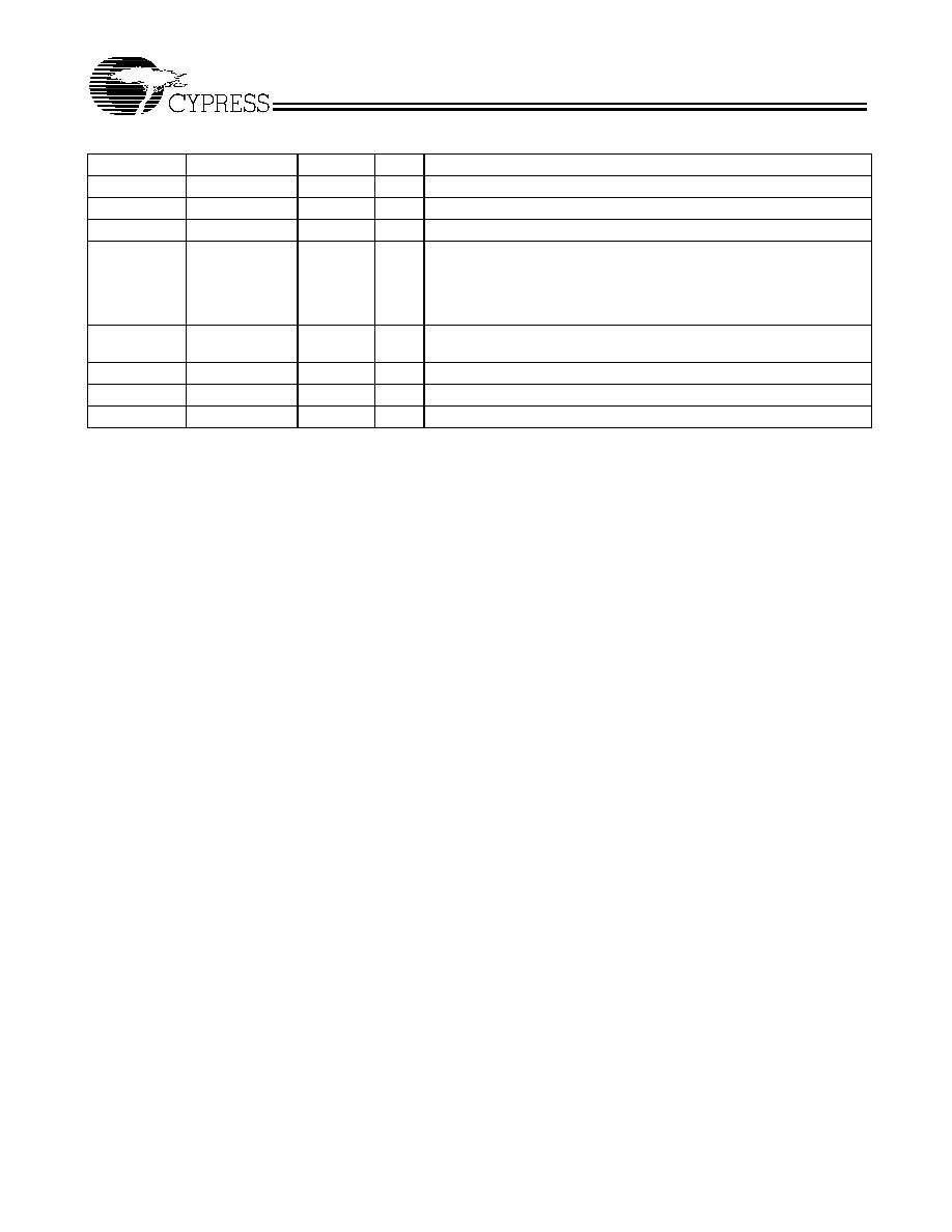
Pin Description
[1]
Pin
Name
PWR
I/O
Description
5
PECL_CLK
I, PU PECL Input Clock
6
PECL_CLK#
I, PD PECL Input Clock
3
TCLK
I, PD External Reference/Test Clock Input
9, 10, 11, 13,
14, 15, 18, 19,
20, 22, 23, 24,
26, 27, 28, 30,
31, 32
Q(17:0)
VDDC
O
Clock Outputs
4
TCLK_SEL
I, PD Clock Select Input. When LOW, PECL clock is selected and when HIGH
TCLK is selected.
8, 16, 29
VDDC
3.3V or 2.5V Power Supply for Output Clock Buffers
7, 21
VDD
3.3V or 2.5V Power Supply
1, 2, 12, 17, 25 VSS
Common Ground
CY29940-1
Document #: 38-07487 Rev. **
Page 3 of 7
Absolute Maximum Conditions
Maximum Input Voltage Relative to V
SS
: ............ V
SS
≠ 0.3V
Maximum Input Voltage Relative to V
DD
: ............. V
DD
+ 0.3V
Storage Temperature: ................................≠65
∞
C to + 150
∞
C
Operating Temperature: ................................ ≠40
∞
C to +85
∞
C
Maximum ESD Protection............................................... 2 kV
Maximum Power Supply: ................................................5.5V
Maximum Input Current: ............................................±20 mA
This device contains circuitry to protect the inputs against
damage due to high static voltages or electric field; however,
precautions should be taken to avoid application of any
voltage higher than the maximum rated voltages to this circuit.
For proper operation, V
in
and V
out
should be constrained to the
range:
V
SS
< (V
in
or V
out
) < V
DD
Unused inputs must always be tied to an appropriate logic
voltage level (either V
SS
or V
DD
).
Notes:
2.
Inputs have pull-up/pull-down resistors that effect input current.
3.
The VCMR is the difference from the most positive side of the differential input signal. Normal operation is obtained when the "High" input is within the VCMR
range and the input lies within the VPP specification. Driving series or parallel terminated 50
(or 50
to VDD/2) transmission lines.
4.
Outputs driving 50
transmission lines.
5.
See Figure 1 and Figure 2.
6.
50% input duty cycle.
DC Electrical Specifications:
V
DD
= 3.3V ±5% or 2.5V ±5%, V
DDC
= 3.3V ±5% or 2.5V ±5%
Parameter
Description
Conditions
Min.
Typ.
Max.
Unit
V
IL
Input Low Voltage
V
SS
0.8
V
V
IH
Input High Voltage
2.0
V
DD
V
I
IL
Input Low Current
[2]
≠200
µA
I
IH
Input High Current
[2]
200
µA
V
PP
Peak-to-Peak Input Voltage
PECL_CLK
500
1000
mV
V
CMR
Common Mode Range
[3]
PECL_CLK
V
DD
= 3.3V
V
DD
≠ 1.4
V
DD
≠ 0.6
V
V
DD
= 2.5V
V
DD
≠ 1.0
V
DD
≠ 0.6
V
OL
Output Low Voltage
[4,5,6]
I
OL
= 20 mA, V
DDC
= 3.3V
0.5
V
I
OL
= 16 mA, V
DDC
= 2.5V
V
OH
Output High Voltage
[4,5,6]
I
OH
= ≠20 mA, V
DDC
= 3.3V
2.4
V
I
OH
= ≠16 mA, V
DDC
= 2.5V
1.8
I
DDQ
Quiescent Supply Current
5
7
mA
I
DD
Dynamic Supply Current
V
DD
= 3.3V, Outputs @
150 MHz, CL=10 pF
285
mA
V
DD
= 3.3V, Outputs @
200 MHz, CL=10 pF
335
V
DD
= 2.5V, Outputs @
150 MHz, CL=10 pF
200
V
DD
= 2.5V, Outputs @
200 MHz, CL=10 pF
240
Z
out
Output Impedance
18
23
28
C
in
Input Capacitance
4
pF
CY29940-1
Document #: 38-07487 Rev. **
Page 4 of 7
Notes:
7.
Parameters are guaranteed by design and characterization. Not 100% tested in production. All parameters specified with loaded outputs.
8.
Across temperature and voltage ranges, includes output skew.
9.
For a specific temperature and voltage, includes output skew.
10. Parameters tested @ 150 MHz.
AC Electrical Specifications
(V
DD
= 3.3V ±5% or 2.5V ±5%, V
DDC
= 3.3V ±5% or 2.5V ±5%)
[7]
Parameter
Description
Conditions
Min.
Typ.
Max.
Unit
F
max
Input Frequency
LVCMOS Input
200
MHz
LVPECL Input
180
T
PD
PECL_CLK to Q Delay
[4,5,10]
</ =150 MHz
V
DD
= 3.3V
2.0
4.0
ns
V
DD
= 2.5V
2.6
5.2
LVCMOS to Q Delay
[4,5,10]
</ =150 MHz
V
DD
= 3.3V
1.8
3.4
V
DD
= 2.5V
2.3
4.0
FoutDC
Output Duty Cycle
[4,5,6]
FCLK < 134 MHz
45
55
%
FCLK > 134 MHz
40
60
T
skew
Output-to-Output Skew
[4,5]
150
ps
T
skew
(pp)
Part-to-Part Skew
[8]
PECL, V
DDC
= 3.3V
1.4
ns
PECL, V
DDC
= 2.5V
2.2
T
skew
(pp)
Part-to-Part Skew
[8]
TCLK, V
DDC
= 3.3V
1.2
ns
TCLK, V
DDC
= 2.5V
1.7
T
skew
(pp)
Part to Part Skew
[9]
PECL_CLK
850
ps
TCLK
750
t
R
/t
F
Output Clocks Rise/Fall Time
[4,5]
0.7V to 2.0V,
V
DDC
= 3.3V
0.3
1.1
ns
0.5V to 1.8V,
V
DDC
= 2.5V
0.3
1.3
Pulse
Generator
Z = 50 ohm
Zo = 50 ohm
VTT
Zo = 50 ohm
VTT
R
T
= 50 ohm
R
T
= 50 ohm
CY29940-1 DUT
Figure 1. LVCMOS_CLK CY29940-1 Test Reference for V
CC
= 3.3V and V
CC
= 2.5V
Differential
Pulse
Generator
Z = 50 ohm
Zo = 50 ohm
Zo = 50 ohm
VTT
R
T
= 50 ohm
CY29940-1 DUT
Zo = 50 ohm
R
T
= 50 ohm
VTT
Figure 2. PECL_CLK CY29940-1 Test Reference for V
CC
= 3.3V and V
CC
= 2.5V
CY29940-1
Document #: 38-07487 Rev. **
Page 5 of 7
t
PD
PECL_CLK
PECL_CLK
V
PP
Q
V
CMR
VCC
GND
VCC /2
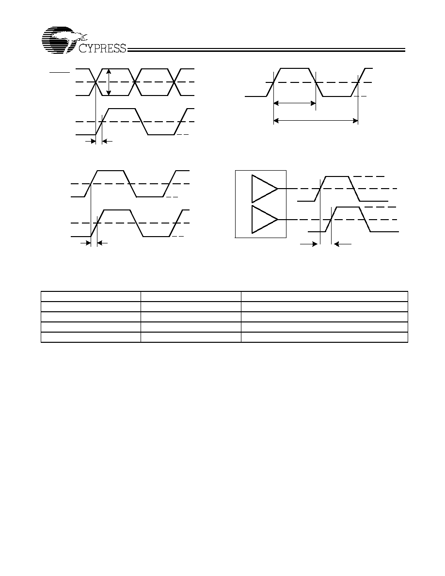
Figure 3. Propagation Delay (TPD) Test Reference
t
PD
LVCMOS_CLK
Q
VCC
GND
VCC /2
VCC
GND
VCC /2
Figure 4. LVCMOS Propagation Delay (TPD) Test
Reference
VCC
GND
VCC /2
t
P
T0
DC = tP / T0 x 100%
Figure 5. Output Duty Cycle (FoutDC)
t
SK(0)
VCC
GND
VCC /2
VCC
GND
VCC /2
Figure 6. Output-to-Output Skew tsk(0)
Ordering Information
Part Number
Package Type
Production Flow
CY29940AC≠1
32-pin TQFP
Commercial, 0∞C to 70∞C
CY29940AC≠1T
32-pin TQFP ≠ Tape and Reel
Commercial, 0∞C to 70∞C
CY29940AI≠1
32-pin TQFP
Industrial, ≠40∞C to +85∞C
CY29940AI≠1T
32-pin TQFP ≠ Tape and Reel
Industrial, ≠40∞C to +85∞C