 | ÐлекÑÑоннÑй компоненÑ: CY29942AI | СкаÑаÑÑ:  PDF PDF  ZIP ZIP |
Äîêóìåíòàöèÿ è îïèñàíèÿ www.docs.chipfind.ru
2.5V or 3.3V, 200-MHz, 1:18 Clock Distribution Buffer
CY29942
Cypress Semiconductor Corporation
·
3901 North First Street
·
San Jose
·
CA 95134
·
408-943-2600
Document #: 38-07284 Rev. *B
Revised December 21, 2002
42
Features
· 200-MHz clock support
· 2.5V or 3.3V operation
· LVCMOS/LVTTL clock input
· LVCMOS-/LVTTL-compatible inputs
· 18 clock outputs: drive up to 36 clock lines
· 200 ps max. output-to-output skew
· Output Enable control
· Pin compatible with MPC942C
· Available in Industrial and Commercial
· 32-pin LQFP package
Description
The CY29942 is a low-voltage 200-MHz clock distribution buff-
er with an LVCMOS or LVTTL compatible input clock. All other
control inputs are LVCMOS/LVTTL compatible. The eighteen
outputs are 2.5V or 3.3V LVCMOS or LVTTL compatible and
can drive 50
series or parallel terminated transmission lines.
For series terminated transmission lines, each output can
drive one or two traces giving the devices an effective fanout
of 1:36. Low output-to-output skews make the CY29942 an
ideal clock distribution buffer for nested clock trees in the most
demanding of synchronous systems.
Block Diagram
Pin Configuration
TCLK
OE
VDD
18
Q0-Q17
CY29942
Q0
Q1
Q2
VDD
Q3
Q4
Q5
VSS
Q17
Q16
Q15
VSS
Q14
Q13
Q12
VDD
Q6
Q7
Q8
VDD
Q9
Q10
Q11
VSS
VSS
VSS
TCLK
NC
OE
NC
VDD
VDD
1
2
3
4
5
6
7
8
24
23
22
21
20
19
18
17
9
10
11
12
13
14
15
16
32
31
30
29
28
27
26
25
CY29942
Document #: 38-07284 Rev. *B
Page 2 of 7
Note:
1.
PD = Internal Pull-Down, PU = Internal Pull-up.
Pin Description
[1]
Pin
Name
PWR
I/O
Description
3
TCLK
I, PD
External Reference/Test Clock Input
5
OE
I, PU
Output Enable. When HIGH, all the outputs are enabled. When set
LOW, the outputs are at high impedance.
9, 10, 11, 13,
14, 15, 18, 19,
20, 22, 23, 24,
26, 27, 28, 30,
31, 32
Q(17:0)
VDD
O
Clock Outputs
7, 8, 16, 21,
29
VDD
3.3V or 2.5V Power Supply
1, 2, 12, 17,
25
VSS
Common Ground
4, 6
NC
No Connection
CY29942
Document #: 38-07284 Rev. *B
Page 3 of 7
Maximum Ratings
[2]
Maximum Input Voltage Relative to V
SS
: ............. V
SS
0.3V
Maximum Input Voltage Relative to V
DD
: ............. V
DD
+ 0.3V
Storage Temperature: ................................ 65°C to + 150°C
Operating Temperature: ................................ 40°C to +85°C
Maximum ESD protection ............................................... 2 kV
Maximum Power Supply: ................................................5.5V
Maximum Input Current: ............................................±20 mA
This device contains circuitry to protect the inputs against
damage due to high static voltages or electric field; however,
precautions should be taken to avoid application of any volt-
age higher than the maximum rated voltages to this circuit. For
proper operation, V
in
and V
out
should be constrained to the
range:
V
SS
< (V
in
or V
out
) < V
DD
Unused inputs must always be tied to an appropriate logic volt-
age level (either V
SS
or V
DD
).
Notes:
2.
Multiple Supplies: The Voltage on any input or I/O pin cannot exceed the power pin during power-up. Power supply sequencing is NOT required.
3.
Inputs have pull-up/pull-down resistors that effect input current.
4.
Driving series or parallel terminated 50
(or 50
to VDD/2) transmission lines.
DC Parameters:
V
DD
= 3.3V ±5% or 2.5V ±5%, V
DDC
= 3.3V ±5% or 2.5V ±5%, Over the specified temperature range.
Parameter
Description
Conditions
Min.
Typ.
Max.
Unit
V
IL
Input Low Voltage
VSS
0.8
V
V
IH
Input High Voltage
2.0
VDD
V
I
IL
Input Low Current
[3]
200
µA
I
IH
Input High Current
[3]
200
µA
V
OL
Output Low Voltage
[4]
I
OL
= 20 mA
0.5
V
V
OH
Output High Voltage
[4]
I
OH
= 20 mA, V
DDC
= 3.3V
2.4
V
I
OH
= 16 mA, V
DDC
= 2.5V
2.0
I
DDQ
Quiescent Supply
Current
5
7
mA
I
DD
Dynamic Supply
Current
V
DD
= 3.3V, Outputs @ 150 MHz,
CL = 15 pF
285
mA
V
DD
= 3.3V, Outputs @ 200 MHz,
CL = 15 pF
335
V
DD
= 2.5V, Outputs @ 150 MHz,
CL = 15pF
200
V
DD
= 2.5V, Outputs @ 200 MHz,
CL = 15pF
240
Z
out
Output Impedance
V
DD
= 3.3V
8
12
16
V
DD
= 2.5V
10
15
20
C
in
Input Capacitance
4
pF
CY29942
Document #: 38-07284 Rev. *B
Page 4 of 7
Notes:
5.
Parameters are guaranteed by design and characterization. Not 100% tested in production. All parameters specified with loaded outputs.
6.
Outputs driving 50
transmission lines.
7.
See Figure 1.
8.
50% input duty cycle.
9.
Across temperature and voltage ranges, includes output skew.
10. For a specific temperature and voltage, includes output skew.
AC Parameters
[5]
: V
DD
= 3.3V ±5% or 2.5V ±5%, V
DDC
= 3.3V ±5% or 2.5V ±5%, Over the specified temperature range
Parameter
Description
Conditions
Min.
Typ.
Max.
Unit
Fmax
Input Frequency
200
MHz
Tpd
TTL_CLK to Q Delay
[6, 7]
V
DD
= 3.3V
1.8
3.3
3.8
ns
V
DD
= 2.5V
2.3
3.8
4.4
FoutDC
Output Duty Cycle
[6, 7, 8]
Measured at V
DD
/2
45
55
%
Tskew
Output-to-Output Skew
[6, 7]
200
ps
Tskew(pp)
Part-to-Part Skew
[9]
V
DD
= 3.3V
1.0
ns
V
DD
= 2.5V
1.3
Tskew(pp)
Part-to-Part Skew
[10]
600
ps
Tr/Tf
Output Clocks Rise/Fall
Time
[6, 7]
0.8V to 2.0V, V
DD
= 3.3V
0.2
1.1
ns
0.5V to 1.8V, V
DD
= 2.5V
Pulse
Generator
Z = 50 ohm
Zo = 50 ohm
VTT
Zo = 50 ohm
VTT
R
T
= 50 ohm
R
T
= 50 ohm
CY29942 DUT
Figure 1. LVCMOS_CLK CY29942 Test Reference for V
CC
= 3.3V and V
CC
= 2.5V
t
PD
LVCMOS_CLK
Q
VCC
GND
VCC /2
VCC
GND
VCC /2
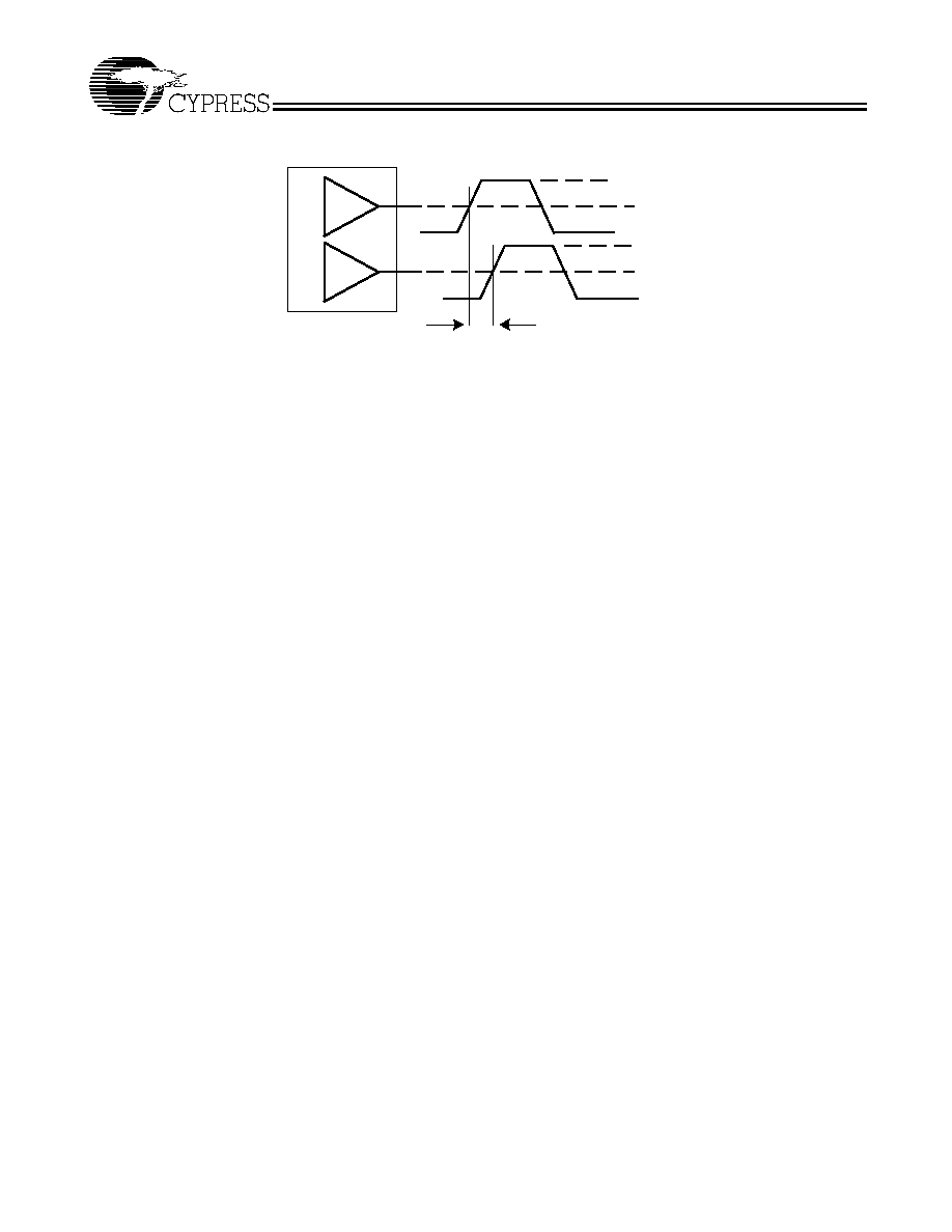
Figure 2. LVCMOS Propagation Delay (TPD) Test Reference
VCC
GND
VCC /2
t
P
T0
DC = tP / T0 x 100%
Figure 3. Output Duty Cycle (FoutDC)
CY29942
Document #: 38-07284 Rev. *B
Page 5 of 7
t
SK(0)
VCC
GND
VCC /2
VCC
GND
VCC /2
Figure 4. Output-to-Output Skew tsk(0)