 | ÐлекÑÑоннÑй компоненÑ: CY29946AI | СкаÑаÑÑ:  PDF PDF  ZIP ZIP |
/home/web/doc/html/cypress/169310
2.5V or 3.3V, 200-MHz, 1:10 Clock Distribution Buffer
CY29946
Cypress Semiconductor Corporation
·
3901 North First Street
·
San Jose
·
CA 95134
·
408-943-2600
Document #: 38-07286 Rev. *B
Revised December 22, 2002
46
Features
· 2.5V or 3.3V operation
· 200-MHz clock support
· 2 LVCMOS-/LVTTL-compatible inputs
· 10 clock outputs: drive up to 20 clock lines
· 1X or 1/2X configurable outputs
· Output three-state control
· 250 ps max. output-to-output skew
· Pin compatible with MPC946, MPC9446
· Available in Commercial and Industrial temp. range
· 32-pin TQFP package
Description
The CY29946 is a low-voltage 200-MHz clock distribution buff-
er with the capability to select one of two LVCMOS/LVTTL
compatible input clocks. These clock sources can be used to
provide for test clocks as well as the primary system clocks.
All other control inputs are LVCMOS/LVTTL compatible. The
10 outputs are LVCMOS or LVTTL compatible and can drive
50
series or parallel terminated transmission lines. For series
terminated transmission lines, each output can drive one or
two traces giving the device an effective fanout of 1:20.
The CY29946 is capable of generating 1X and 1/2X signals
from a 1X source. These signals are generated and retimed
internally to ensure minimal skew between the 1X and 1/2X
signals. SEL(A:C) inputs allow flexibility in selecting the ratio
of 1X to1/2X outputs.
The CY29946 outputs can also be three-stated via MR/OE#
input. When MR/OE# is set HIGH, it resets the internal
flip-flops and three-states the outputs.
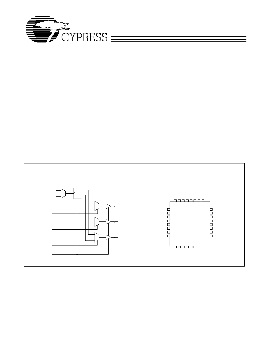
Block Diagram
Pin Configuration
3
QA0:2
3
QB0:2
4
QC0:3
0
1
0
1
0
1
0
1
/1
/2
R
TCLK0
TCLK_SEL
TCLK1
DSELA
DSELB
DSELC
MR/OE#
CY29946
MR/
O
E#
VSS
QA0
VDDC
QA1
VSS
QA2
VDDC
VDDC
QC0
VSS
QC1
VDDC
QC2
VSS
QC3
VSS
QB0
VDDC
QB1
VSS
QB2
VDDC
VDDC
TCLK_SEL
VDD
TCLK0
TCLK1
DSELA
DSELB
DSELC
VSS
1
2
3
4
5
6
7
8
24
23
22
21
20
19
18
17
9
10
11
12
13
14
15
16
32
31
30
29
28
27
26
25
CY29946
Document #: 38-07286 Rev. *B
Page 2 of 7
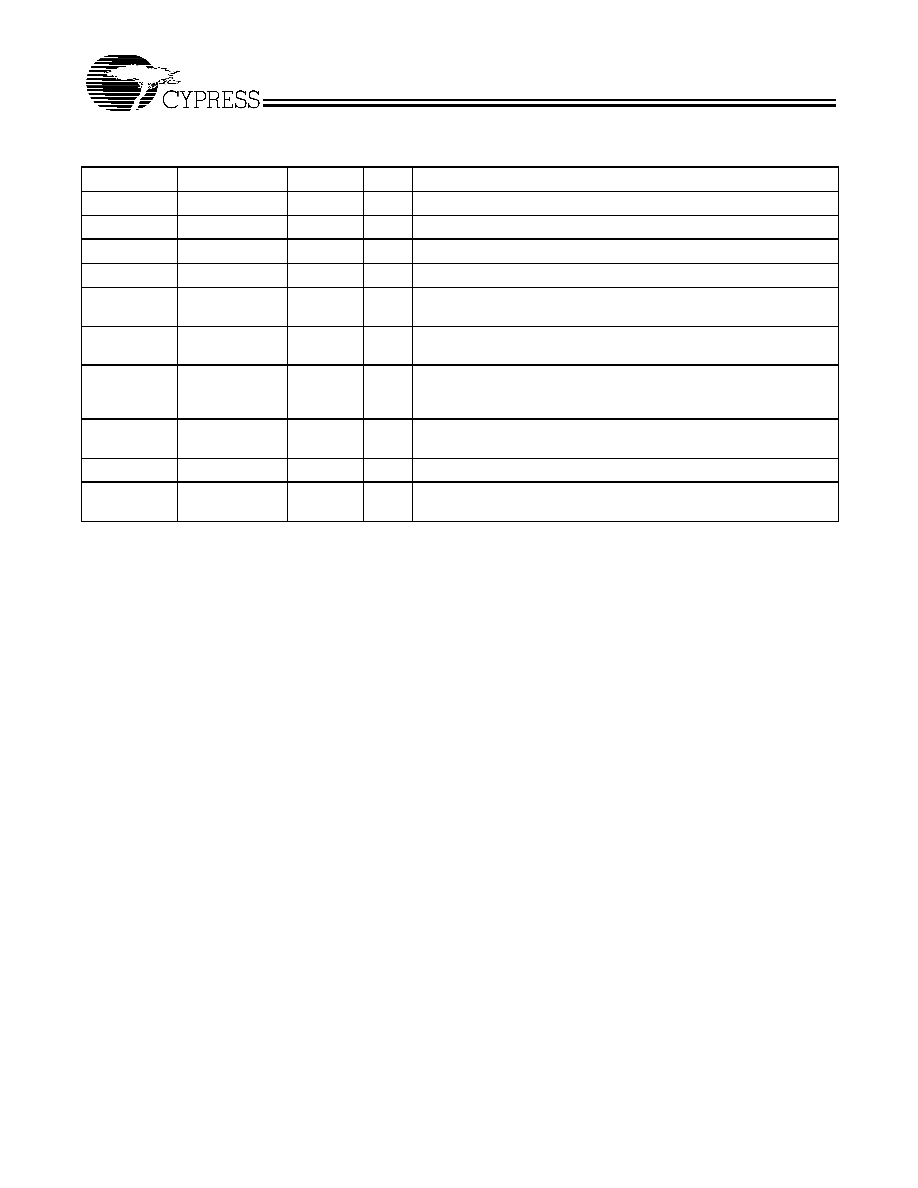
Note:
1.
PD = Internal Pull-Down, PU = Internal Pull- UP
Pin Description
[1]
Pin
Name
PWR
I/O
Description
3, 4
TCLK(0,1)
I, PU
External Reference/Test Clock Input
26, 28, 30
QA(2:0)
VDDC
O
Clock Outputs
19, 21, 23
QB(2:0)
VDDC
O
Clock Outputs
10, 12, 14, 16
QC(0:3)
VDDC
O
Clock Outputs
5, 6, 7
DSEL(A:C)
I, PD
Divider Select Inputs. When HIGH, selects ³2 input divider. When
LOW, selects ³1 input divider.
1
TCLK_SEL
I, PD
TCLK Select Input. When LOW, TCLK0 clock is selected and when
HIGH TCLK1 is selected.
32
MR/OE#
I, PD
Output Enable Input. When asserted LOW, the outputs are enabled
and when asserted HIGH, internal flip-flops are reset and the outputs
are three-stated.
9, 13, 17, 18,
22, 25, 29
VDDC
2.5V or 3.3V Power Supply for Output Clock Buffers
2
VDD
2.5V or 3.3V Power Supply
8, 11, 15, 20,
24, 27, 31
VSS
Common Ground
CY29946
Document #: 38-07286 Rev. *B
Page 3 of 7
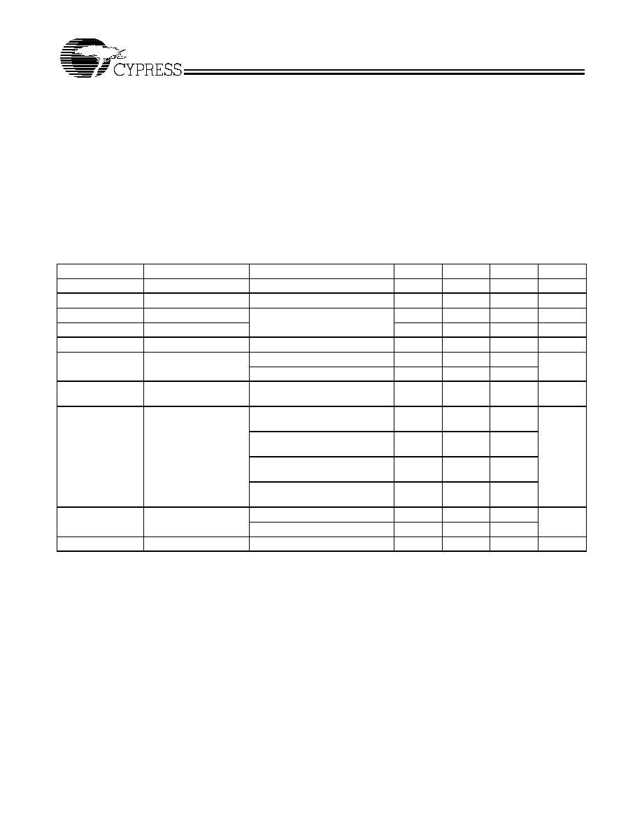
Maximum Ratings
[2]
Maximum Input Voltage Relative to V
SS
: ............. V
SS
0.3V
Maximum Input Voltage Relative to V
DD
: ............. V
DD
+ 0.3V
Storage Temperature: ................................ 65°C to + 150°C
Operating Temperature: ................................ 40°C to +85°C
Maximum ESD protection ............................................... 2 kV
Maximum Power Supply: ................................................5.5V
Maximum Input Current: .............................................±20mA
This device contains circuitry to protect the inputs against
damage due to high static voltages or electric field; however,
precautions should be taken to avoid application of any volt-
age higher than the maximum rated voltages to this circuit. For
proper operation, V
in
and V
out
should be constrained to the
range:
V
SS
< (V
in
or V
out
) < V
DD
Unused inputs must always be tied to an appropriate logic volt-
age level (either V
SS
or V
DD
).
Notes:
2.
Multiple Supplies: The voltage on any input or I/O pin cannot exceed the power pin during power-up. Power supply sequencing is NOT required.
3.
Inputs have pull-up/pull-down resistors that effect input current.
4.
Driving series or parallel terminated 50
(or 50
to V
DD
/2) transmission lines.
DC Parameters:
V
DD
= V
DDC
= 3.3V ±10% or 2.5V ±5%, Over the specified temperature range
Parameter
Description
Conditions
Min.
Typ.
Max.
Unit
V
IL
Input Low Voltage
V
SS
0.8
V
V
IH
Input High Voltage
2.0
V
DD
V
I
IL
Input Low Current
[3]
100
µA
I
IH
Input High Current
[3]
100
µA
V
OL
Output Low Voltage
[4]
I
OL
= 20 mA
0.4
V
V
OH
Output High Voltage
[4]
I
OH
= 20 mA, V
DD
= 3.3V
2.5
V
I
OH
= 20 mA, V
DD
= 2.5V
1.8
I
DDQ
Quiescent Supply
Current
5
7
mA
I
DD
Dynamic Supply
Current
V
DD
= 3.3V, Outputs @ 100 MHz,
CL = 30 pF
130
mA
V
DD
= 3.3V, Outputs @ 160 MHz,
CL = 30 pF
225
V
DD
= 2.5V, Outputs @ 100 MHz,
CL = 30 pF
95
V
DD
= 2.5V, Outputs @ 160 MHz,
CL = 30 pF
160
Z
Out
Output Impedance
V
DD
= 3.3V
12
15
18
V
DD
= 2.5V
14
18
22
C
in
Input Capacitance
4
pF
CY29946
Document #: 38-07286 Rev. *B
Page 4 of 7
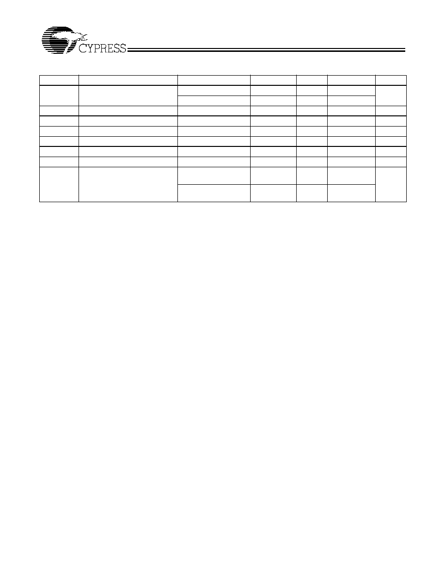
Notes:
5.
Parameters are guaranteed by design and characterization. Not 100% tested in production. All parameters specified with loaded outputs.
6.
Outputs driving 50
transmission lines.
7.
50% input duty cycle.
8.
See Figure 1.
9.
Part-to-Part skew at a given temperature and voltage.
AC Parameters
[5]
:
V
DD
= V
DDC
= 3.3V ±10% or 2.5V ±5%, Over the specified temperature range
Parameter
Description
Conditions
Min.
Typ.
Max.
Unit
Fmax
Input Frequency
[6]
V
DD
= 3.3V
200
MHz
V
DD
= 2.5V
170
Tpd
TTL_CLK To Q Delay
[6]
5.0
11.5
ns
FoutDC
Output Duty Cycle
[6, 7]
Measured at V
DD
/2
45
55
%
tpZL, tpZH
Output enable time (all outputs)
2
10
ns
tpLZ, tpHZ
Output disable time (all outputs)
2
10
ns
Tskew
Output-to-Output Skew
[6, 8]
150
250
ps
Tskew(pp)
Part-to-Part Skew
[9]
2.0
4.5
ns
Tr/Tf
Output Clocks Rise/Fall Time
[8]
0.8V to 2.0V,
V
DD
= 3.3V
0.10
1.0
ns
0.6V to 1.8V,
V
DD
= 2.5V
0.10
1.3
CY29946
Document #: 38-07286 Rev. *B
Page 5 of 7
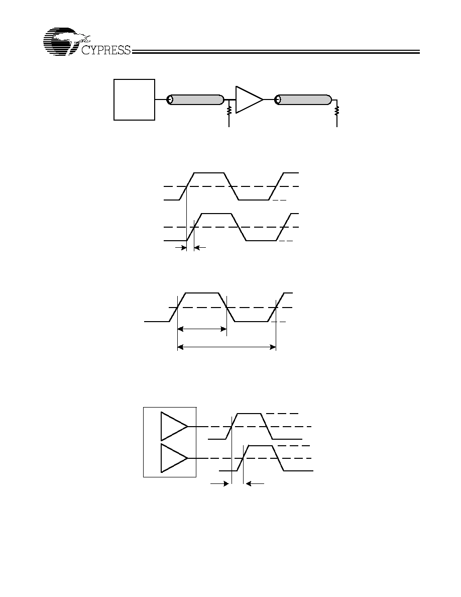
Pulse
Generator
Z = 50 ohm
Zo = 50 ohm
VTT
Zo = 50 ohm
VTT
R
T
= 50 ohm
R
T
= 50 ohm
CY29946 DUT
Figure 1. LVCMOS_CLK CY29946 Test Reference for V
CC
= 3.3V and V
CC
= 2.5V
t
PD
LVCMOS_CLK
Q
VCC
GND
VCC /2
VCC
GND
VCC /2
Figure 2. LVCMOS Propagation Delay (TPD) Test Reference
VCC
G N D
VC C /2
t
P
T0
D C = tP / T0 x 100%
Figure 3. Output Duty Cycle (FoutDC)
t
SK(0)
VCC
GND
VCC /2
VCC
GND
VCC /2
Figure 4. Output-to-Output Skew tsk(0)