 | –≠–ª–µ–∫—Ç—Ä–æ–Ω–Ω—ã–π –∫–æ–º–ø–æ–Ω–µ–Ω—Ç: CY29976AI | –°–∫–∞—á–∞—Ç—å:  PDF PDF  ZIP ZIP |

3.3V, 125-MHz, Multi-Output Zero Delay Buffer
CY29976
Cypress Semiconductor Corporation
∑
3901 North First Street
∑
San Jose
∑
CA 95134
∑
408-943-2600
Document #: 38-07413 Rev. *A
Revised December 27, 2002
76
Features
∑ Output frequency up to 125 MHz
∑ Supports PowerPC
Æ
, and Pentium
Æ
processors
∑ 12 clock outputs: frequency configurable
∑ Configurable Output Disable
∑ Two reference clock inputs for dynamic toggling
∑ Oscillator or PECL reference input
∑ Spread spectrum compatible
∑ Glitch-free output clocks transitioning
∑ 3.3V power supply
∑ Pin compatible with SC973X
∑ Industrial temperature range: ≠40∞C to +85∞C
∑ 52-Pin TQFP package
Note:
1.
x = the reference input frequency, 200MHz < F
VCO
< 480MHz
.
Table 1. Frequency Table
[1]
VC0_SEL
FB_SEL2
FB_SEL1
FB_SEL0
F
VCO
0
0
0
0
8x
0
0
0
1
12x
0
0
1
0
16x
0
0
1
1
20x
0
1
0
0
8x
0
1
0
1
12x
0
1
1
0
16x
0
1
1
1
20x
1
0
0
0
4x
1
0
0
1
6x
1
0
1
0
8x
1
0
1
1
10x
1
1
0
0
4x
1
1
0
1
6x
1
1
1
0
8x
1
1
1
1
10x
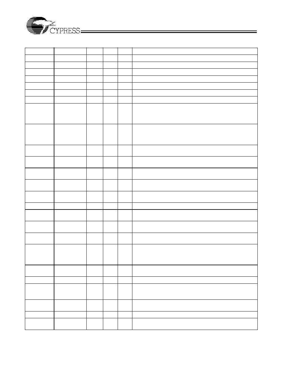
Block Diagram
Pin Configuration
VSS
MR#/OE
SCLK
SDATA
FB_SEL2
PLL_EN
REF_SEL
TCLK_SEL
TCLK0
TCLK1
PECL_CLK
PECL_CLK#
VDD
FB
_
S
E
L
1
SYN
C
VSS
QC
0
V
DDC
QC
1
SEL
C
0
SEL
C
1
QC
2
V
DDC
QC
3
VSS
IN
V
_
C
L
K
SEL
B1
SEL
B0
SEL
A1
SEL
A0
QA
3
V
DDC
QA
2
VSS
QA
1
V
DDC
QA
0
VSS
V
C
O_
SEL
VSS
Q B0
VDDC
Q B1
VSS
Q B2
VDDC
Q B3
FB_IN
VSS
FB_O UT
VDDC
FB_SEL0
1
2
3
4
5
6
7
8
9
10
11
12
13
39
38
37
36
35
34
33
32
31
30
29
28
27
14 15 16 17 18 19 20 21 22 23 24 25 26
52 51 50 49 48 47 46 45 44 43 42 41 40
CY29976
REF_SEL
0
1
0
1
Phase
Detector
VCO
LPF
Sync
Frz
D Q
QA0
Sync
Frz
D Q
Sync
Frz
D Q
Sync
Frz
D Q
Sync
Frz
D Q
Sync
Frz
D Q
Power-On
Reset
Output Disable
Circuitry
Data Generator
/2, /6, /4, /12
/2, /6, /4, /10
/8, /2, /6, /4
/4, /6, /8, /10
Sync Pulse
PECL_CLK
PECL_CLK#
TCLK0
TCLK1
TCLK_SEL
FB_IN
MR#/OE
SELA(0,1)
2
SELB(0,1)
2
SELC(0,1)
2
FB_SEL(0:2)
3
SCLK
SDATA
INV_CLK
QA1
QA2
QA3
QB0
QB1
QB2
QB3
QC0
QC1
QC2
QC3
FB_OUT
SYNC
12
VCO_SEL
PLL_EN
CY29976
Document #: 38-07413 Rev. *A
Page 2 of 10
Note:
2.
A bypass capacitor (0.1
µ
F) should be placed as close as possible to each positive power (<0.2"). If these bypass capacitors are not close to the pins their high
frequency filtering characteristics will be cancelled by the lead inductance of the traces.
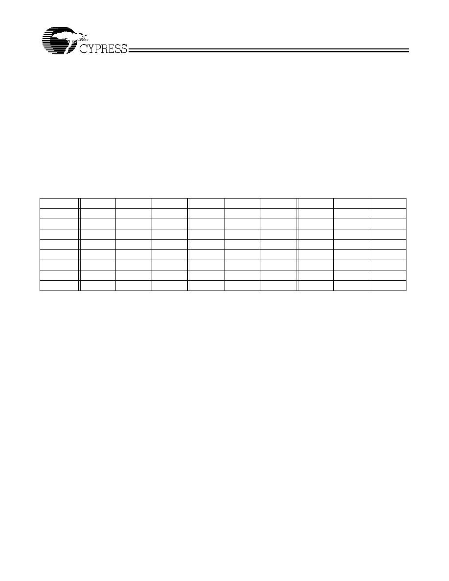
Pin Description
[2]
Pin No.
Pin Name
PWR
I/O
Type
Description
11
PECL_CLK
I
PU
PECL Clock Input.
12
PECL_CLK#
I
PD
PECL Clock Input.
9
TCLK0
I
PU
External Reference/Test Clock Input.
10
TCLK1
I
PU
External Reference/Test Clock Input.
44, 46, 48, 50
QA(3:0)
V
DDC
O
Clock Outputs. See Table 2 for frequency selections.
32, 34, 36, 38
QB(3:0)
V
DDC
O
Clock Outputs. See Table 2 for frequency selections.
16, 18, 21, 23
QC(3:0)
V
DDC
O
Clock Outputs. See Table 2 for frequency selections.
29
FB_OUT
V
DDC
O
Feedback Clock Output. Connect to FB_IN for normal operation.
The divider ratio for this output is set by FB_SEL(0:2). See Table 1.
A bypass delay capacitor at this output will control Input Reference/
Output Banks phase relationships.
25
SYNC
V
DDC
O
Synchronous Pulse Output. This output is used for system syn-
chronization. The rising edge of the output pulse is in sync with both
the rising edges of QA (0:3) and QC(0:3) output clocks regardless
of the divider ratios selected.
42, 43
SELA(1,0)
I
PU
Frequency Select Inputs. These inputs select the divider ratio at
QA(0:3) outputs. See Table 2.
40, 41
SELB(1,0)
I
PU
Frequency Select Inputs. These inputs select the divider ratio at
QB(0:3) outputs. See Table 2.
19, 20
SELC(1,0)
I
PU
Frequency Select Inputs. These inputs select the divider ratio at
QC(0:3) outputs. See Table 2.
5, 26, 27
FB_SEL(2:0)
I
PU
Feedback Select Inputs. These inputs select the divide ratio at
FB_OUT output. See Table 1.
52
VCO_SEL
I
PU
VCO Divider Select Input. When set LOW, the VCO output is di-
vided by 2. When set HIGH, the divider is bypassed. See Table 1.
31
FB_IN
I
PU
Feedback Clock Input. Connect to FB_OUT for accessing the PLL.
6
PLL_EN
I
PU
PLL Enable Input. When asserted HIGH, PLL is enabled. When
LOW, PLL is bypassed.
7
REF_SEL
I
PU
Reference Select Input. When HIGH, the PECL clock is selected.
When LOW, TCLK (0,1) is the reference clock.
8
TCLK_SEL
I
PU
TCLK Select Input. When LOW, TCLK0 is selected and when HIGH
TCLK1 is selected.
2
MR#/OE
I
PU
Master Reset/Output Enable Input. When asserted LOW, resets
all of the internal flip-flops and also disables all of the outputs. When
pulled HIGH, releases the internal flip-flops from reset and enables
all of the outputs.
14
INV_CLK
I
PU
Inverted Clock Input. When set HIGH, QC(2,3) outputs are invert-
ed. When set LOW, the inverter is bypassed.
3
SCLK
I
PU
Serial Clock Input. Clocks data at SDATA into the internal register.
4
SDATA
I
PU
Serial Data Input. Input data is clocked to the internal register to
enable/disable individual outputs. This provides flexibility in power
management.
17, 22, 28,
33,37, 45, 49
VDDC
3.3V Power Supply for Output Clock Buffers.
13
VDD
3.3V Supply for PLL
1, 15, 24, 30,
35, 39, 47, 51
VSS
Common Ground
CY29976
Document #: 38-07413 Rev. *A
Page 3 of 10
Description
The CY29976 has an integrated PLL that provides low-skew
and low-jitter clock outputs for high-performance microproces-
sors. Three independent banks of four outputs as well as an
independent PLL feedback output, FB_OUT, provide excep-
tional flexibility for possible output configurations. The PLL is
ensured stable operation given that the VCO is configured to
run between 200 MHz to 480 MHz. This allows a wide range
of output frequencies up to125 MHz.
The phase detector compares the input reference clock to the
external feedback input. For normal operation, the external
feedback input, FB_IN, is connected to the feedback output,
FB_OUT. The internal VCO is running at multiples of the input
reference clock set by FB_SEL(0:2) and VCO_SEL select in-
puts, refer to Frequency Table. The VCO frequency is then
divided down to provide the required output frequencies.
These dividers are set by SELA(0,1), SELB(0,1), SELC(0,1)
select inputs, see Table 2 below. For situations were the VCO
needs to run at relatively low frequencies and hence might not
be stable, assert VCO_SEL low to divide the VCO frequency
by 2. This will maintain the desired output relationships, but will
provide an enhanced PLL lock range.
The CY29976 is also capable of providing inverted output
clocks. When INV_CLK is asserted HIGH, QC2 and QC3 out-
put clocks are inverted. These clocks could be used as feed-
back outputs to the CY29976 or a second PLL device to gen-
erate early or late clocks for a specific design. This inversion
does not affect the output to output skew.
Table 2.
VCO_SEL
SELA1
SELA0
QA
SELB1
SELB0
QB
SELC1
SELC0
QC
0
0
0
VCO/4
0
0
VCO/4
0
0
VCO/16
0
0
1
VCO/12
0
1
VCO/12
0
1
VCO/4
0
1
0
VCO/8
1
0
VCO/8
1
0
VCO/12
0
1
1
VCO/24
1
1
VCO/20
1
1
VCO/8
1
0
0
VCO/2
0
0
VCO/2
0
0
VCO/8
1
0
1
VCO/6
0
1
VCO/6
0
1
VCO/2
1
1
0
VCO/4
1
0
VCO/4
1
0
VCO/6
1
1
1
VCO/12
1
1
VCO/10
1
1
VCO/4

CY29976
Document #: 38-07413 Rev. *A
Page 4 of 10
Z
ero Delay Buffer
When used as a zero delay buffer the CY29976 will likely be
in a nested clock tree application. For these applications the
CY29976 offers a low voltage PECL clock input as a PLL ref-
erence. This allows the user to use LVPECL as the primary
clock distribution device to take advantage of its far superior
skew performance. The CY29976 then can lock onto the
LVPECL reference and translate with near zero delay to low
skew outputs.
By using one of the outputs as a feedback to the PLL the prop-
agation delay through the device is eliminated. The PLL works
to align the output edge with the input reference edge thus
producing a near zero delay. The reference frequency affects
the static phase offset of the PLL and thus the relative delay
between the inputs and outputs. Because the static phase off-
set is a function of the reference clock the Tpd of the CY29976
is a function of the configuration used.
Glitch-Free Output Frequency Transitions
Customarily when output buffers have their internal counter's
changed "on the fly' their output clock periods will:
∑ Contain short or "runt" clock periods. These are clock cycles
in which the cycle(s) are shorter in period than either the
old or new frequency that is being transitioned to.
∑ Contain stretched clock periods. These are clock cycles in
which the cycle(s) are longer in period than either the old
or new frequency that is being transitioned to.
This device specifically includes logic to guarantee that runt
and stretched clock pulses do not occur if the device logic
levels of any or all of the following pins changed "on the fly"
while it is operating: SELA, SELB, SELC, and VCO_SEL.
CY29976
Document #: 38-07413 Rev. *A
Page 5 of 10
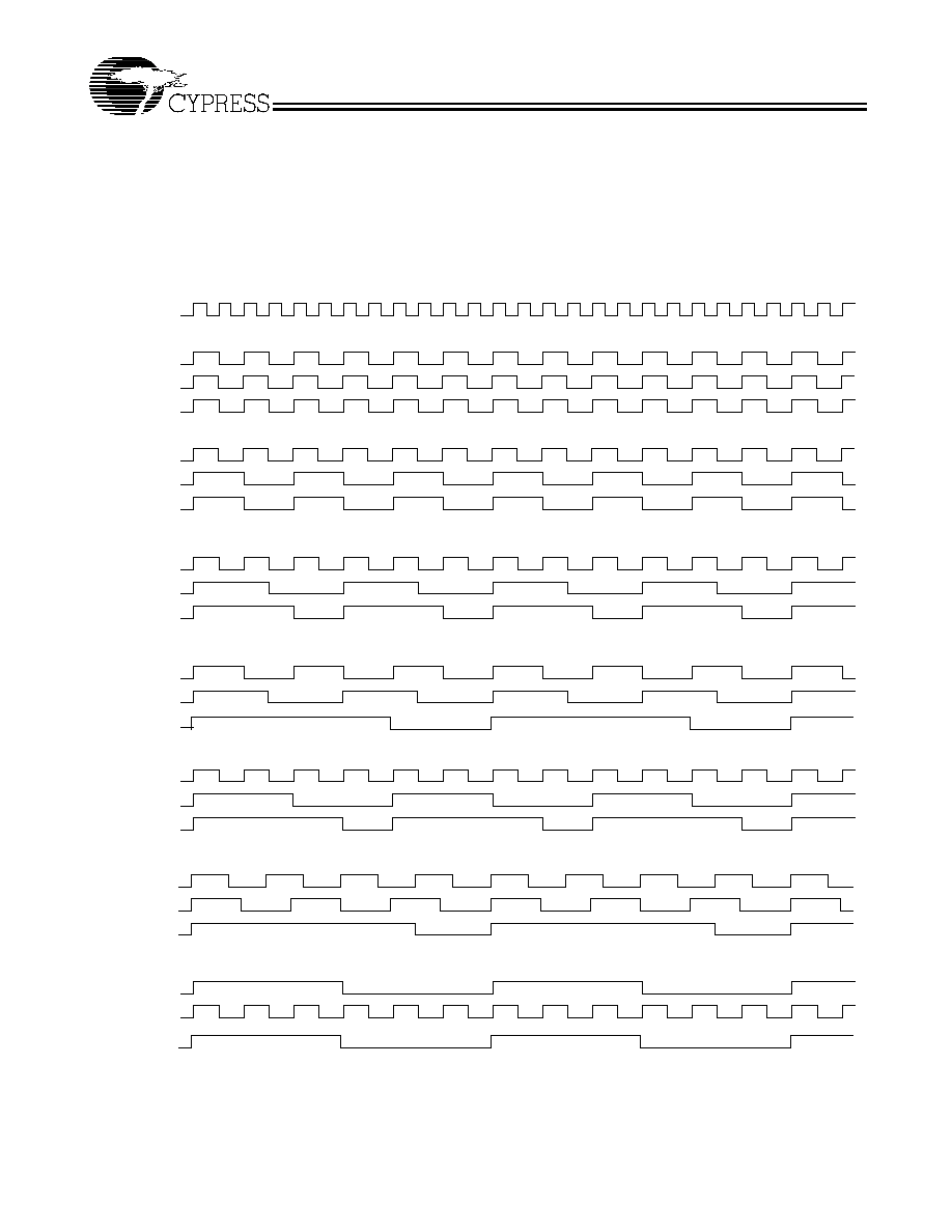
SYNC Output
In situations were output frequency relationships are not inte-
ger multiples of each other the SYNC output provides a signal
for system synchronization. The CY29976 monitors the rela-
tionship between the QA and the QC output clocks. It provides
a low going pulse, one period in duration, one period prior to
the coincident rising edges of the QA and QC outputs. The
duration and the placement of the pulse depend on the higher
of the QA and QC output frequencies. The following timing
diagram (Figure 1) illustrates various waveforms for the SYNC
output. Note that the SYNC output is defined for all possible
combinations of the QA and QC outputs even though under
some relationships the lower frequency clock could be used
as a synchronizing signal.
SYNC
QC
QA
SYNC
QC
QA
SYNC
QA
QC
SYNC
QC
QA
SYNC
QA
QC
SYNC
QC
QA
SYNC
QC
QA
VCO
1:1 Mode
2:1 Mode
3:1 Mode
3:2 Mode
4:1 Mode
4:3 Mode
6:1 Mode
Figure 1.