18-Bit Universal Bus/Driver with Three-State Outputs
CY2AVC16835
Cypress Semiconductor Corporation
∑
3901 North First Street
∑
San Jose
,
CA 95134
∑
408-943-2600
Document #: 38-07462 Rev. *A
Revised April 16, 2003
Features
∑ Less than 2.8-nS maximum input to output delay at 3.3V.
∑ Wide supply voltage range of 1.2V to 3.6 V
∑ Over voltage- tolerant inputs/outputs allow
mixed-voltage-mode data communications
∑ Output circuitry with VOITM control minimizes
over/undershoot and maximizes output drive
∑ Configurable as latch or register
∑ Extended temp range of ≠40
∞
to + 85
∞
C
∑ 2KV ESD
∑ 56-pin TSSOP package
Description
The CY2AVC16835 is a high performance, low voltage 18-bit
universal bus driver. It is operational from 1.2V to 3.6V V
DD
,
but is designed specifically for 1.5V to 3.6V V
DD
operation.
Data flow from A to Y is controlled by the output-enable (OE).
The device operates in the transparent mode when the
latch-enable (LE) input is high. The A data is latched if the
clock (CLK) input is held at a high or low logic level. If LE is
low, the A data is stored in the latch/flip-flop on the low-to-high
transition of CLK. When OE is high, the outputs are in the
high-impedance state.
To ensure the high-impedance state during power up or power
down, OE should be tied V
DD
through a pullup resistor; the
minimum value of the resistor is determined by the
current-sinking capability of the OE driving device.
The output circuitry is dynamically controlled via Variable
Output Impedance (VOI), which, during output transitions,
initially lowers the output impedance to effectively drive the
load and, subsequently, raises the impedance to reduce noise.
Figure 1 shows typical VOL vs. IOL and VOH vs IOH curves
to illustrate the output impedance and drive capability of the
circuit.
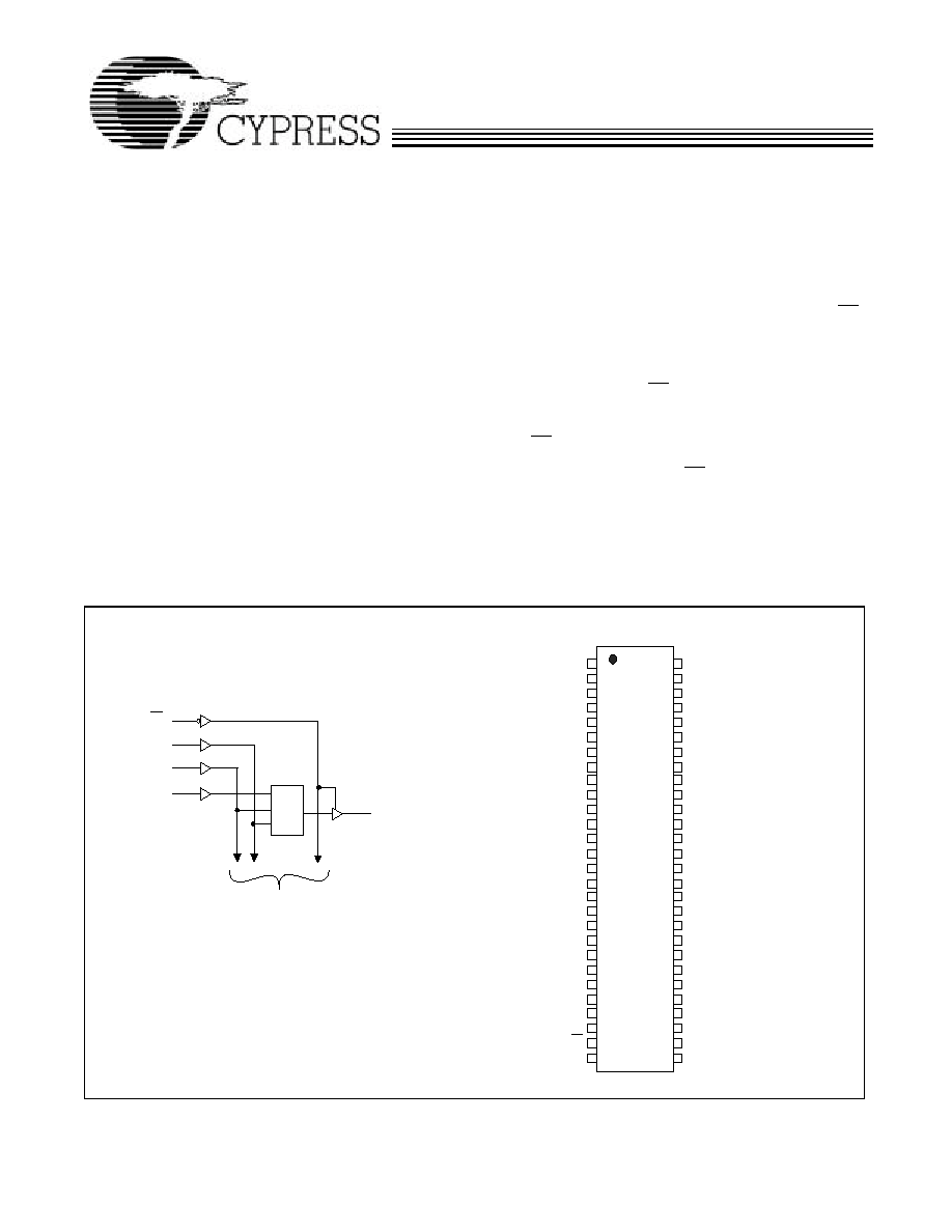
Block Diagram
Pin Configuration
To 17 Other Channels
Y1
A1
LE
CLK
OE
27
30
28
54
3
CLK
LE
D
1
2
3
4
5
6
7
8
9
10
11
12
13
14
15
16
17
18
19
20
21
22
23
24
25
26
27
28
NC
NC
Y1
V
SS
Y2
Y3
V
DD
Y4
Y5
Y6
V
SS
Y7
Y8
Y9
Y10
Y11
Y12
V
SS
Y13
Y14
Y15
V
DD
Y16
Y17
V
SS
Y18
OE
LE
56
55
54
53
52
51
50
49
48
47
46
45
44
43
42
41
40
39
38
37
36
35
34
33
32
31
30
29
V
SS
NC
A1
V
SS
A2
A3
V
DD
A4
A5
A6
V
SS
A7
A8
A9
A10
A11
A12
V
SS
A13
A14
A15
V
DD
A16
A17
V
SS
A18
CLK
V
SS
CY
2AVC1
683
5
CY2AVC16835
Document #: 38-07462 Rev. *A
Page 2 of 10
Pin Description
Pin No.
Name
Description
1,2,55
NC
No Connect
3, 5, 6, 8, 9, 10, 12,13, 14, 15,16, 17, 19,
20, 21, 23, 24, 26
Y(1:18)
Data Outputs
4, 11, 18, 25, 29, 32, 39, 46, 53, 56
V
SS
Ground
7, 22, 35, 50
V
DD
Positive Supply Voltage
27
OE
Output Enable Pin (Active LOW)
28
LE
Latch Enable (Transparent High)
30
CLK
Clock
54, 52, 51, 49, 48, 47, 45, 44, 43, 42, 41,
40, 38, 37, 36, 34, 33, 31
A (1:18)
Data Inputs
Table 1. Function Table
Inputs
Outputs
[1]
OE
LE
CLK
A
Y
H
X
X
X
Z
L
H
X
L
L
L
H
X
H
H
L
L
L
L
L
L
H
H
L
L
L/H
X
Y
Table 2. Capacitance Table
[2]
Parameter
Description
Conditions
Typ.
Max.
Unit
Cin
Input Capacitance
Vin = 0V
2.5
7
pF
Cout
Output Capacitance
Vout = 0V
6.5
9
pF
CI/O
I/O Port Capacitance
Vin = 0V
6.5
9
pF
Notes:
1.
Output level before the indicated steady_state input conditions were established, provided that CLK is high before LE goes low.
2.
As applicable to device type.
CY2AVC16835
Document #: 38-07462 Rev. *A
Page 3 of 10
Variable Output Impedance Control
Absolute Maximum Conditions
[3, 4]
Parameter
Description
Max.
Unit
V
TERM
[5]
Terminal Voltage with respect to V
SS
≠0.5 to + 4.6
V
V
TERM
[6]
Terminal Voltage with respect to V
SS
≠0.5 to V
DD
+ 0.5
V
T
STG
Storage Temperature
≠65
∞
to + 150∞C
∞C
I
OUT
DC Output Current
≠50 to + 50
mA
I
IK
Continuous Clamp Current, VI<0 or VI>V
DD
±100
mA
I
OK
Continuous Clamp Current, Vo<0
≠50
mA
I
DD
I
SS
Continuous Current through each V
DD
or V
SS
±100
mA
DC Electrical Specifications
(T
AMB
= ≠40
∞
C to +85
∞
C)
Parameter
Description
Conditions
Min.
Typ.
[7]
Max.
Unit
V
IH
High-level
input
voltage
V
DD
= 1.2V
V
DD
≠
≠
V
V
DD
= 1.4V to 1.65V
0.65 ◊ V
DD
≠
≠
V
V
DD
= 1.65V to 1.95V
0.65 V
DD
≠
≠
V
V
DD
= 2.3V to 2.7V
1.7
≠
≠
V
V
DD
= 3.0V to 3.6V
2.0
≠
≠
V
V
IL
Low-level input voltage
V
DD
= 1.2V
≠
≠
V
SS
V
V
DD
= 1.4V to 1.65V
≠
≠
0.35 V
DD
V
V
DD
= 1.65V to 1.95V
≠
≠
0.35 V
DD
V
V
DD
= 2.3V to 2.7V
≠
≠
0.7
V
V
DD
= 3.0V to 3.6V
≠
≠
0.8
V
Notes:
3.
The Voltage on any input or I/O pin cannot exceed the power pin during power-up. Power supply sequencing is NOT required.
4.
Stresses greater that those listed under Maximum Ratings may cause permanent damage to the device. This is a stress rating only and functional operation
of the device at these or any other conditions above those indicated in the operational sections of this specification is not implied. Exposure to absolute maximum
rating conditions for extended period may affect reliability.
5.
VDD terminals.
6.
All terminals except VDD.
Pull Up
0
0.5
1
1.5
2
2.5
3
3.5
-0.18
-0.16
-0.14
-0.12
-0.1
-0.08
-0.06
-0.04
-0.02
0
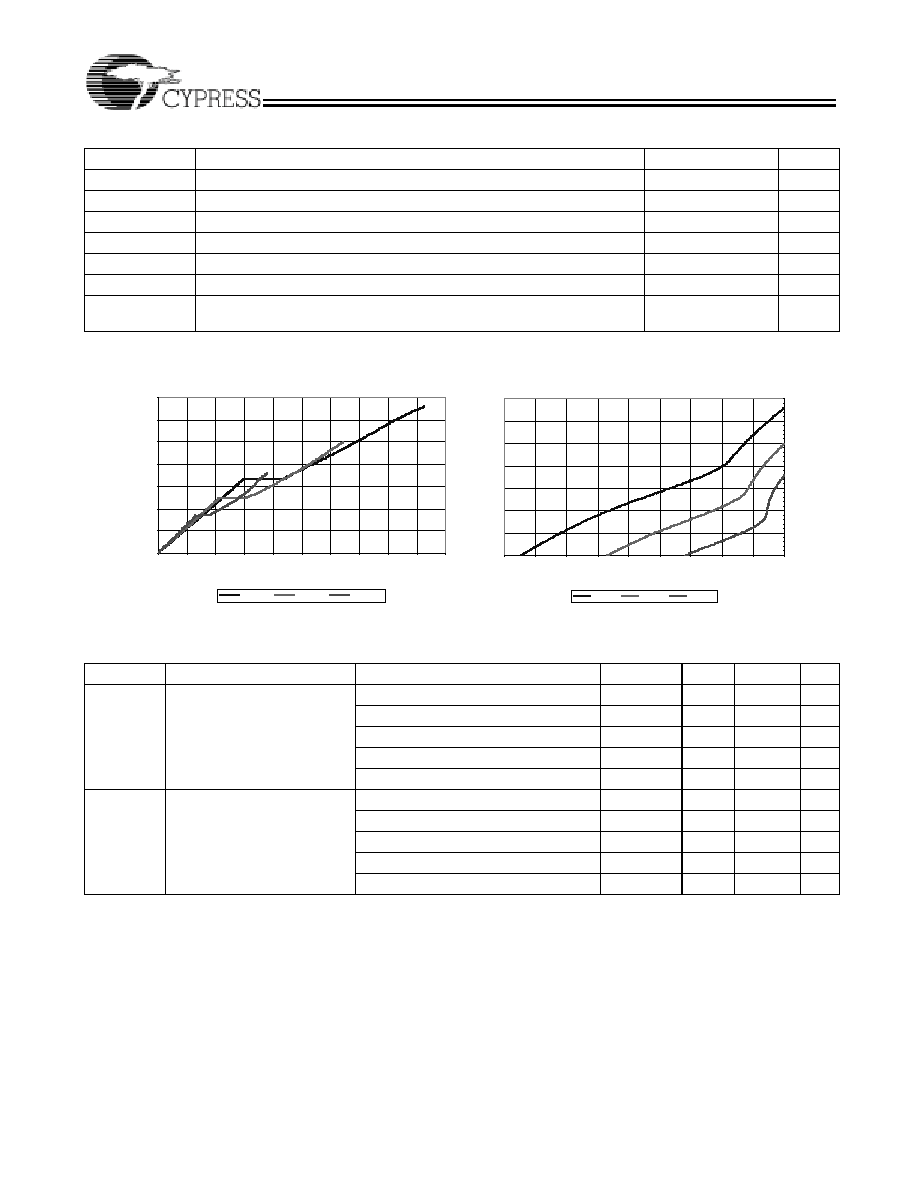
Ioh (A)
Vdd = 3.3 V
Vdd = 2.5 V
Vdd = 1.8 V
Pull Down
0
0.5
1
1.5
2
2.5
3
3.5
0
0.01
0.02
0.03
0.04
0.05
0.06
0.07
0.08
0.09
0.1
Iol (A)
Vdd = 3.3 V
Vdd = 2.5 V
Vdd = 1.8 V
Figure 1. Output Voltage vs. Output Current (TA = 25∞C)
CY2AVC16835
Document #: 38-07462 Rev. *A
Page 4 of 10
V
OH
[8]
High-level output voltage
V
DD
= 1.4V to 3.6V
I
O
= ≠100 µA
V
DD
-0.20
≠
≠
V
V
DD
= 1.4V
I
O
= ≠2 µA
1.05
≠
≠
V
V
DD
= 1.65V
I
O
= ≠4 mA
1.2
≠
≠
V
V
DD
= 2.3V
I
O
= ≠8 mA
1.75
≠
≠
V
V
DD
= 3.0V
I
O
= ≠12 mA
2.3
≠
≠
V
V
DD
= 1.4V to 3.6V
I
O
= 100 µA
≠
≠
0.20
V
V
OL
[8]
Low-level output voltage
V
DD
= 1.4V
I
O
= 2 mA
≠
≠
0.40
V
V
DD
= 1.65V
I
O
= 4 mA
≠
≠
0.45
V
V
DD
= 2.3V
I
O
= 8 mA
≠
≠
0.55
V
V
DD
= 3.0V
I
O
= 12 mA
≠
≠
0.70
V
I
I
Input leakage current per pin
V
DD
= 1.65V to 3.6V Vin = V
DD
or V
SS
≠
≠
±2.5
µA
I
OFF
Power off leakage current
V
I
or V
O
= 3.6V
V
DD
= 0V
≠
≠
±10
µA
I
DD
Quiescent supply Current
V
DD
= 3.6V
I
O
= 0
≠
≠
40
µA
I
OZ
Three-state output OFF-state
current
V
DD
= 3.6V
V
O
= V
DD
or V
Ss
≠
≠
±10
µA
DC Electrical Specifications
(T
AMB
= ≠40
∞
C to +85
∞
C) (continued)
Parameter
Description
Conditions
Min.
Typ.
[7]
Max.
Unit
AC Electrical Specifications
Parameters
V
DD
= 1.2V
V
DD
=1.5V
+ 0.1V
V
DD
=1.8V
+ 0.15V
V
DD
=2.5V
+ 0.2V
V
DD
=3.3V
+ 0.3V
Unit
Min.
Max.
Min.
Max.
Min.
Max.
Min.
Max.
Min.
Max.
F
clock
Clock Frequency
≠
≠
≠
≠
≠
150
≠
150
≠
150
MHz
tw
Pulse
Duration
LE high
≠
≠
≠
≠
3.3
≠
3.3
≠
3.3
≠
ns
CLK High or Low
≠
≠
≠
≠
3.3
≠
3.3
3.3
1.0
≠
ns
tsu
Set-up
Time
Data Before CLK
HIGH
1.0
≠
0.9
≠
0.7
≠
0.7
≠
0.7
≠
ns
Data
Before LE
LOW
CLK High
1.7
≠
1.6
≠
1.2
≠
0.8
≠
0.8
≠
≠
CLK Low
2.0
≠
0.9
≠
0.7
≠
0.5
≠
0.5
≠
≠
th
Hold time
Data after CLK HIGH
1.5
≠
1.3
≠
1.0
≠
0.9
≠
1.3
≠
ns
Data After CLK High
3.2
≠
2.4
≠
2.0
≠
1.7
≠
1.6
≠
ns
LE LOW
Or Low
2.8
≠
2.1
≠
1.7
≠
1.5
1.4
≠
≠
From
To
Typ.
≠
≠
≠
≠
≠
≠
≠
≠
≠
t
pd
An
Yn
4.5
1.2
6.2
1.3
5.5
1.0
3.1
0.9
2.5
ns
LE
6.2
1.6
9.4
1.3
7.2
1.1
4.7
0.9
3.8
CLK
5.2
1.6
7.8
1.5
6
1
3.7
0.8
3.1
t
en
OE
Yn
7.1
2.4
10.2
2.2
8.8
1.5
6.7
1.2
6.2
ns
t
dis
OE
Yn
6.9
2.2
10.3
2
8.4
1.2
5.3
1.1
5.3
ns
Notes:
7.
All typical values are measured at T
AMB
= 25∞C.
8.
V
IN
= V
IL
or V
IH
.
CY2AVC16835
Document #: 38-07462 Rev. *A
Page 5 of 10
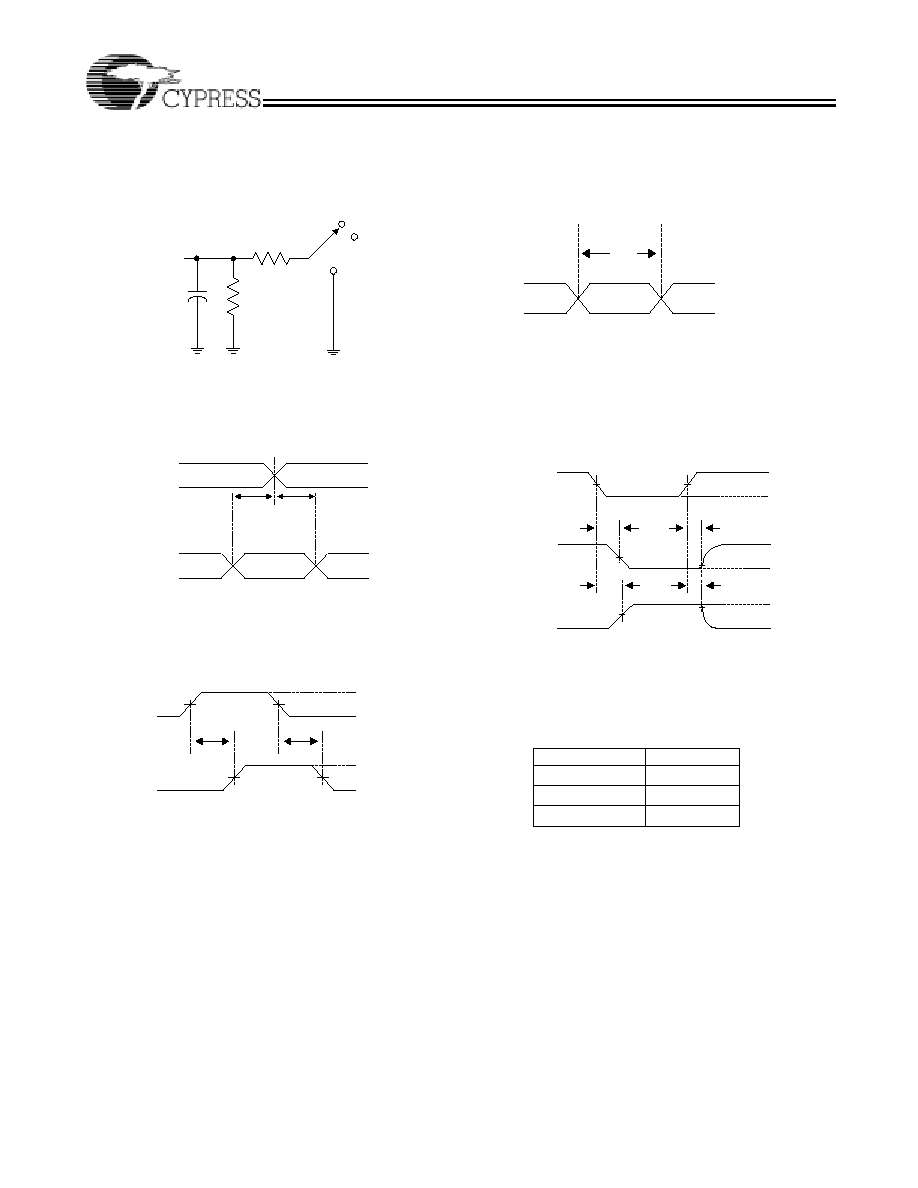
Parameter Measurement
V
DD
= 1.2V and 1.5V ± 0.1V
Timing Diagrams
Notes:
9.
CL includes probe and jig capacitance.
10. Waveform 1 is for an output with internal conditions such that the output is low except when disabled by the output control.
11. Waveform 2 is for an output with internal conditions such that the output is high except when disabled by the output control.
12. All input pulses are supplied by generators having the following characteristics: PRR
10MHz, Z0 = 50
, t
R
2ns, t
F
2 ns.
13. The outputs are measured one at a time with on transition per measurement.
14. t
PLZ
snf t
PHZ
are the same as t
DIS
.
15. t
PZl
and t
PZH
are the same as t
en
.
16. t
PLH
and t
PHL
are the same as t
PD
.
Test S1
tPLH/tPHL Open
tPLZ/tPZL
2 x VDD
tPHZ/tPZH
V
SS
From Output
Under Test
CL = 15 pF
2 k ohm
V
SS
Open
2x V
DD
Load Circuit
2 k ohm
S1
t
su
t
h
V
DD
/2
V
DD
0 V
0 V
Timing Input
Data Input
Voltage Waveforms
Setup and Hold Times
V
DD
/2
V
DD
/2
V
DD
V
DD
/2
t
PLH
t
PHL
V
DD
V
OH
V
OL
0 V
Input
Output
Voltage Waveforms
Propagation Delay Times
V
DD
/2
V
DD
/2
V
DD
/2
V
DD
/2
V
DD
0 V
Input
t
w
Voltage Waveforms
Pulse Duration
V
DD
/2
Output
Control
(low-level
enabling)
Output
Waveform 1
S1 at 2 x VDD
Output
Waveform 2
S1 at GND
V
D
D
t
PLZ
t
PHZ
t
PZH
t
PZL
V
DD
/2
0 V
0 V
V
OL
+ 0.1 V
V
OH
- 0.1 V
V
OL
V
OH
Voltage Waveforms
Enable and Disable Times
V
DD
/2
V
DD
/2
V
DD
/2
V
D
D
Waveform 1
Waveform 2
Waveform 3
Waveform 4
Waveform 5
Figure 2. Load Circuit and Voltage Waveforms for V
DD
= 1.2V and 1.5V ± 0.1V
[9,10,11,12,13,14,15,16]