1:10 Clock Fanout Buffer with Output Enable
COMLINKTM SERIES
CY2CC1910
Cypress Semiconductor Corporation
∑
3901 North First Street
∑
San Jose
∑
CA 95134
∑
408-943-2600
Document #: 38-07347 Rev. *B
Revised December 26, 2002
Features
∑ Low-voltage operation
∑ Full-range support:
-- 3.3V
-- 2.5V
-- 1.8V
∑ 1:10 fanout
∑ Drives either a 50-Ohm or 75-Ohm load
∑ Over voltage tolerant input hot swappable
∑ Low-input capacitance
∑ Low-output skew
∑ Low-propagation delay
∑ Typical (tpd < 4 ns)
∑ High-speed operation:
-- 100 MHz@1.8V
-- 200 MHz@2.5V/3.3V
∑ Industrial versions available
∑ Available packages include: SOIC, SSOP
Description
The Cypress series of network circuits are produced using
advanced 0.35-micron CMOS technology, achieving the
industries fastest logic and buffers.
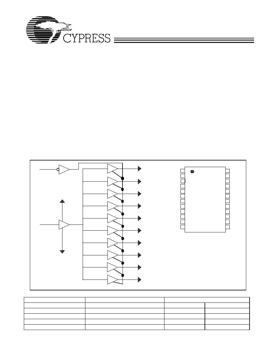
The Cypress CY2CC1910 fanout buffer features one input and
ten outputs. Ideal for conversion from/to 3.3V/2.5V/1.8V.
Designed for data communications clock management appli-
cations, the large fanout from a single input reduces loading
on the input clock.
Cypress employs unique AVCMOS-type outputs VOITM
(Variable Output Impedance) that dynamically adjust for
variable impedance matching and eliminate the need for
series damping resistors; they also reduce noise overall.
Pin Description
Pin Number
Pin Name
Pin Description
1, 7, 8, 12, 13, 17, 20, 24
G
ND
Ground
Power
3,10,15,22
V
DD
Power Supply
Power
5
OE#
Output Enable
LVTTL/LVCMOS
6
IN
Input
LVTTL/LVCMOS
2, 4, 9, 11, 14, 16, 18, 19, 21, 23 Q10, Q9, Q8, Q7, Q6, Q5, Q4, Q3, Q2, Q1 Output
AVCMOS
1
2
3
4
5
6
7
8
9
10
11
12
24
23
22
21
20
19
18
17
16
15
14
13
24 pin SOIC/SSOP
C
Y
2CC
1910
GND
Q1
VDD
Q2
GND
Q3
Q4
GND
Q5
VDD
Q6
GND
GND
Q10
Q9
OE#
IN
GND
GND
Q8
VDD
Q7
GND
VDD
1 6
1 1
1 4
1 8
2 3
1 9
2 1
9
4
2
6
OUTPUT
(AVCMOS)
OE#
5
IN
Q 5
Q 7
Q 6
Q 4
Q 1
Q 3
Q 2
Q 8
Q 9
Q 1 0
G N D
V D D
1 ,1 2 ,1 3
1 7 ,2 4
3 ,1 0
1 5 ,2 2
AVCMOS
AVCMOS
Block Diagram
Pin Configuration
COMLINKTM SERIES
CY2CC1910
Document #: 38-07347 Rev. *B
Page 2 of 8
Maximum Ratings
[1,2]
Storage Temperature: ................................≠65
∞
C to + 150
∞
C
Ambient Temperature:................................... ≠40
∞
C to +85
∞
C
Supply Voltage to Ground Potential
V
CC
.................................................................. ≠0.5V to 4.6V
Input ................................................................. ≠0.5V to 5.8V
Supply Voltage to Ground Potential
(Outputs only) ........................................... ≠0.5V to V
DD
+ 1V
DC Output Voltage.................................... ≠0.5V to V
DD
+ 1V
Power Dissipation........................................................ 0.75W
Variable Output Impedance Control (VOITM)
DC Electrical Characteristics
@ 3.3V (see Figure 2)
Parameter
Description
Conditions
Min.
Typ.
Max.
Unit
V
OH
Output High Voltage
V
DD
= Min.,V
IN
= V
IH
or V
IL
I
OH
= ≠12 mA
2.3
3.3
V
V
OL
Output Low Voltage
V
DD
= Min.,V
IN
= V
IH
or V
IL
I
OL
= 12 mA
0.2
0.5
V
V
IH
Input High Voltage
Guaranteed Logic High Level
2
5.8
V
V
IL
Input Low Voltage
Guaranteed Logic Low Level
0.8
V
I
IH
Input High Current
V
DD
= Max.
V
IN
= 2.7V
1
uA
I
IL
Input Low Current
V
DD
= Max.
V
IN
= 0.5V
≠1
uA
I
I
Input High Current
V
DD
= Max.,V
IN
= V
DD
(Max.)
20
uA
V
IK
Clamp Diode Voltage
V
DD
= Min., I
IN
= ≠18 mA
≠0.7
≠1.2
V
I
OK
Continuous Clamp Current
V
DD
= Max.,V
OUT
= GND
≠50
mA
O
OFF
Power-down Disable
V
DD
= GND,V
OUT
= < 4.5V
100
uA
V
H
Input Hysteresis
80
mV
DC Electrical Characteristics
@ 2.5V (see Figure 2)
Parameter
Description
Conditions
Min.
Typ.
Max.
Unit
V
OH
Output High Voltage
V
DD
= Min.,V
IN
= V
IH
or V
IL
I
OH
= ≠7 mA
1.8
V
V
DD
= Min.,V
IN
= V
IH
or V
IL
I
OH
= 12 mA
1.6
V
V
OL
Output Low Voltage
Guaranteed Logic High Level
I
OL
= 12 mA
0.65
V
V
IH
Input High Voltage
Guaranteed Logic Low Level
1.6
5.0
V
V
IL
Input Low Voltage
V
DD
= Max.
0.8
V
I
IH
Input High Current
V
DD
= Max.
V
IN
= 2.4V
1
uA
I
IL
Input Low Current
V
DD
= Max.,V
IN
= V
DD
(Max.)
V
IN
= 0.5V
≠1
uA
I
I
Input High Current
V
DD
= Min., I
IN
= ≠18 mA
20
uA
V
IK
Clamp Diode Voltage
V
DD
= Max.,V
OUT
= GND
≠0.7
≠1.2
V
I
OK
Continuous Clamp Current
V
DD
= GND, V
OUT
= < 4.5V
≠50
mA
O
OFF
Power-down Disable
V
DD
= Min.,V
IN
= V
IH
or V
IL
100
uA
V
H
Input Hysteresis
80
mV
Note:
1.
Multiple Supplies: The Voltage on any input or I/O pin cannot exceed the power pin during power-up. Power supply sequencing is NOT required.
2.
Stresses greater than those listed under absolute maximum ratings may cause permanent damage to the device. This is intended to be a stress rating only
and functional operation of the device at these or any other conditions above those indicated in the operation sections of this specification is not implied.
Exposure to absolute maximum rating conditions for extended periods may affect reliability.
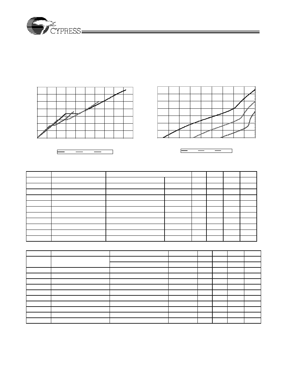
Pull Down
0
0.5
1
1.5
2
2.5
3
3.5
0
0.01
0.02
0.03
0.04
0.05
0.06
0.07
0.08
0.09
0.1
Iol (A)
Vdd = 3.3 V
Vdd = 2.5 V
Vdd = 1.8 V
Pull Up
0
0.5
1
1.5
2
2.5
3
3.5
-0.18
-0.16
-0.14
-0.12
-0.1
-0.08
-0.06
-0.04
-0.02
0
Ioh (A)
Vdd = 3.3 V
Vdd = 2.5 V
Vdd = 1.8 V
Figure 1. Output Voltage vs. Output Current (T
A
= 25∞C)
COMLINKTM SERIES
CY2CC1910
Document #: 38-07347 Rev. *B
Page 3 of 8
DC Electrical Characteristics
@ 1.8V (see Figure 6)
Parameter
Description
Test Condition
[3]
Min.
Max.
Unit
V
DD
Supply Voltage
1.71
1.89
V
V
IH
Input High Voltage
0.65V
DD
[1.1]
4.3
V
V
IL
Input Low Voltage
≠0.3
0.35V
DD
[0.6]
V
V
OH
Output High Voltage
I
OH
= ≠2 mA
V
DD
≠ 0.45[1.2]
V
V
OL
Output Low Voltage
I
OH
= 2 mA
0.45
V
Capacitance
Parameter
Description
Test Conditions
Typ.
Max.
Unit
C
IN
Input Capacitance
V
IN
= 0V
2.5
pF
C
OUT
Output Capacitance
V
OUT
= 0V
6.5
pF
Power Supply Characteristics
(see Figure 2)
Parameter
Description
Test Conditions
Min.
Typ.
Max.
Unit
I
CC
Delta I
CC
Quiescent Power
Supply Current
(I
DD
@V
DD
= Max. and V
IN
= V
DD
) ≠ (I
DD
@V
DD
= Max. and V
IN
= V
DD
≠ 0.6V)
50
uA
I
CCD
Dynamic Power Supply Current V
DD
= Max.
Input toggling 50% Duty Cycle, Outputs Open
0.63
mA/
MHz
I
C
Total Power Supply Current
V
DD
= Max.
Input toggling 50% Duty Cycle, Outputs Open
fL = 40 MHZ
25
mA
High-frequency Parametrics
Parameter
Description
Test Conditions
Min. Typ. Max. Unit
D
J
Jitter, deterministic
50% duty cycle tW(50≠50)
The "point to point load circuit"
| Output Jitter ≠ Input Jitter |
See Figure 4
20
ps
F
max
3.3V
Maximum frequency
V
DD
= 3.3V
50% duty cycle tW(50≠50)
Standard Load Circuit.
See Figure 2
160
MHz
50% duty cycle tW(50≠50)
The "point to point load circuit"
See Figure 4
200
F
max
2.5V
Maximum frequency
V
DD
= 2.5V
The "point to point load circuit"
V
IN
= 2.4V/0.0V
V
OUT
= 1.7V/0.7V
See Figure 4
200
MHz
F
max
1.8V
Maximum frequency
V
DD
= 1.8V
The "6-pF load circuit"
V
IN
= 1.7V/0.0V
V
OUT
= 1.2V/0.4V
See Figure 6
100
MHz
F
max(20)
Maximum frequency
V
DD
= 3.3V
20% duty cycle tW(20≠80)
The "point to point load circuit"
V
IN
= 3.0V/0.0V
V
OUT
= 2.3V/0.4V
See Figure 4
250
MHz
t
W
3.3V
Minimum pulse
V
DD
= 3.3V
The "point to point load circuit"
V
IN
= 3.0V/0.0V F = 100 MHz
V
OUT
= 2.0V/0.8V
See Figure 4
1
ns
t
W
2.5V
Minimum pulse
V
DD
= 2.5V
The "point to point load circuit"
V
IN
= 2.4V/0.0V F = 100 MHz
V
OUT
= 1.7V/0.7V
See Figure 4
1
tW
1.8V
Minimum pulse
V
DD
= 1.8V
The "6-pF load circuit"
V
IN
= 1.7V/0.0V
V
OUT
= 1.2V/0.4V
See Figure 6
1
Note:
3.
Test Load conditions: 500 ohm to ground with approximately 6-pF total loading and 200-MHz maximum frequency.
COMLINKTM SERIES
CY2CC1910
Document #: 38-07347 Rev. *B
Page 4 of 8
Parameter Measurement Information:
V
DD
@ 3.3V≠2.5V
Notes:
4.
C
L
includes probe and jig capacitance.
5.
All input pulses are supplied by generators having the following characteristics: PRR < 100 MHz, Z
0
= 50
, t
R
< 2.5 nS, t
F
< 2.5 nS.
6.
The outputs are measured one at a time with one transition per measurement.
7.
T
PLH
and T
PHL
are the same as t
pd
.
AC Switching Characteristics
@ 3.3V V
DD
= 3.3V ± 5%, Temperature = ≠40
∞
C to +85
∞
C
Parameter
Description
Min.
Typ.
Max.
Unit
t
PLH
Propagation Delay ≠ Low to High
Figure 3
1.5
2.7
3.5
nS
t
PHL
Propagation Delay ≠ High to Low
1.5
2.7
3.5
nS
t
R
Output Rise Time
0.8
V/nS
t
F
Output Fall Time
0.8
V/nS
t
SK(0)
Output Skew: Skew between outputs of the same package (in phase)
Figure 10
0.2
nS
t
SK(p)
Pulse Skew: Skew between opposite transitions of the same output (t
PHL
≠ t
PLH
).
Figure 9
0.2
nS
t
SK(t)
Package Skew: Skew between outputs of different packages at the same
power supply Voltage, temperature and package type.
Figure 11
0.4
nS
AC Switching Characteristics
@ 2.5V V
DD
= 2.5V ± 5%, Temperature = ≠40
∞
C to +85
∞
C
Parameter Description
Min.
Typ.
Max.
Unit
t
PLH
Propagation Delay ≠ Low to High
Figure 3
1.5
2.7
3.5
nS
t
PHL
Propagation Delay ≠ High to Low
1.5
2.7
3.5
nS
t
R
Output Rise Time
0.8
V/nS
t
F
Output Fall Time
0.8
V/nS
t
SK(0)
Output Skew: Skew between outputs of the same package (in phase)
Figure 10
0.2
nS
t
SK(p)
Pulse Skew: Skew between opposite transitions of the same output (t
PHL
≠ t
PLH
).
Figure 9
0.2
nS
t
SK(t)
Package Skew: Skew between outputs of different packages at the
same power supply Voltage, temperature and package type.
Figure 11
0.4
nS
AC Switching Characteristics
@ 1.8V V
DD
= 1.8V ± 5%, Temperature = ≠40
∞
C to +85
∞
C
Parameter
Description
Min.
Typ.
Max.
Unit
t
PLH
Propagation Delay ≠ Low to High
Figure 7
1.5
2.7
3.5
nS
t
PHL
Propagation Delay ≠ High to Low
1.5
2.7
3.5
nS
t
R
Output Rise Time 20≠80%
0.2
1.5
nS
t
F
Output Fall Time 20≠80%
0.2
1.5
nS
t
SK(0)
Output Skew: Skew between outputs of the same package (in phase)
Figure 10
0.2
nS
t
SK(p)
Pulse Skew: Skew between opposite transitions of the same output (t
PHL
≠ t
PLH
).
Figure 9
0.2
nS
t
SK(t)
Package Skew: Skew between outputs of different packages at the same
power supply Voltage, temperature and package type.
Figure 11
0.4
nS
From Output
Under Test
C
L
= 50 pF
500 ohm
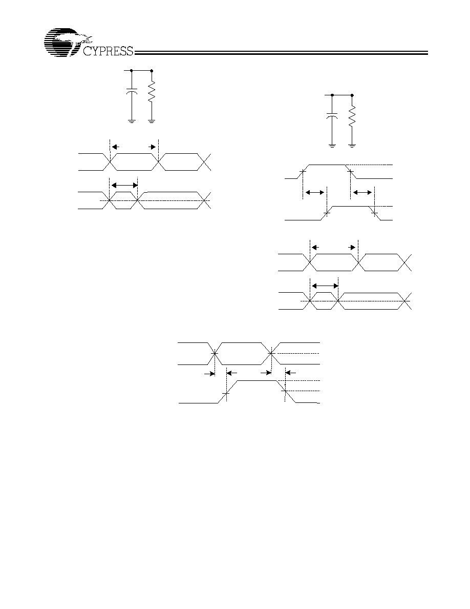
Figure 2. Load Circuit
[4,5,6]
VDD/2
t
PLH
t
PHL
V
OH
V
OL
0 V
Input
Output
VDD/2
VDD/2
VDD/2
0.8VDD
Figure 3. Voltage Waveforms Propagation Delay Times
[7]
COMLINKTM SERIES
CY2CC1910
Document #: 38-07347 Rev. *B
Page 5 of 8
Parameter Measurement Information: V
DD
@
1.8V
From Output
Under Test
C
L
= 3 pF
500 ohm
Figure 4. Point to Point Load Circuit
[4,5,6]
0 V
Input
t
w(20-80)
0.8VDD
0 V
VDD/2
Input
t
w(50-50)
VDD/2
VDD/2
0.8VDD
Figure 5. Voltage Waveforms≠Pulse Duration
[5]
From Output
Under Test
C
L
= 6 pF
500 ohm
Figure 6. Load Circuit
[4,5,6]
0.9V
t
PLH
t
PHL
1.8V
V
OH
V
OL
0 V
Input
Output
0.9V
0.9V
0.9V
Figure 7. Voltage Waveforms Propagation Delay Times
[7]
0 V
Input
t
w(20-80)
1.8V
0 V
0.9V
Input
t
w(50-50)
0.9V
0.9V
1.8V
Figure 8. Voltage Waveforms≠Pulse Duration
[5]
INPUT
OUTPUT
t
PLH
t
PHL
tsk
(P)
=
l
t
PHL
- t
PLH
l
3V
1.5V
0V
VOH
1.5V
VOL
Figure 9. Pulse Skew - tsk
(p)