High-drive Dual 2-Channel LVDS Repeater/Mux
ComLinkTM Series
CY2LL8423
Cypress Semiconductor Corporation
∑
3901 North First Street
∑
San Jose
,
CA 95134
∑
408-943-2600
Document #: 38-07065 Rev. *B
Revised January 30, 2003
Features
∑ ANSI TIA/EIA-644-1995-compliant
∑ Designed for data rates to > 650 Mbps = (325 MHz)
∑ Single 2 ◊ 2 with high-drive output drivers
-- Low-voltage Differential Signaling with output
voltages of ± 350 mV into 50-ohm load version (Bus
LVDS)
∑ Single 3.3V supply
∑ Accepts ±350-mV differential inputs
∑ Output drivers are high impedance when disabled or
when VDD <1.5V
∑ 28-pin SSOP/TSSOP packages
∑ Industrial version available
Description
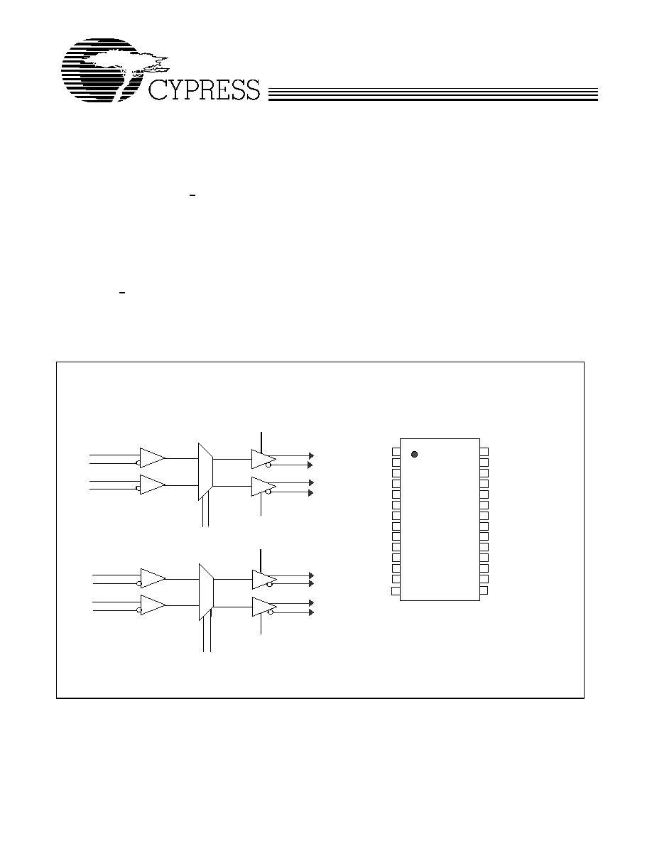
The Cypress CY2LL8423 are differential line drivers and
receivers that utilize low-voltage differential signaling (LVDS)
to achieve signaling rates of 650 Mbps. The receiver outputs
can be switched to either or both drivers through the multi-
plexer control signals S2/S3. This provides flexibility in appli-
cation for either a splitter or router configuration with a single
device.
The Cypress CY2LL8423 are configured as a dual 2-channel
repeater/Mux. The LVDS standard provides a minimum differ-
ential output voltage of 247 mV into a 50-ohm load and receipt
of as little as 100-mV signals with up to 1V of DC offset
between transmitter and receiver.
A doubly-terminated Bus LVDS line enables multipoint config-
urations.
Designed for both point-to-point based-B and multipoint data
transmission over controlled impedance lines.
Block Diagram
Pin Configuration
1 Y
1 Z
2 Y
2 Z
2 7
2 6
2 3
2 4
1 A
1 B
2 A
2 B
2
1
6
7
1 D E
2 D E
3
5
S0 S1
3 Y
3 Z
4 Y
4 Z
2 0
1 9
1 7
1 6
3 A
3 B
4 A
4 B
8
9
1 3
1 4
1 0
1 2
S2 S3
3 D E
4 D E
1 1
1 8
2 5
4
VDD
1Y
1Z
2DE
2Z
2Y
3Z
3Y
4DE
4Z
4Y
GND
GND
VDD
28 pin TSSOP/SSOP
CY
2LL
8
423
1
2
3
4
5
6
7
8
9
10
11
12
13
14
20
28
27
26
25
24
23
22
21
15
16
17
18
19
1B
1A
S0
1DE
S1
2A
2B
3B
3A
S2
3DE
S3
4A
4B
ComLinkTM Series
CY2LL8423
Document #: 38-07065 Rev. *B
Page 2 of 9
Pin Description
Pin Number
Pin Name
Description
15, 22
GND
Ground
2, 1
1A, 1B
Differential Input Channel 1
3
S0
Function Select Channel 1&2
4
1DE
Data Enable Channel 1
5
S1
Function Select Channel 1& 2
6, 7
2A, 2B
Differential Input Channel 2
21, 28
VDD
Power Supply
8, 9
3A, 3B
Differential Input Channel 3
10
S2
Function Select Channel 3 & 4
11
3DE
Data Enable Channel 3
12
S3
Function Select Channel 3 & 4
13, 14
4A, 4B
Differential Input Channel 4
17, 16
4Y, 4Z
Differential Output Channel 4
18
4DE
Data Enable Channel 4
20, 19
3Y, 3Z
Differential Output Channel 3
23, 24
2Y, 2Z
Differential Output Channel 2
25
2DE
Data Enable Channel 2
27, 26
1Y, 1Z
Differential Output Channel 1
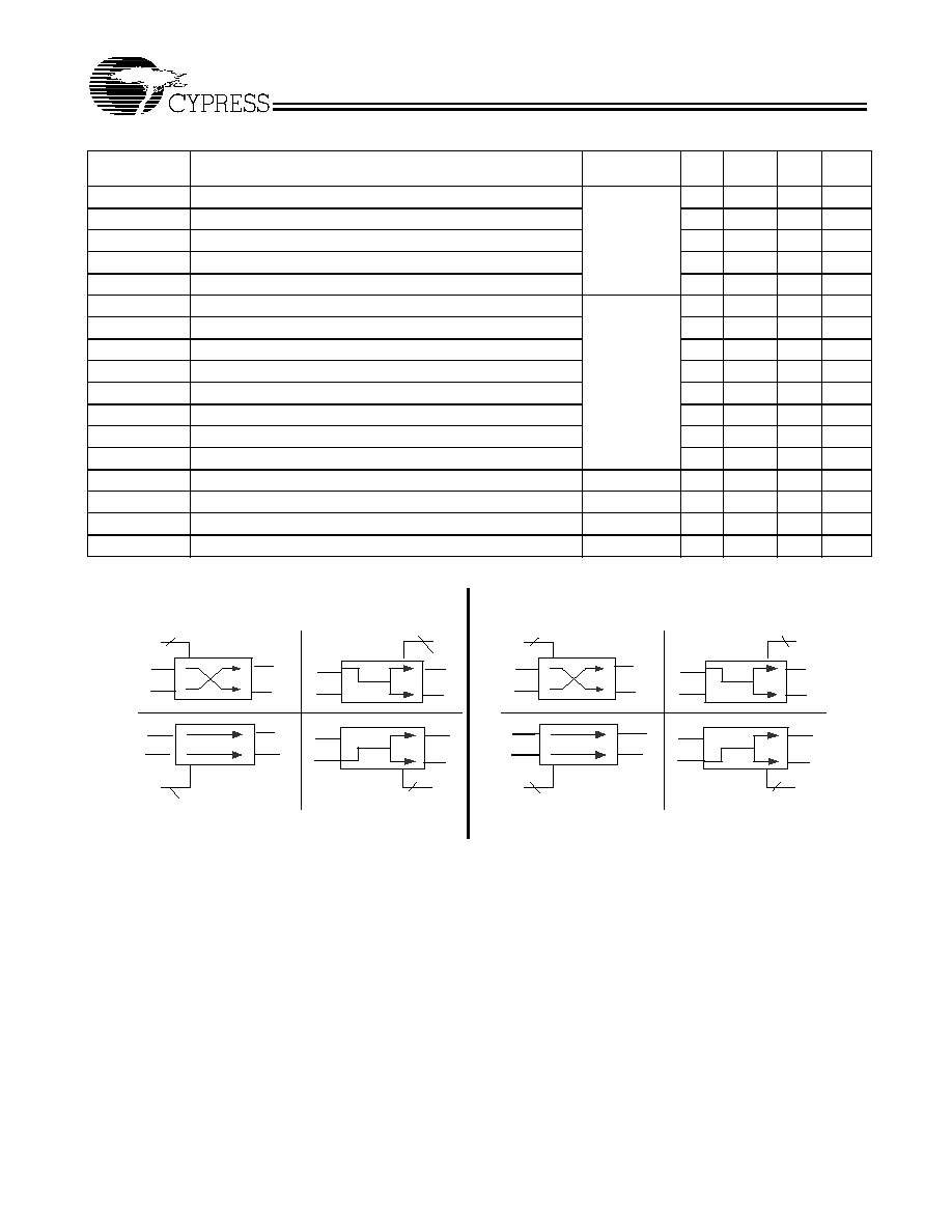
Table 1. Mux Function Table
Input
Output
Function
S0
S1
1Y/1Z
2Y/2Z
0
0
1A/1B
1A/1B
Splitter A
1
0
2A/2B
2A/2B
Splitter B
0
1
1A/1B
2A/2B
Pass Thru Router
1
1
2A/2B
1A/1B
Cross Point Router
S2
S3
3Y/3Z
4Y/4Z
0
0
3A/3B
3A/3B
Splitter A
1
0
4A/4B
4A/4B
Splitter B
0
1
3A/3B
4A/4B
Pass Thru Router
1
1
4A/4B
3A/3B
Cross Point Router
Table 2. Absolute Maximum Rating Over Operating Free-Air Temperature
[1]
Supply Voltage Range, V
DD
(1)
≠0.5V to 4V
Voltage Range (DE,S0,S1)
≠0.5V to 6.0V
Input Voltage Range, V
IN
(A or B)
≠0.5V to V
DD
+ 0.5V
ESD (All pins)
Class 3, A: 2KV, B: 500V
Storage Temperature Range
≠65∞C to 150∞C
Note:
1.
Stresses greater than those listed under absolute maximum ratings may cause permanent damage to the device. This is intended to be a stress rating only
and functional operation of the device at these or any other conditions above those indicated in the operation sections of this specification is not implied.
Exposure to absolute maximum rating conditions for extended periods may affect reliability.
ComLinkTM Series
CY2LL8423
Document #: 38-07065 Rev. *B
Page 3 of 9
Table 3. Recommended Operating Conditions
[2]
Parameter
Description
Min.
Typ.
Max.
Unit
V
DD
Supply Voltage
3
3.3
3.6
V
V
IH
High Level Input Voltage
(S0,S1,1DE,2DE)
(S2,S3,3DE,4DE)
2
V
IL
Low Level Input Voltage
(S0,S1,1DE,2DE)
(S2,S3,3DE,4DE)
0.8
V
ID
Magnitude of Differential Input Voltage
0.1
0.6
V
IC
Common Mode Input Voltage
V
ID
/2
2.4 ≠ (V
ID
/2)
T
A
Operating Free Air Temperature
Industrial
≠40
85
∞C
Commercial
0
70
Table 4. Receiver Electrical Characteristics Over Recommended Operating Conditions
Parameter
Description
Condition
Min.
Typ.
Max.
Unit
V
ITH+
Positive-going Differential Input Voltage Threshold
V
CM
= 1.2V
100
mV
V
ITH-
Negative-going Differential Input Voltage Threshold
V
CM
= 1.2V
≠100
mV
I
I
Input Current (A Inputs) [FAIL SAFE]
V
I
= 0V
≠0.5
≠10
µ
A
V
I
= 2.4V
≠10
µ
A
I
I
Input Current (B Inputs) [FAIL SAFE]
V
I
= 0.8V
0.5
10
µ
A
V
I
= 2.4V
10
µ
A
I
I
(Off)
Power Off Current (A or B Inputs)
V
DD
= 0V
0.1
10
µ
A
Table 5. Receiver Electrical Characteristics Over Recommended Operating Conditions
Parameter
Description
Condition
Min.
Typ.
Max.
Unit
V
OD
Differential Output Voltage Swing
RL = 50 Ohm
See Figure 3
247
340
454
mV
~V
OD
Change in Differential Output Voltage
Swing between Logic States
≠50
50
mV
V
OC
(SS)
Steady State Common-mode Output Voltage
See Figure 4
1.125
1.375
V
~V
OC
(SS)
Change in Steady State Common-mode
Output between Logic States
≠50
3
50
mV
V
OC
(PP)
Peak-to-Peak Common-mode Output Voltage
150
mV
I
CC
Supply Current
No load
20
28
mA
RL = 50 ohm@3.3V Fin =75MHz
42
54
mA
Both channels disabled
16
24
mA
I
IH
High-Level Input Current
(S0,S1,1DE,2DE)
(S2,S3,3DE,4DE)
V
IH
= 5V
15
µ
A
I
IL
Low-Level Input Current
(S0,S1,1DE,2DE)
(S2,S3,3DE,4DE)
V
IL
= 0.8V
5
µ
A
I
OS
Short Circuit Current
V
OY
or V
0Z
= 0V
20
mA
V
OD
= 0V
20
I
OZ
High Impedance Output Current
V
OD
= 600 mV
0.1
1
µ
A
V
O
= 0V or V
DD
0.1
1
I
O(OFF)
Power-Off Output Current
V
DD
= 0V, V0 = 3.6V
0.1
10
µ
A
C
in
Input Capacitance
1A,1B,2A,2B,3A,
3B,4A,4B
3
pF
Control Input Capacitance
(S0,S1,1DE,2DE)
(S2,S3,3DE,4DE)
6
pF
Note:
2.
Multiple supplies: The voltage on any input or I/O pin cannot exceed the power pin during power-up. Power supply sequencing is NOT required.
ComLinkTM Series
CY2LL8423
Document #: 38-07065 Rev. *B
Page 4 of 9
Notes:
3.
All typical values are measured at 25∞C with a 3.3V supply.
4.
These parameters are measured over supply voltage and temperature ranges recommended for the device.
Table 6. Differential Receiver to Driver Switching Characteristics Over Recommended Operating Conditions
[3,4]
Parameter
Description
Test
Conditions
Min. Typ.
[3]
Max.
Unit
T
PLH
Differential Propagation delay, low to high
CL = 10 pF
(see Figure 5
and Figure 6)
4
6
ns
T
PHL
Differential Propagation delay, high to low
4
6
ns
T
sk(p)
Pulse Skew (T
PHL
≠T
PLH
)
0.2
ns
T
r
Transition Low to High
700
ps
T
f
Transition High to Low
700
ps
T
PHZ
Propagation delay, high level to high impedance output
(see
Figure 6)
4
10
ns
T
PLZ
Propagation delay, low level to high impedance output
4.3
10
ns
T
PZH
Propagation delay, high impedance to high level output
3
10
ns
T
PZL
Propagation delay, high impedance to low level output
2
10
ns
T
PHL_skR1_Dx
Channel to Channel skew-receiver 1 to Any mux related drivers
95
ps
T
PLH_skR1_Dx
Channel to Channel skew-receiver 1 to Any mux related drivers
95
ps
T
PPHL_skR2_Dx
Channel to Channel skew-receiver 2 to Any mux related drivers
95
ps
T
PLH_skR2_Dx
Channel to Channel skew-receiver 2 to Any mux related drivers
95
ps
T
PHL_skR3_Dx
Channel to Channel skew-receiver 3 to Any mux related drivers
95
ps
T
PLH_skR3_Dx
Channel to Channel skew-receiver 3 to Any mux related drivers
95
ps
T
PHL_skR4_Dx
Channel to Channel skew-receiver 4 to Any mux related drivers
95
ps
T
PLH_skR4_Dx
Channel to Channel skew-receiver 4 to Any mux related drivers
95
ps
R o u te r O p tio n s
S p litte r O p tio n s
1 A /1 B
2 A /2 B
2 Y /2 Z
1 Y /1 Z
P a s s
T h ru
R o u te r
S 0 /
S 1
1 A /1 B
1 Y /1 Z
2 Y /2 Z
2 A /2 B
C ro s s P o in t
R o u te r
S 0 /
S 1
2 Y /2 Z
1 A /1 B
2 A /2 B
S p litte r
A
1 Y /1 Z
S 0 /
S 1
1 Y /1 Z
S 0 /
S 1
S p litte r
B
1 A /1 B
2 A /2 B
2 Y /2 Z
4 A /4 B
R o u te r O p tio n s
S p litte r O p tio n s
3 A /3 B
4 Y /4 Z
3 Y /3 Z
P a s s
T h ru
R o u te r
S 2 /
S 3
3 A /3 B
3 A /3 B
3 Y /3 Z
4 Y 4 2 Z
4 A /4 B
C ro s s P o in t
R o u te r
S 2 /
S 3
4 Y /4 Z
3 A /3 B
4 A /4 B
S p litte r
A
3 Y /3 Z
S 2 /
S 3
3 Y /3 Z
S 2 /
S 3
S p litte r
B
3 A /3 B
4 A /4 B
4 Y /4 Z
Figure 1. Dual - 2 Channel Cross Point Switch/Mux
ComLinkTM Series
CY2LL8423
Document #: 38-07065 Rev. *B
Page 5 of 9
Notes:
5.
All input pulses are supplied by a frequency generator with the following characteristics: t
R
and t
F
1 ns; Pulse rep rate = 50 Mpps; Pulse width = 10 ± 0.2 ns.
6.
RL = 100 Ohm.
7.
CL includes instrumentation and fixture capacitance within 6 mm of the DUT.
8.
VOC measurement requires equipment with a 3-dB bandwith of at least 300 MHz.
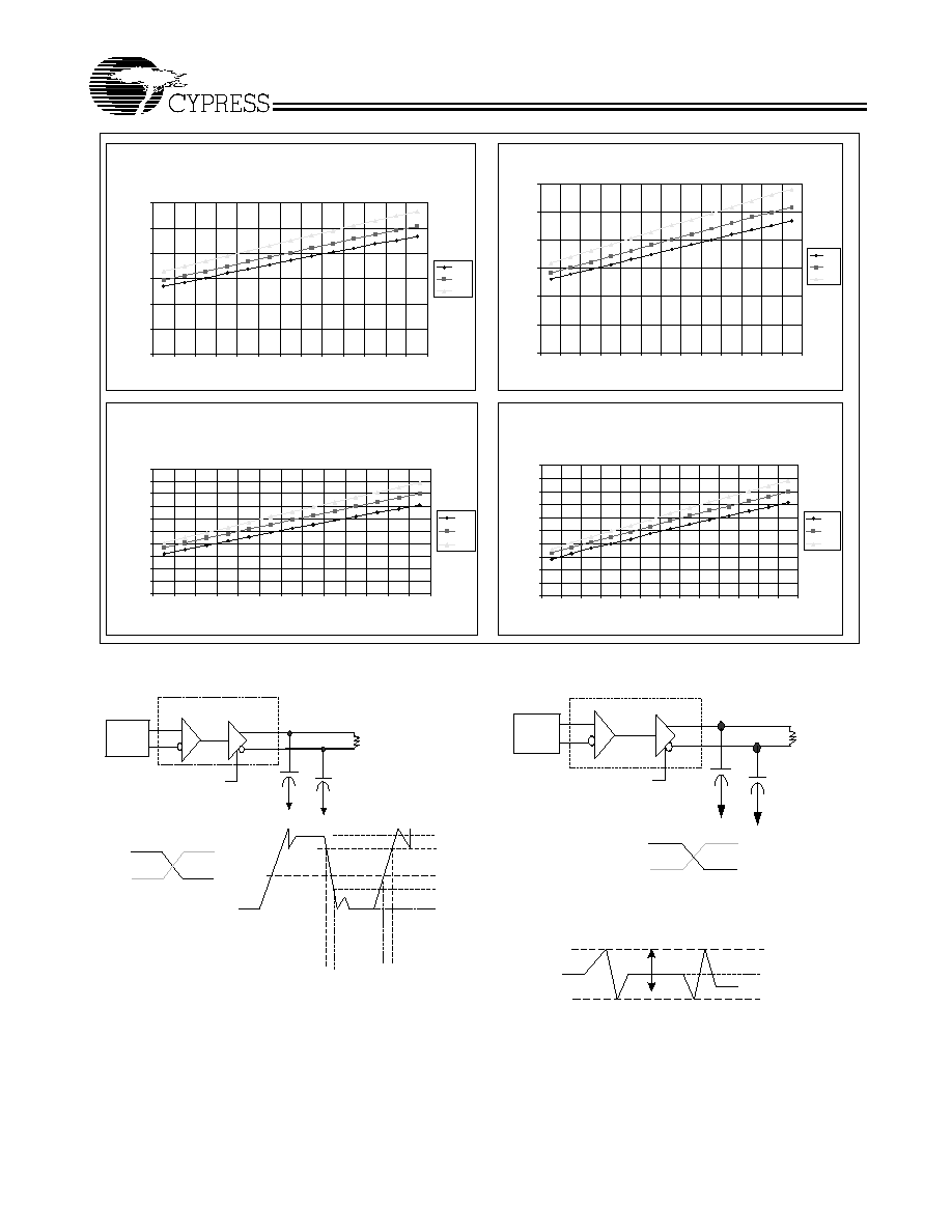
Dynamic Idd
VID=0.4V, VIC=1.2V, S0,S1=01;S2,S3=01
25∞C CY2LL8423
30.00
35.00
40.00
45.00
50.00
55.00
60.00
50
75
100
125
150
175
200
225
250
275
300
325
350
Fin (Mhz)
IDD (
m
A)
3.0V
3.3V
3.6V
Dynamic Idd
VID=0.4V, VIC=1.2V, S0,S1=00;S2,S3=00
25∞C CY2LL8423
40.00
45.00
50.00
55.00
60.00
65.00
70.00
75.00
80.00
85.00
90.00
50
75
100 125 150 175 200 225 250 275 300 325 350
Fin (Mhz)
I
DD (
m
A)
3.0V
3.3V
3.6V
Dynamic Idd
VID=0.4V, VIC=1.2V, S0,S1=01;S2,S3=01
25∞C CY2LL8423
40.00
45.00
50.00
55.00
60.00
65.00
70.00
75.00
80.00
85.00
90.00
50
75
100 125 150 175 200 225 250 275 300 325 350
Fin (Mhz)
i
dd (mA
)
3.0V
3.3V
3.6V
Dynamic Idd
VID=0.4V, VIC=1.2V, S0, S1=00;S2,S3=00
25∞C CY2LL8423
30.00
35.00
40.00
45.00
50.00
55.00
60.00
50
75
100
125
150
175
200
225
250
275
300
325
350
Fin (M hz)
I
DD (
m
A)
3.0V
3.3V
3.6V
Figure 2. Dynamic IDD Diagrams
A
B
R
Pulse
Generator
Y
Z
10 pF
DE
D
CL = 10pF
RL
0.0V
100%
80%
20%
0%
tR
tF
V
I(A)
V
I(B)
1.4V
1.0V
Figure 3. Test Circuit & Voltage Definitions for the
Differential Output Signal
[5,6,7]
Y
Z
10 pF
DE
D
CL = 10pF
RL
A
B
R
Pulse
Generator
Voc (ss)
V
DD
Voc (pp)
V
I(A)
V
I(B)
1.4V
1.0V
Figure 4. Test Circuit & Voltage Definitions for the Driver
Common-Mode Output Voltage
[5,6,7,8]