 | –≠–ª–µ–∫—Ç—Ä–æ–Ω–Ω—ã–π –∫–æ–º–ø–æ–Ω–µ–Ω—Ç: CY2PP3220 | –°–∫–∞—á–∞—Ç—å:  PDF PDF  ZIP ZIP |
PRELIMINARY
Dual 1:10 Differential Fanout Buffer
FastEdgeTM Series
CY2PP3220
Cypress Semiconductor Corporation
∑
3901 North First Street
∑
San Jose
,
CA 95134
∑
408-943-2600
Document #: 38-07513 Rev.*A
Revised April 15, 2003
Features
∑ Two sets of ten ECL/PECL differential outputs
∑ Two ECL-/PECL-differential inputs
∑ Hot-swappable/-insertable
∑ 50-ps output-to-output skew
∑ < 500-ps device-to-device skew
∑ Less than 10-ps intrinsic jitter
∑ 500-ps propagation delay (typical)
∑ Operation from DC to 1.5 GHz
∑ PECL supply range: V
CC
= 2.375V to 3.465V
with V
EE
= 0V
∑ ECL mode supply range: V
EE
= ≠2.375V to ≠3.465V
with V
CC
= 0V
∑ Industrial temperature range: ≠40
∞
C to 85
∞
C
∑ 52-pin 1.4-mm TQFP package
∑ Temperature compensation like 100K ECL
Description
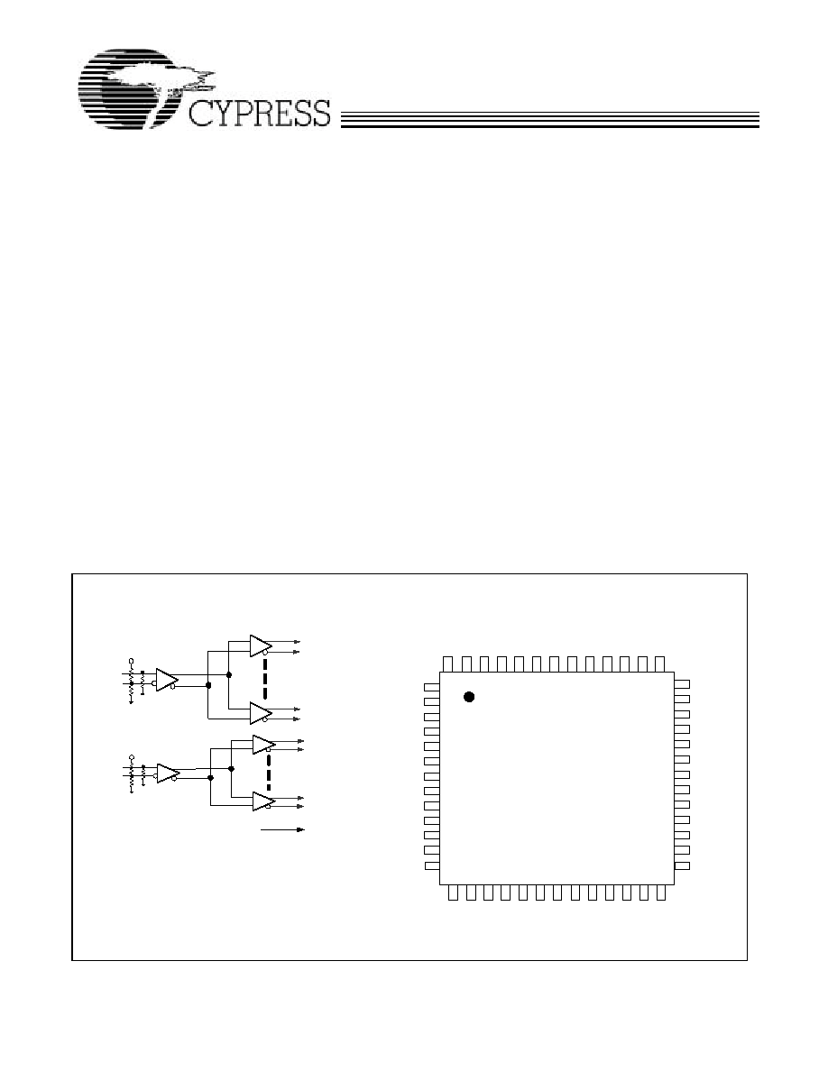
The CY2PP3220 is a low-skew, low propagation delay, dual
1-to-10 differential fanout buffer targeted to meet the require-
ments of high-performance clock and data distribution applica-
tions. The device is implemented on SiGe technology and has
a fully differential internal architecture that is optimized to
achieve low signal skews at operating frequencies of up to
1.5 GHz.
The device features two differential input paths which are
differential internally. The CY2PP3220 may function not only
as a differential clock buffer but also as a signal level translator
and fanout ECL/PECL single-ended or differential signals to
twenty ECL/PECL differential loads. An external bias pin, VBB,
is provided for distributing a single-ended signal. In such an
application, the VBB pin should be connected to either one of
the CLKA# or CLKB# inputs and bypassed to V
CC
via a
0.01-
µ
F capacitor. Traditionally, in ECL, it is used to provide
the reference level to a receiving single ended input that might
have a different self bias point.
Since the CY2PP3220 introduces negligible jitter to the timing
budget, it is the ideal choice for distributing high-frequency,
high-precision clocks across backplanes and boards in
communication systems. Furthermore, advanced circuit
design schemes, such as internal temperature compensation,
ensure that the CY2PP3220 delivers consistent, guaranteed
performance over differing platforms.
Block Diagram
Pin Configuration
CLKA
CLKA#
VCC
QA0
QA0#
QA9
QA9#
CLKB
CLKB#
VCC
QB0
QB0#
QB9
QB9#
VEE
VEE
VEE
VEE
VBB
CY2PP3220
40
41
42
43
44
45
46
47
48
49
50
51
52
QA0
QA1
QA0
#
QA1
#
QA2
QA2
#
QA3
QA3
#
QA4
QA4
#
QA5
QA5
#
VC
CO
39
38
37
36
35
34
33
32
31
30
29
28
27
QA6
QA7
QA6#
QA7#
QA8
QA8#
QA9
QA9#
QB0
QB0#
QB1
QB1#
VCCO
1
2
3
4
5
6
7
8
9
10
11
12
13
VCCO
VEE
VCC
CLKA
CLKA#
VBB
CLKB
CLKB#
VEE
QB9#
QB9
QB8#
QB8
26
25
24
23
22
21
20
19
18
17
16
15
14
V
CCO
QB
7
QB
7
#
QB
6
#
QB
6
QB
5
#
QB
5
QB
4
#
QB
4
QB
3
#
QB
3
QB
2
#
QB
2
PRELIMINARY
FastEdgeTM Series
CY2PP3220
Document #: 38-07513 Rev.*A
Page 2 of 11
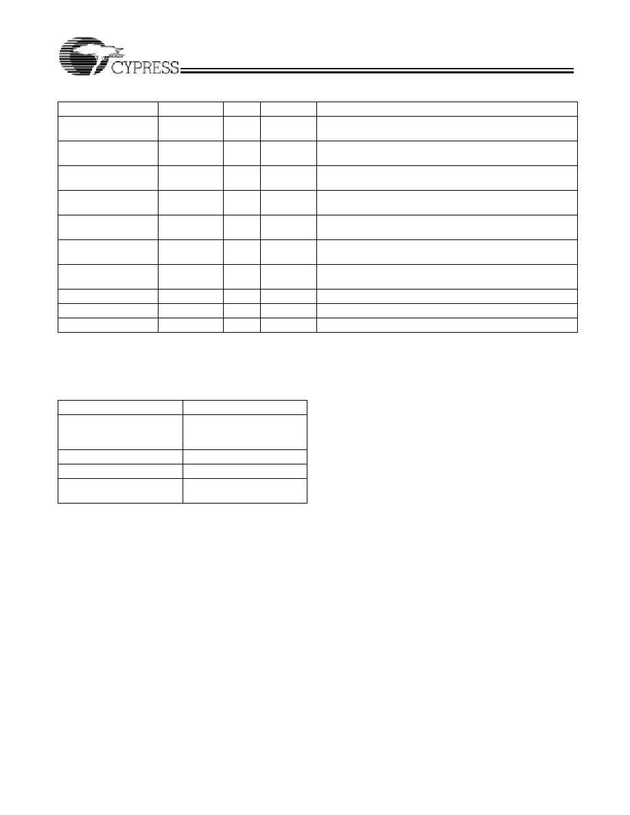
Governing Agencies
The following agencies provide specifications that apply to the
CY2PP3220. The agency name and relevant specification is
listed below.
Notes:
1.
In the I/O column, the following notation is used: I for Input, O for Output, PD for Pull-down, PU for Pull-up, PC for Pull Center, O for output, OS for open source
and PWR for Power.
2.
In ECL mode (negative power supply mode), V
EE
is either ≠3.3V or ≠2.5V and V
CC
is connected to GND (0V). In PECL mode (positive power supply mode),
V
EE
is connected to GND (0V) and V
CC
is either +3.3V or +2.5V. In both modes, the input and output levels are referenced to the most positive supply (V
CC
)
and are between VCC and VEE.
3.
V
BB
is available for use for single ended bias mode when V
CC
is +3.3V.
Pin Description
Pin
Name
I/O
Type
Description
4,5
CLKA, CLKA#
I,PD
[1]
I,PC
ECL/PECL Default Differential clock input pair
7,8
CLKB, CLKB#
I,PD
I,PC
ECL/PECL Alternate Differential clock input pair
52,50,48,46,44,42,39,3
7,35,33
QA(0:9)
O,OS
ECL/PECL True output
51,49,47,45,43,41,38,3
6,34,32
QA#(0:9)
O,OS
ECL/PECL Complement output
31,29,26,24,22,20,18,1
6,13,11
QB(0:9)
O,OS
ECL/PECL True output
30,28,25,23,21,19,17,1
5,12,10
QB#(0:9)
O,OS
ECL/PECL Complement output
6
VBB
[3]
O
Bias
Reference voltage output for single ended ECL or PECL
operation
3,9
VEE
[2]
≠PWR
Power
Power supply, negative connection
2
VCC
+PWR
Power
Power supply, positive connection
1,14,27,40
VCCO
+PWR
Power
Power supply, positive connection
Agency Name
Specification
JEDEC
JESD 51 (Theta JA)
JESD 8≠2 (ECL)
JESD 65≠A (skew,jitter)
IEEE
1596.3 (Jitter specs)
UL
94 (Flammability)
Mil≠Spec
883E Method 1012.1
(Thermal Theta JC)
PRELIMINARY
FastEdgeTM Series
CY2PP3220
Document #: 38-07513 Rev.*A
Page 3 of 11
Absolute Maximum Conditions
Parameter
Description
Condition
Min.
Max.
Unit
V
CC
Supply Voltage
Non-functional
≠0.3
4.6
VDC
V
CC
Operating Voltage
Functional
2.5 ≠ 5%
3.3 + 5%
VDC
V
BB
Output Reference Voltage
Relative to V
CC
V
CC
≠1.525
V
CC
≠1.325
VDC
I
BB
Output Reference Current
Relative to V
BB
200
uA
VTT
Output Termination Voltage
VTT = 0V for V
CC
= 2.5V
V
CC
≠2
VDC
V
IN
Input Voltage
Relative to V
CC
≠0.3
V
CC
+0.3
VDC
V
OUT
Output Voltage
Relative to V
CC
≠0.3
V
CC
+0.3
VDC
LU
I
Latch Up Immunity
Functional
300
mA
T
S
Temperature, Storage
Non-Functional
≠65
150
∞C
T
A
Temperature, Operating Ambient
Functional
≠40
85
∞C
ÿ
Jc
Dissipation, Junction to Case
Functional
TBD
TBD
∞C/W
ÿ
Ja
Dissipation, Junction to Ambient
Functional
40
60
∞C/W
ESD
h
ESD Protection (Human Body Model)
2000
V
M
SL
Moisture Sensitivity Level
TBD
N.A.
G
ATES
Total Functional Gate Count
Assembled Die
50
Ea.
UL≠94
Flammability Rating
At 1/8 in.
V≠0
N.A.
FIT
Failure in Time
Manufacturing test
1
ppm
PECL DC Electrical Specifications
Parameter
Description
Condition
Min.
Max.
Unit
V
CC2.5V
2.5 Operating Voltage
2.5V ± 5%, V
EE
= 0.0V
2.375
2.625
V
V
CC3.3V
3.3 Operating Voltage
3.3V ± 5%, V
EE
= 0.0V
3.135
3.465
V
V
IL
Input Voltage, Low
V
CC
≠1.945
V
CC
≠1.625
V
V
IH
Input Voltage, High
Define V
CC
and load current
V
CC
≠1.165
V
CC
≠0.880
V
I
IN
Input Current
[4]
V
IN
= [VILmin=2.406V or
V
IH
≠ax=1.655V] at VCC=3.6V
200
uA
Clock Input Pair CLKA, CLKA#, CLKB1, CLKB1#(PECL Differential Signals)
V
PP
Differential input voltage
[5]
Differential operation
0.1
1.3
V
V
CMR
Differential cross point voltage
[6]
Differential operation
1.2
V
CC
V
I
IN
Input Current
[4]
V
IN
= V
IL
or V
IN
= V
IH
200
uA
PECL Outputs QA((0:9),#),QB((0:9),#)(PECL Differential Signals)
V
OH
Output High Voltage
I
OH
= ≠30 mA
[7]
(50
Load)
V
CC
≠1.145
V
CC
≠0.895
V
V
OL
Output Low Voltage
V
CC
= 3.3V ± 5%
V
CC
= 2.5V ± 5%
I
OL
= ≠5 ma
[7]
(50
Load)
V
CC
≠1.945
V
CC
≠1.945
V
CC
≠1.695
V
CC
≠1.695
V
Supply Current and VBB
I
EE
Maximum Quiescent Supply Current
without output termination current
[7]
VEE pin
≠
260
mA
V
BB
Output reference voltage
IBB = 200 uA
V
CC
≠1.525
V
CC
≠1.325
V
I
PUP
Internal Pull-up Current
TBD
TBD
mA
I
PDWN
Internal Pull-down Current
TBD
TBD
mA.
Notes:
4.
Input have internal pullup / pulldown or biasing resistors which affect the input current.
5.
VPP (DC) is the minimum differential input voltage swing required to maintain device functionality.
6.
VCMR (DC) is the crosspoint of the differential input signal. Functional operation is obtained when the crosspoint is within the VCMR (DC) range and the input
swing lies within the VPP (DC) specification.
7.
Equivalent to a termination of 50
to VTT.
PRELIMINARY
FastEdgeTM Series
CY2PP3220
Document #: 38-07513 Rev.*A
Page 4 of 11
C
IN
Input pin capacitance
TBD
TBD
pF
C
OUT
Output pin capacitance
TBD
TBD
pF
L
IN
Pin Inductance
TBD
TBD
nH
Z
OUT
Output impedance
TBD
TBD
ECL DC Electrical Specifications
Parameter
Description
Condition
Min.
Max.
Unit
V
EE
≠2.5 Negative Power Supply
≠2.5V ± 5%, V
EE
= 0.0V
≠2.375
≠2.625
V
V
EE
≠3.3 Negative Power Supply
≠3.3V ± 5%, V
EE
= 0.0V
≠3.135
≠3.465
V
V
IL
Input Voltage, Low
≠1.945
≠1.625
V
V
IH
Input Voltage, High
Define V
CC
and load current
≠1.165
≠0.880
V
I
IN
Input Current
[4]
V
IN
= V
IL
or Vin = V
IH
200
uA
Clock Input Pair CLKA,CLKA#,CLKB,CLKB# (ECL Differential Signals)
V
PP
Differential input voltage
[5]
Differential operation
0.1
1.3
V
V
CMR
Differential cross point voltage
[6]
Differential operation
V
EE
+1.2
0
V
I
IN
Input Current
[4]
V
IN
= V
IL
or V
IN
= V
IH
200
uA
ECL Outputs QA((0:9),#),QB((0:9),#) (ECL Differential Signals)
V
OH
Output High Voltage
I
OH
= ≠30 mA
[7]
≠1.145
≠0.895
V
V
OL
Output Low Voltage
V
EE
= ≠3.3V ± 5%
V
EE
= ≠2.5V ± 5%
I
OL
= ≠5 ma
[7]
≠1.945
≠1.945
≠1.695
≠1.3
V
Supply Current and VBB
I
EE
Maximum Quiescent Supply Current
without output termination current
[8]
V
EE
pin
130
mA
V
BB
Output reference voltage
I
BB
=200 uA
≠1.525
≠1.325
V
AC Electrical Specifications
Parameter
Description
Condition
Min.
Max.
Unit
Clock input pair CLKA, CLKA#, CLKB,CLKB# (PECL or ECL differential signals)
V
PP
Differential input voltage
[10]
Differential Operation
0.1
1.3
V
V
CMR
Differential cross point voltage
[11]
Differential Operation
V
EE
+1.2
0
V
F
IN
Input Frequency
[12]
50% Duty Cycle Standard load
1500
MHz
T
PD
Propagation Delay CLKA or CLKB to
QA((0:4),#),QB((0:4),#) pairs
660-MHz 50% Duty Cycle Standard Load
Differential Operation
400
750
ps
Clock Outputs QA((0:9),#),QB((0:9),#)
Vo
(P-P)
Differential output voltage
(peak-to-peak)
Differential PRBS
fo < 50 MHz
fo < 0.8 GHz
fo < 1.0 GHz
0.45
0.4
0.375
≠
V
V
CMR
Common Voltage Range
V
CC
≠1.425
V
Notes:
8.
I
CC
Calculation: ICC = (number of differential output pairs used) x (I
OH
+ I
OL
) + IEE or I
CC
= (number of differential output pairs used) x (V
OH
≠VTT)/Rload +
(V
OL
≠VTT)/Rload +I
EE
.
9.
AC characteristics apply for parallel output termination of 50
to VTT.
10. VPP (AC) is the minimum differential ECL/PECL input swing required to maintain AC characteristics including tpd and device-to-device skew.
11.
VCMR (AC) is the crosspoint of the differential ECL/PECL input signal. Normal AC operation is obtained when the crosspoint is within the VCMR(AC) range
and the input swing lies within the VPP(AC) specification. Violation of VCMR(AC) or VPP(AC) impacts the device propagation delay, device and part-to-part
skew.
12. The CY2PP3220 is fully operation up to 1.5 GHz.
PECL DC Electrical Specifications
(continued)
Parameter
Description
Condition
Min.
Max.
Unit
PRELIMINARY
FastEdgeTM Series
CY2PP3220
Document #: 38-07513 Rev.*A
Page 5 of 11
Timing Definitions
Note:
13. Output pulse skew is the absolute difference of the propagation delay times: | tPLH ≠ tPHL |.
tsk
(O)
Output-to-output skew
660-MHz 50% duty cycle Standard load
Differential Operation
≠
50
ps
tsk
(PP)
Output-to-output skew (part-to-part)
660-MHz 50% duty cycle Standard load
Differential Operation
≠
500
ps
t
CCJ
Output cycle-to-cycle jitter (Intrinsic)
660-MHz 50% duty cycle Standard load
Differential Operation
TBD
TBD
ps
tsk
(P)
Output pulse skew
[13]
660-MHz 50% duty cycle Standard load
Differential Operation
TBD
TBD
ps
T
R
,T
F
Output Rise/Fall time
660-MHz 50% duty cycle Differential 20% to
80%
≠
0.3
ns
TTB
Total Timing Budget
660-MHz 50% duty cycle Standard load
TBD
TBD
ps
D
J
Deterministic/Intrinsic Jitter
660-MHz 50% duty cycle Standard load
≠
10
ps
r.m.s.
AC Electrical Specifications
(continued)
Parameter
Description
Condition
Min.
Max.
Unit
V IH
V IL
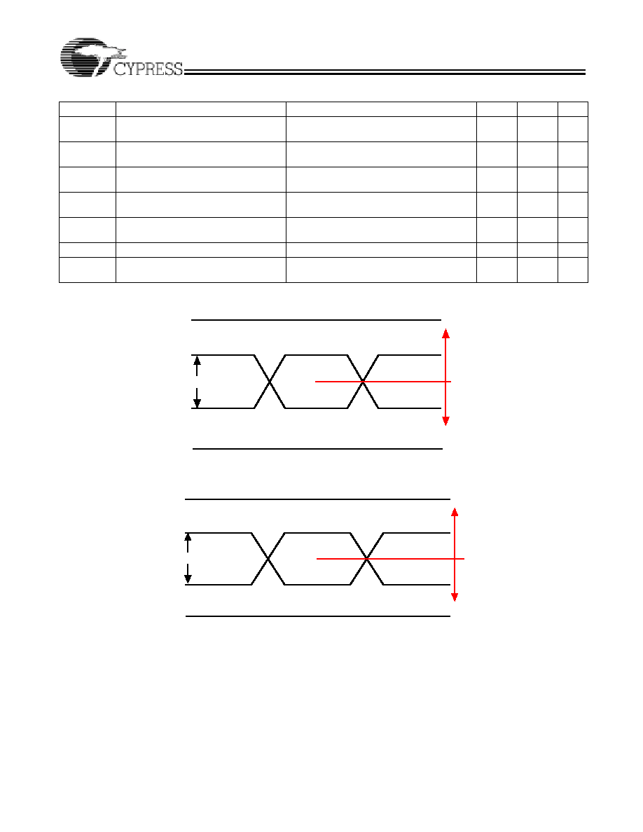
V C M R
V P P
V C M R M in = 1 .2 V
V P P ra n g e
0 .1 V - 1 .3 V
V C M R M a x = V C C
V C C = 2 .5 V or 3 .3 V
VC C
G N D
G N D = 0 .0 V
Figure 1. PECL Waveform Definitions
V
IH
V
IL
V
C M R
V P P
V C C
V E E
V C C = 0 .0 V
V C M R m a x = 0
V C M R m in = V E E -1 .2 V
V E E = -2 .5 V o r - 3 .3 V
V P P r a n g e = 0 .1
to 1 .3 V
Figure 2. ECL Differential Waveform Definitions