Äîêóìåíòàöèÿ è îïèñàíèÿ www.docs.chipfind.ru
13-Bit to 26-Bit Registered Buffer
PC2700-/PC3200-Compliant
CY2SSTV16859
Cypress Semiconductor Corporation
·
3901 North First Street
·
San Jose
,
CA 95134
·
408-943-2600
Document #: 38-07463 Rev. *B
Revised July 29, 2003
Features
· Differential clock inputs up to 280 MHz
· Supports LVTTL switching levels on the RESET# pin
· Output drivers have controlled edge rates, so no
external resistors are required.
· Two KV ESD protection
· Latch-up performance exceeds 100 mA per JESD78,
Class II
· 64-pin TSSOP/JEDEC and 56-pin QFN package avail-
ability
· JEDEC specification supported
Description
This 13-bit to 26-bit registered buffer is designed for 2.3V to
2.7 VDD operations.
All inputs are compatible with the JEDEC Standard for SSTL-2,
except the LVCMOS reset (RESET#) input. All outputs are
SSTL_2, Class II compatible.
The CY2SSTV16859 operates from a differential clock (CLK
and CLK#) of frequency up to 280 MHz. Data are registered at
crossing of CLK going high and CLK# going low.
When RESET# is low, the differential input receivers are
disabled, and undriven (floating) data and clock inputs are
allowed. The LVCMOS RESET# input must always be held at
a valid logic high or low level.
To ensure defined outputs from the register before a stable
clock has been supplied, RESET# must be held in the low
state during power up.
In the DDR DIMM application, RESET# is completely
asynchronous with respect to CLK# and CLK. Therefore, no
timing relationship can be guaranteed between the two. When
entering reset, the register is cleared and the outputs are
driven low quickly, relative to the time to disable the differential
input receivers, thus ensuring no glitches on the output.
However, when coming out of reset, the register becomes
active quickly, relative to the time to enable the differential
input receivers.
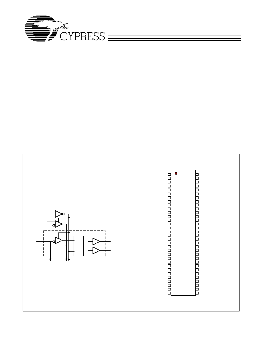
Block Diagram
Pin Configuration
D1
VREF
CLK #
Q1A
Q1B
To 12 Other Channels
CLK
RESET #
D
C
R
1
2
3
4
5
6
7
8
9
10
11
12
13
14
15
16
17
18
19
20
21
22
23
24
25
26
27
28
29
30
31
32
Q13A
Q12A
Q11A
Q10A
Q9A
VDDQ
GND
Q8A
Q7A
Q6A
Q5A
Q4A
Q3A
Q2A
GND
Q1A
Q13B
VDDQ
Q12B
Q11B
Q10B
Q9B
Q8B
Q7B
Q6B
GND
VDDQ
Q5B
Q4B
Q3B
Q2B
Q1B
64
63
62
61
60
59
58
57
56
55
54
53
52
51
50
49
48
47
46
45
44
43
42
41
40
39
38
37
36
35
34
33
C
Y
2
SST
V1
6859
VDDQ
GND
D13
D12
VDD
VDDQ
GND
D11
D10
D9
GND
D8
D7
RESET #
GND
CLK #
CLK
VDDQ
VDD
VREF
D6
GND
D5
D4
D3
GND
VDDQ
VDD
D2
D1
GND
VDDQ
64 TSSOP Package
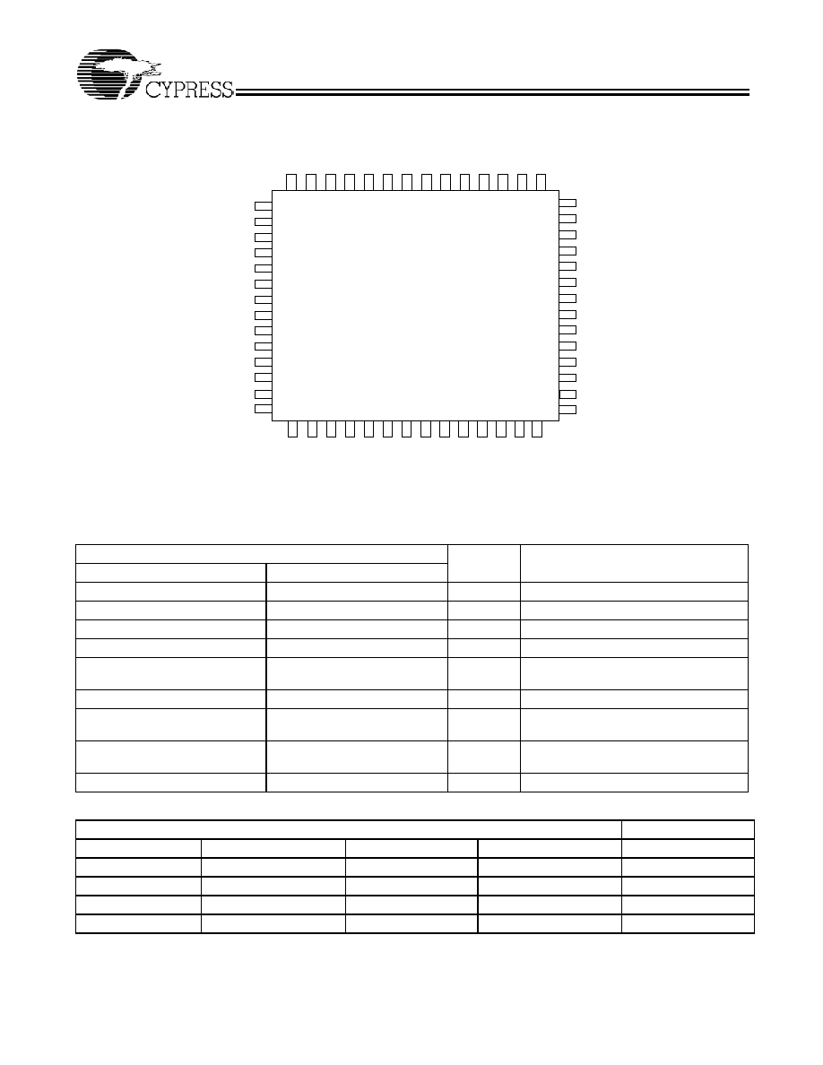
CY2SSTV16859
Document #: 38-07463 Rev. *B
Page 2 of 8
Pin Configuration
(continued)
56 QFN Package
1
2
3
4
5
6
7
8
9
10
11
12
13
Q7A
Q5A
Q6A
Q4A
Q3A
Q2A
Q1A
Q13B
VDDQ
Q12B
Q11B
Q10B
Q9B
14
Q8B
27
26
25
24
23
22
21
20
19
18
17
16
15
Q7B
VDDQ
Q6B
Q5B
Q4B
Q3B
Q2B
Q1B
VDDQ
D1
D2
VD
D
VDDQ
28
D3
42
41
40
39
38
37
36
35
34
33
32
31
30
D10
D8
D9
D7
RESET#
GND
CLK#
CLK
VDDQ
VDD
VREF
D6
D5
29
D4
44
45
46
47
48
49
50
51
52
53
54
55
56
Q8A
Q9A
VDD
Q
Q10A
Q11A
Q12A
Q13A
VDD
Q
GN
D
D13
D12
VDD
VDD
Q
43
D11
Pin Description
Pin Name
Description
TSSOP
QFN
51
38
RESET#
Disable Clocking and Reset Latch
7,15,34,39,43,50,54,58,63
37,48
GND
Ground
37,46,60
26,33,45
VDD
Supply Voltage
6,18,27,33,38,47,59,64
9,17,23,27,34,44,49,55
VDDQ
Supply Voltage, Quiet
45
32
VREF
Reference Voltage for Data Inputs
D(1:13)
16,14,13,12,11,10,9,8,5,4,3,2,1
7,6,5,4,3,2,1,56,54,53,52,51,50
QA(1:13)
Data Outputs
32,31,30,29,28,25,24,23,22,21,20,
19,17
22,21,20,19,18,16,15,14,13,12
11,10,8
QB(1:13)
Data Outputs
35,36,40,41,42,44,52,53,55,56,57,
61,62
24,25,28,29,30,31,39,40,41,42
43,46,47
D(1:13)
Data Inputs
48,49
35,36
CLK, CLK# Differential Clock Signals
Table 1. Function Table
[1,2,3]
INPUTS
OUTPUT
RESET#
CLK
CLK#
D
Q
H
L
L
H
H
H
H
L or H
L or H
X
Q
0
L
X or floating
X or floating
X or floating
L
Notes:
1.
H = High voltage level.
2.
L = Low voltage level.
3.
X = Don't care.
CY2SSTV16859
Document #: 38-07463 Rev. *B
Page 3 of 8
Absolute Maximum Conditions
[4,5]
Parameter
Description
Condition
Min.
Max.
Unit
V
TERM
[6]
Terminal Voltage with respect to V
SS
0.5
3.6
V
V
TERM
[7]
Terminal Voltage with respect to V
SS
0.5
V
DD
+ 0.5
V
T
STG
Storage Temperature
65°
150°C
°C
I
OUT
DC Output Current
50
50
mA
I
IK
Continuous Clamp Current
V
I
<0 or V
I
>V
SS
50
50
mA
I
OK
Continuous Clamp Current
V
O
<0 or V
O
>V
DD
50
50
mA
I
dd
I
SS
Continuous Current through each V
DD,
V
DDQ
or V
SS
100
100
mA
Recommended Operating Conditions
[8]
Parameter
Description
Min.
Typ.
Max.
Unit
V
DD
Supply voltage
2.3
2.5
2.7
V
V
DDQ
Output supply voltage PC1600,PC2100,PC2700
2.3
2.5
2.7
V
PC3200
2.5
2.6
2.7
V
V
REF
Reference voltage
(V
REF
= V
DDQ
/2)
PC1600,PC2100,PC2700
1.15
1.25 1.35
V
PC3200
1.25
1.3
1.35
V
V
TT
Termination voltage
V
REF
40 mV
V
REF
V
REF
+ 40 mV
V
V
I
Input voltage
0
V
DD
V
V
IH
AC Data Input high-level voltage
V
REF
+ 310 mV
V
V
IL
AC Data Input low-level voltage
V
REF
310 mV
V
V
IH
DC Data Input high-level voltage
V
REF
+ 150 mV
V
V
IL
DC Data Input low-level voltage
V
REF
150 mV
V
V
IH
RESET# Input high-level voltage
1.7
V
V
IL
RESET# Input low-level voltage
0.7
V
V
ICR
CLK, CLK# Common-mode input voltage range
0.97
1.53
V
V
I(PP)
CLK, CLK# Peak-to-peak input voltage
360
mV
I
OH
High-level output current
20
mA
I
OL
Low-level output current
20
mA
T
A
Operating free-air temperature
0
85
°C
DC Electrical Specifications
Parameter
Description
Condition
VDD
Min.
Typ.
[9]
Max. Unit
V
IK
Clamp Voltage
I
I
= 18 mA
2.3V
1.2
V
V
OH
High level output
voltage
I
OH
= 100 µA
2.3 to 2.7V
V
DD
0.2
V
I
OH
= 16 mA
2.3V
1.95
V
V
OL
Low level output
voltage
I
OL
= 100 µA
2.3 to 2.7V
0.2
V
I
OL
= 16 mA
2.3
0.35
V
I
I
All Inputs
V
I
= V
DD
or V
SS
2.7V
± 5
µA
I
DD
Static Standby
RESET# = V
SS
I
O
= 0
2.7V
10
µA
Static Operating RESET# = V
DD
, V
I
= V
IH(AC)
or V
IL(AC)
2.7
40.0
mA
Notes:
4.
The voltage on any input or I/O pin cannot exceed the power pin during power-up. Power supply sequencing is NOT required.
5.
Stresses greater than those listed under Absolute Maximum Conditions may cause permanent damage to the device. This is a stress rating only and functional
operation of the device at these or any other conditions above those indicated in the operational sections of this specification is not implied. Exposure to absolute
maximum rating conditions for extended period may affect reliability.
6.
V
DD
/V
DDQ
terminals.
7.
All terminals except V
DD
.
8.
The RESET# input of the device must be held at V
DD
or V
SS
to ensure proper device operation.
9.
All typical values are measured at T
AMB
= 25°C
CY2SSTV16859
Document #: 38-07463 Rev. *B
Page 4 of 8
I
DDD
Dynamic
operating clock
only
RESET# = V
DD
, V
I
= V
IH(AC)
or V
IL(AC),
CLK and CLK# switching 50% duty
cycle
I
O
= 0
2.7V
30.0
µA/
clock
MHz
Dynamic
operating per
each data input
RESET# = V
DD
, V
I
= V
IH(AC)
or V
IL(AC),
CLK and CLK# switching 50% duty
cycle. One data input switching at half
clock frequency, 50% duty cycles.
2.7
15.0
µA/
clock
MHz
/data
input
r
OH
Output high
I
OH
= 20 mA
2.3 to 2.7V
7
20
r
OL
Output low
I
OL
= 20 mA
2.3 to 2.7V
7
20
r
O(
)
|r
OH
r
OL
| each
separate bit
I
O
= 20 mA, T
A
= 25°C
2.5V
4
C
i
Data Inputs
V
I
= V
REF
+ 310 mV
2.5
2.5
3.5
pF
CLK and CLK#
V
ICR
= 1.25V, V
I(PP)
= 360 mV
2.5
2.5
3.5
pF
RESET#
V
I
= V
DD
or V
SS
2.5
2.5
3.5
pF
AC Electrical Specifications
Parameter
Description
V
DD
= 2.5V± 0.2V
Unit
Min.
Max.
f
clock
Clock Frequency
280
MHz
t
w
Pulse duration, CLK, CLK# high or low
2.0
ns
t
act
Differential inputs active time (data inputs must be held low after RESET# is taken high).
22
ns
t
inact
Differential inputs inactive time (data and clock inputs must be held at valid levels
(not floating) after RESET# is taken low).
22
ns
t
su
Set-up time, fast slew rate
[10, 12]
Data before CLK
, CLK#
0.75
ns
Set-up time, slow slew rate
[11, 12]
0.9
ns
t
h
Hold time, fast slew rate
[10, 12]
Data after CLK
, CLK#
0.75
ns
Hold time, slow slew rate
[11, 12]
0.9
ns
Table 2. Switching Characteristics Over Recommended Operating Conditions
[13]
Parameter
From (Input)
To (Output)
V
DD
= 2.5V ± 0.2V
Unit
Min.
Max.
f
max
280
MHz
t
PHL
RESET#
Q
5
ns
t
PD
CLK and CLK#
Q
1.1
2.8
ns
Notes:
10. For data signal input slew rate
1 V/ns.
11. For data signal input slew rate
V/ns and < 1V/ns.
12. CLK and CLK# signals input slew rates are
1 V/ns.
13. See test circuits and waveforms. TA = 0°C to +85°C.
DC Electrical Specifications
(continued)
Parameter
Description
Condition
VDD
Min.
Typ.
[9]
Max. Unit
CY2SSTV16859
Document #: 38-07463 Rev. *B
Page 5 of 8
Output Buffer Characteristics
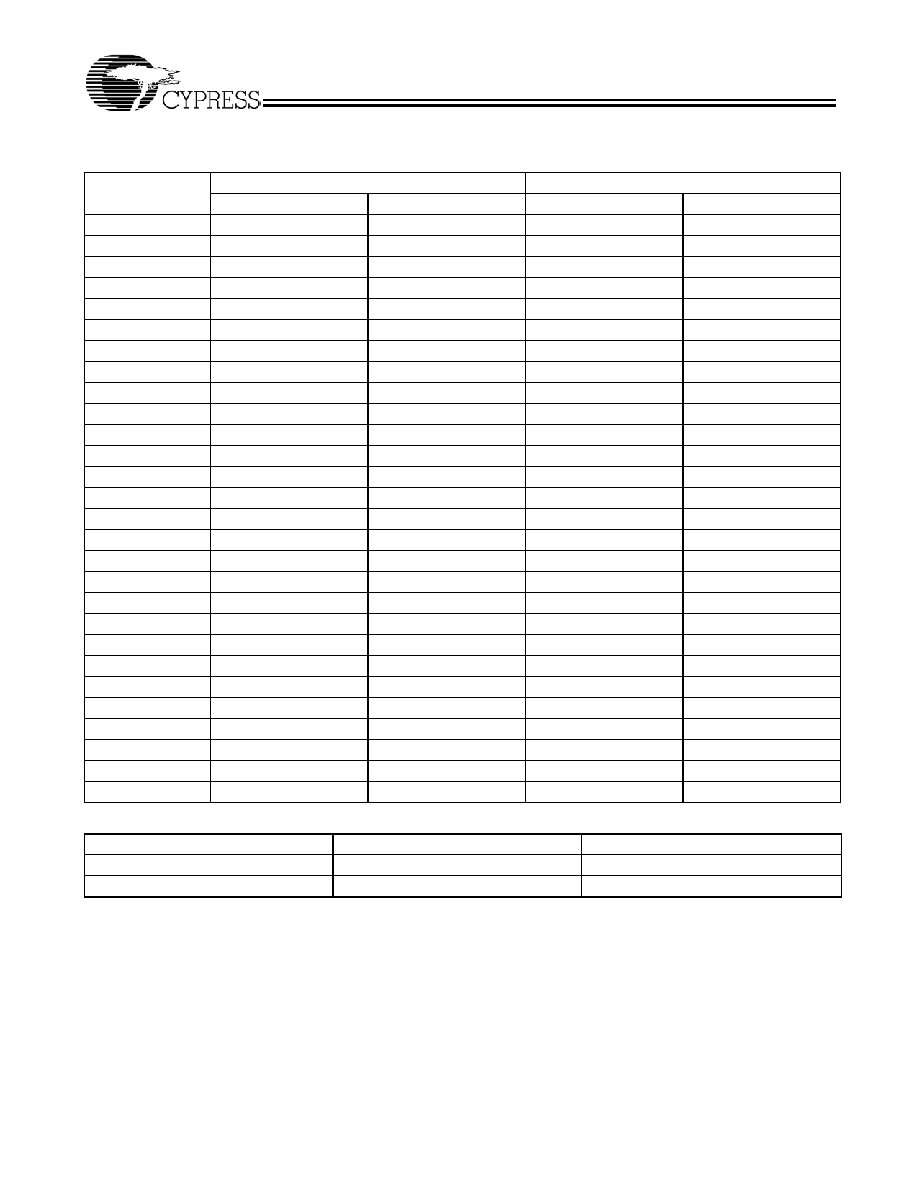
Table 3. Output Buffer Voltage vs. Current (V/I) Characteristics
Voltage (V)
Pull-Down
Pull-Up
Min. I(mA)
Max. I(mA)
Min. I(mA)
Max. I(mA)
0
0
0
55
162
0.1
6
13
55
161
0.2
10
25
54
160
0.3
15
38
54
159
0.4
19
49
54
157
0.5
23
60
54
156
0.6
27
71
53
154
0.7
30
81
53
152
0.8
34
91
53
149
0.9
36
100
52
146
1.0
38
108
52
143
1.1
40
115
52
140
1.2
42
123
51
137
1.3
43
130
50
134
1.4
44
137
48
130
1.5
44
144
46
125
1.6
45
150
44
120
1.7
45
158
40
112
1.8
45
165
38
104
1.9
45
172
35
96
2.0
45
179
31
83
2.1
46
185
28
72
2.2
46
191
23
60
2.3
46
196
19
49
2.4
46
201
15
38
2.5
46
206
10
27
2.6
46
211
5
15
2.7
46
216
0
0
Table 4. Output Buffer Slew-Rate Characteristics
dV/dt
Min.
Max.
Rise
0.85 V/ns
15.9 V/ns
Fall
1.00 V/ns
18.9 V/ns