
Differential Clock Buffer/Driver
CY2SSTV8575
Cypress Semiconductor Corporation
∑
3901 North First Street
∑
San Jose
∑
CA 95134
∑
408-943-2600
Document #: 38-07458 Rev. **
Revised October 30, 2002
TV8575
Features
∑ Operating frequency: 60 MHz to 170 MHz
∑ Supports 266-MHz DDR SDRAM
∑ 5 differential outputs from 1 differential input
∑ Spread Spectrum compatible
∑ Low jitter (cycle-to-cycle): < 75
∑ Very low skew: < 100 ps
∑ Power Management Control input
∑ High-impedance outputs when input clock < 20 MHz
∑ 2.5V operation
∑ 32-pin TQFP JEDEC MS-026 C
Description
The CY2SSTV8575 is a high-performance, low-skew, low jitter
zero-delay buffer designed to distribute differential clocks in
high-speed applications. The CY2SSTV8575 generates five
differential pair clock outputs from one differential pair clock
input. In addition, the CY2SSTV8575 features differential
feedback clock outputs and inputs. This allows the
CY2SSTV8575 to be used as a zero-delay buffer.
When used as a zero-delay buffer in nested clock trees, the
CY2SSTV8575 locks onto the input reference and translates
with near zero delay to low-skew outputs.
Block Diagram
Pin Configuration
16
2
1
12
11
15
27
28
30
31
18
19
Test and
Powerdown
Logic
PLL
5
6
21
22
FBI
N
FBIN
#
CLK
CLK#
AVDD
23
8
OE
Y0
Y0#
Y1
Y1#
Y2
Y2#
Y3
Y3#
Y4
Y4#
FBOUT
FBOUT#
TQFP-32
JEDEC MS-026 C
Y2#
Y2
VSS
VDDQ
Y1
Y1#
VSS
AVSS
Y0#
Y0
V
DDQ
CK
CK
#
AV
D
D
V
DDQ
V
DDQ
VDDQ
VSS
Y4#
Y4
Y3#
Y3
VDDQ
VSS
VSS
OE
FB
IN
VD
D
Q
FB
O
U
T#
VSS
FB
I
N
#
FB
O
U
T
CY2SSTV8575
1
2
3
4
5
6
7
8
9 10 11
12 13 14 15 1
6
24 23 22 21 20 19 18 17
32 31
30
29
28 27
26
25

CY2SSTV8575
Document #: 38-07458 Rev. **
Page 2 of 8
Pin Description
Pin
Name
I/O
Type
Description
5,6
CLK, CLK#
I
LV Differential Input
Differential Clock Input
21
FBIN#
I
Differential Input
Feedback Clock Input. Connect to FBOUT# for accessing the
PLL.
22
FBIN
I
Feedback Clock Input. Connect to FBOUT for accessing the
PLL.
2,12,15,27,30
Y(0:4)
O
Differential Outputs
Clock + Outputs
1,11,16,28,31
Y(0:4)#
O
Clock ≠ Outputs
18
FBOUT
O
Differential Outputs
Feedback Clock Output. Connect to FBIN for normal
operation. A bypass delay capacitor at this output will control
Input Reference/Output Clocks phase relationships.
19
FBOUT#
O
Feedback Clock Output. Connect to FBIN# for normal
operation. A bypass delay capacitor at this output will control
Input Reference/Output Clocks phase relationships.
23
OE
I
Output Enable Input. When OE is set HIGH, all Q and Q#
outputs are enabled and switch at the same frequency as CLK.
When set LOW, all Q and Q# outputs are disabled (Hi-Z) and
the PLL is powered down.
3,4,7,13,20,26,
29
VDDQ
2.5V Nominal
2.5V Power Supply for Output Clock Buffers
8
AVDD
2.5V Nominal
2.5V Power Supply for PLL. When AVDD is at GND, PLL is
bypassed and CLK is buffered directly to the device outputs.
During disable (OE = 0), the PLL is powered down.
10,14,17,24,25,
32
VSS
0.0V Ground
Common Ground
9
AVSS
0.0V Analog Ground
Analog Ground
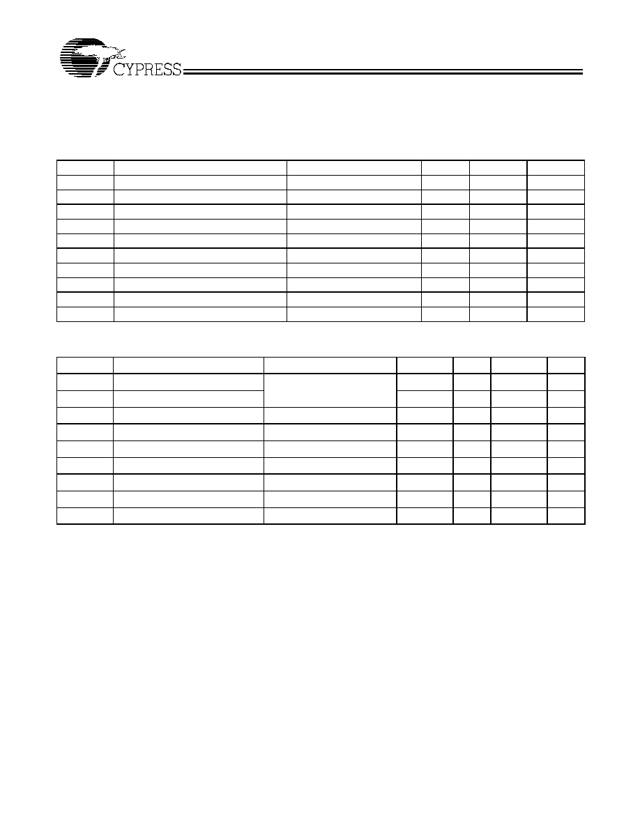
Table 1. Function Table
INPUTS
OUTPUTS
PLL
AVDD
OE
CLK
CLK#
Y
Y#
FBOUT
FBOUT#
GND
H
L
H
L
H
L
H
BYPASSED/OFF
GND
H
H
L
H
L
H
L
BYPASSED/OFF
X
L
L
H
Z
Z
Z
Z
Off
X
L
H
L
Z
Z
Z
Z
OFF
2.5V
H
L
H
L
H
L
H
On
2.5V
H
H
L
H
L
H
L
On
2.5V
H
< 20 MHz
< 20 MHz
Hi-Z
Hi-Z
Hi-Z
HI-Z
Off

CY2SSTV8575
Document #: 38-07458 Rev. **
Page 3 of 8
Power Management Functions
Output enable/disable control of the CY2SSTV8575 allows the
user to implement power management schemes into the de-
sign. Outputs are three-stated/disabled when OE is asserted
low, see Table 1. The enabling and disabling of outputs is done
in such a manner to eliminate the possibility of the partial "runt"
clocks.
Zero Delay Buffer
When used as a zero delay buffer the CY2SSTV8575 will likely
be in a nested clock tree application. For these applications
the CY2SSTV8575 offers a differential clock input pair as a
PLL reference. The CY2SSTV8575 can lock onto the refer-
ence and translate with near zero delay to low-skew outputs.
For normal operation, the external feedback input, FBIN, is
connected to the feedback output, FBOUT. By connecting the
feedback output to the feedback input the propagation delay
through the device is eliminated. The PLL works to align the
output edge with tine input reference edge thus producing a
near zero delay. The reference frequency affects the static
phase offset of the PLL and thus the relative delay between
the inputs and outputs.
When AVDD is strapped LOW, the PLL is turned off and by-
passed for test purposes.
Figure 1. Clock Structure 1
[1]
Note:
1.
Output load capacitance for 2 DDR-SDRAM loads: 5 pF <
CL <
8 pF.
PLL
FBIN
FBIN#
120 Ohm
120 Ohm
CLK
CLK#
DDR -
SDRAM
120 Ohm
VTR
VCP
0.3"
= 2.5"
= 0.6" (Split to Terminator)
DDR _SDRAM
represents a capacitive
load
DDR -
SDRAM
FBOUT#
FBOUT
Yx
Yx#

CY2SSTV8575
Document #: 38-07458 Rev. **
Page 4 of 8
Figure 2. Clock Structure 2
[2]
Figure 3. Differential Signal Using Direct Termination Resistor
Governing Agencies
The following agencies provide specifications that apply to the CY2SSTV8575. The agency name and relevant specification is
listed below;
Agency Name
Specification
JEDEC
MS - 026-C
Note:
2.
Output load capacitance for 4 DDR-SDRAM loads: 10 pF <
CL <
16 pF.
DDR-SDRAM
PLL
FBIN
FBIN#
120 Ohm
120 Ohm
CLK
CLK#
DDR-SDRAM
Stack
DDR-SDRAM
Stack
120 Ohm
VTR
VCP
0.3"
= 2.5"
= 0.6" (Split to Terminator)
DDR-SDRAM represents
a capacitive load
FBOUT#
FBOUT
DDR-SDRAM
DDR-SDRAM
DDR-SDRAM
Yx#
Yx
60 O hm
R eceiver
V C P
V T R
R
T
= 120 O hm
V D D
O U T
O U T #
V D D
60 O hm
14 pF
14 pF
V D D /2
V D D /2
CY2SSTV8575
Document #: 38-07458 Rev. **
Page 5 of 8
Absolute Maximum Ratings
This device contains circuitry to protect the inputs against
damage due to high static voltages or electric field; however,
precautions should be taken to avoid application of any volt-
age higher than the maximum rated voltages to this circuit. For
proper operation, V
in
and V
out
should be constrained to the
range:
V
SS
< (V
in
or V
out
) < V
DD
(V
DDQ
Voltage)
Unused inputs must always be tied to an appropriate logic volt-
age level (either V
SS
or V
DDQ
)
.
Notes:
3.
Unused inputs must be held high or low to prevent them from floating.
4.
All outputs switching loaded with 16pF in 60
environment. See Figure 3.
Parameter
Description
Conditions
Min.
Max.
Unit
V
dd
Supply Voltage
Non Functional
≠0.3
3.5
VDC
V
DD
Operating Voltage
Functional
2.38
2.63
VDC
V
in
Input Voltage
Relative to VSS
≠0.3
2.63
VDC
V
out
Output Voltage
Relative to VSS
≠0.3
2.63
VDC
T
s
Temperature, Storage
Non Functional
≠65
150
∞C
T
a
Temperature, Operating Ambient
Functional
0
+85
∞C
ÿ
Jc
Dissipation, Junction to Case
Functional
≠
18
∞C/W
ÿ
Ja
Dissipation, Junction to Ambient
Functional
≠
48
∞C/W
ESD
h
ESD Protection (Human Body Model)
≠
2K
Volts
FIT
Failure in Time
Manufacturing test
≠
10
ppm
DC Parameters
(AV
DD
= V
DDO
= 2.5 ±5%, Temperature = 0∞C to +85∞C)
Parameter
Description
Conditions
Min.
Typ.
Max.
Unit
V
IL
Input Voltage, Low
[3]
OE
≠
≠
0.75
V
V
IH
Input Voltage, High
[3]
1.75
≠
≠
V
V
OL
Output Voltage, Low
V
DDQ
= 2.375V, I
OL
= 12 mA
≠
≠
0.6
V
V
OH
Output Voltage, High
V
DDQ
= 2.375V, I
OH
= ≠12 mA
1.7
≠
≠
V
I
OL
Output Low Current
V
DDQ
= 2.375V, V
OUT
= 1.2V
26
35
≠
mA
I
OH
Output High Current
V
DDQ
= 2.375V, V
OUT
= 1V
28
≠32
≠
mA
I
DDQ
Dynamic Supply Current
[4]
ALL V
DDQ
, FO = 170 MHz
≠
235
300
mA.
I
PDS
Power Down Current
OE = 0 or CLK/CLK#
<
20 MHz
≠
≠
100
µA.
C
in
Input pin capacitance
≠
≠
4
pF