2.5/3.3V 200-MHz Multi-output Zero Delay Buffer
CY2V9950
Cypress Semiconductor Corporation
∑
3901 North First Street
∑
San Jose
,
CA 95134
∑
408-943-2600
Document #: 38-07436 Rev. **
Revised January 9, 2003
Features
∑ 2.5V or 3.3V operation
∑ Split output bank power supplies
∑ Output frequency range: 6 MHz to 200 MHz
∑ Output-output skew < 150 ps
∑ Cycle-cycle jitter < 100 ps
∑ Selectable positive or negative edge synchronization
∑ Selectable phase-locked loop (PLL) frequency range
∑ 8 LVTTL outputs driving 50
terminated lines
∑ LVCMOS/LVTTL Over-voltage tolerant reference input
∑ 2x, 4x multiply and (1/2)x, (1/4)x divide ratios
∑ Spread-Spectrum-compatible
∑ Pin-compatible with IDT5V9950 and IDT5T9950
∑ Industrial temperature range: ≠40
∞
C to +85
∞
C
∑ 32-pin TQFP package
Description
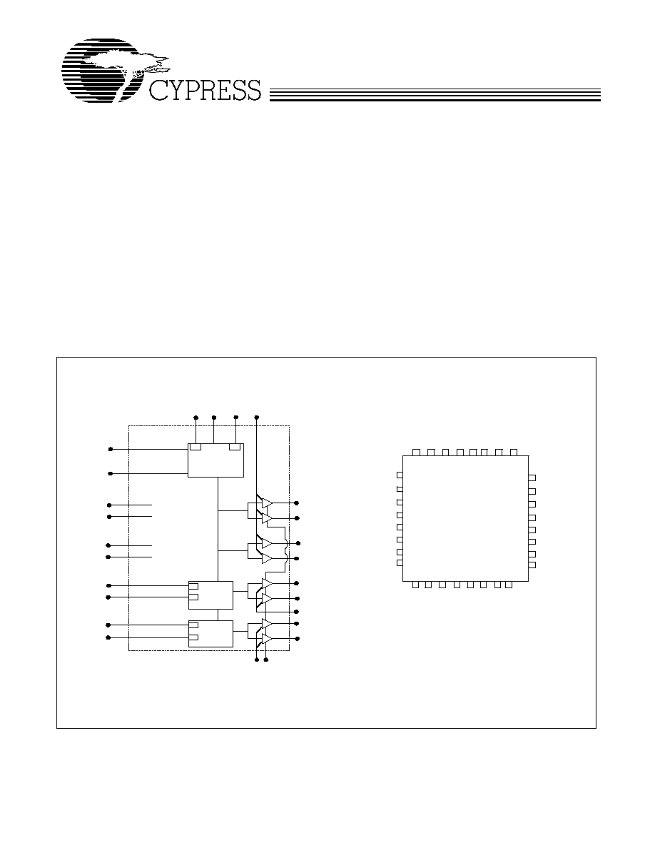
The CY2V9950 is a low-voltage, low-power, eight-output,
200-MHz clock driver. It features functions necessary to
optimize the timing of high performance computer and
communication systems.
The user can program the output banks through 3F[0:1] and
4F[0:1]pins. Any one of the outputs can be connected to
feedback input to achieve different reference frequency multi-
plication and divide ratios and zero input-output delay.
The device also features split output bank power supplies
which enable the user to run two banks (1Qn and 2Qn) at a
power supply level different from that of the other two banks
(3Qn and 4Qn). Additionally, the PE pin controls the synchro-
nization of the output signals to either the rising or the falling
edge of the reference clock.
Block Diagram
Pin Configuration
3F
0
FS
VD
D
RE
F
VSS
T
EST
2F
1
2F
0
CY2V9950
32 31 30 29 28 27 26 25
9 10 11 12 13 14 15 16
24
23
22
21
20
19
18
17
1
2
3
4
5
6
7
8
1F1
1F0
sOE#
VDDQ1
1Q0
1Q1
VSS
VSS
3F1
4F0
4F1
PE
VDDQ4
4Q0
VSS
4Q1
VSS
3Q
1
3Q
0
VD
D
Q
3
2Q
1
FB
VD
D
2Q
0
PE
TES T
FS
3
3
REF
FB
2F1:0
1F1:0
3F1:0
4F1:0
1Q 0
1Q 1
2Q 0
2Q 1
3Q 0
3Q 1
4Q 0
4Q 1
P LL
3
3
3
3
/ K
sO E #
VDDQ 1
V D D Q 4
/ M
V D D Q 3
CY2V9950
Document #: 38-07436 Rev. **
Page 2 of 9
Device Configuration
The outputs of the CY2V9950 can be configured to run at
frequencies ranging from 6 to 200 MHz. Banks 3 and 4 output
dividers are controlled by 3F[1:0] and 4F[1:0] as indicated in
Table 1 and 2 respectively.
The divider settings, output frequencies, and possible config-
urations of connecting FB to ANY output are summarized in
Table 3.
The 3-level FS control pin setting determines the nominal
operating frequency range of the divide-by-one outputs of the
device. The CY2V9950 PLL operating frequency range that
corresponds to each FS level is given in Table 4.
Notes:
1.
`PD' indicates an internal pull-down and `PU' indicates an internal pull-up. `3' indicates a three-level input buffer.
2.
A bypass capacitor (0.1
µ
F) should be placed as close as possible to each positive power pin (<0.2"). If these bypass capacitors are not close to the pins their
high frequency filtering characteristic will be cancelled by the lead inductance of the traces.
3.
When TEST = MID and sOE# = HIGH, PLL remains active with nF[1:0] = LL functioning as an output disable control for individual output banks. Skew selections
remain in effect unless nF[1:0] = LL.
4.
LL disables outputs if TEST = MID and sOE# = HIGH.
5.
When 4Q[0:1] are set to run inverted (HH mode), sOE# disables these outputs HIGH when PE = HIGH, sOE# disables them LOW when PE = LOW.
6.
These outputs are undivided copies of the VCO clock. Therefore, the formulas in this column can be used to calculate the VCO operating frequency at a given
reference frequency (F
REF
) and divider and feedback configurations. The user must select a configuration and a reference frequency that will generate a VCO
frequency that is within the range specified by FS pin. Refer to Table 4.
Pin Description
Pin
Name
I/O
[1]
Type
Description
29
REF
I
LVTTL/LVCMOS
Reference Clock Input.
13
FB
I
LVTTL
Feedback Input.
27
TEST
I
3-Level
When MID or HIGH, disables PLL (except for conditions of note 3). REF
goes to all outputs. Set LOW for normal operation.
22
sOE#
I, PD
2-Level
Synchronous Output Enable. When HIGH, it stops clock outputs (except
2Q0 and 2Q1) in a LOW state (for PE = H or M) ≠ 2Q0 and 2Q1 may be
used as the feedback signal to maintain phase lock. When TEST is held at
MID level and sOE# is high, the nF[1:0] pins act as output disable controls
for individual banks when nF[1:0] = LL. Set sOE# LOW for normal operation.
4
PE
I, PU
LVTTL
Selects Positive or Negative Edge Control and High or Low output
drive strength. When LOW / HIGH the outputs are synchronized with the
negative/positive edge of the reference clock. Please see Table 5.
24, 23, 26,
25, 1, 32, 3, 2
nF[1:0]
I
3-Level
Select frequency of the outputs. Please see Tables 1 and 2.
31
FS
I
3-Level
Selects VCO operating frequency range. Please see Table 4.
19, 20, 15,
16,10,11, 6, 7
nQ[1:0]
O
LVTTL
Four banks of two outputs. Please see Tables 1 and 2 for frequency
settings.
21
VDDQ1
[2]
PWR
Power
Power supply for Bank 1 and Bank 2 output buffers. Please see Table 6
for supply level constraints
12 VDDQ3
[2]
PWR
Power
Power supply for Bank 3 output buffers. Please see Table 6 for supply
level constraints
5
VDDQ4
[2]
PWR
Power
Power supply for Bank 4 output buffers. Please see Table 6 for supply
level constraints
14,30
VDD
[2]
PWR
Power
Power supply for internal circuitry. Please see Table 6 for supply level
constraints
8, 9, 17, 18,
28
VSS
PWR
Power
Ground.
Table 1. Output Divider Settings ≠ Bank 3
3F[1:0]
K ≠ Bank3 Output Divider
LL
[4]
2
HH
4
Other
1
Table 2. Output Divider Settings ≠ Bank 4
4F[1:0]
M ≠ Bank4 Output Divider
LL
[4]
2
HH
Inverted
[5]
Other
1
Table 3. Output Frequency Settings
Configuration
Output Frequency
FB to
1Q, 2Q
[6]
3Q
4Q
1Qn, 2Qn
F
REF
(1/K) x F
REF
(1/M) x F
REF
3Qn
K x F
REF
F
REF
(K/M) x F
REF
4Qn
M x F
REF
(M/K) x F
REF
F
REF
CY2V9950
Document #: 38-07436 Rev. **
Page 3 of 9
The PE pin determines whether the outputs synchronize to the
rising edge or the falling edge of the reference signal, as
indicated in Table 5.
The CY2V9950 features split power supply buses for Banks 1
and 2, Bank 3 and Bank 4, which enables the user to obtain
both 3.3V and 2.5V output signals from one device. The core
power supply (VDD) must be set a level which is equal or
higher than that on any one of the output power supplies.
Governing Agencies
The following agencies provide specifications that apply to the
CY2V9950. The agency name and relevant specification is
listed below.
Table 4. Frequency Range Select
FS
PLL Frequency Range
L
24 to 50 MHz
M
48 to 100 MHz
H
96 to 200 MHz
Table 5. PE Settings
PE
Synchronization
L
Negative
H
Positive
Table 6. Power Supply Constraints
VDD
VDDQ1
[7]
VDDQ3
[7]
VDDQ4
[7]
3.3V
3.3V or 2.5V
3.3V or 2.5V
3.3V or 2.5V
2.5V
2.5V
2.5V
2.5V
Agency Name
Specification
JEDEC
JESD 51 (Theta JA)
JESD 65 (Skew, Jitter)
IEEE
1596.3 (Jiter Specs)
UL-194_V0
94 (Moisture Grading)
MIL
883E Method 1012.1 (Therma Theta JC)
Absolute Maximum Conditions
Parameter
Description
Condition
Min.
Max.
Unit
V
DD
Operating Voltage
Functional @ 2.5V ± 5%
2.25
2.75
V
V
DD
Operating Voltage
Functional @ 3.3V ± 10%
2.97
3.63
V
V
IN(MIN)
Input Voltage
Relative to V
SS
V
SS
≠ 0.3
≠
V
V
IN(MAX)
Input Voltage
Relative to V
DD
≠
V
DD
+ 0.3
V
T
S
Temperature, Storage
Non Functional
≠65
+150
∞C
T
A
Temperature, Operating Ambient
Functional
≠40
+85
∞C
T
J
Temperature, Junction
Functional
≠
155
∞C
ESD
HBM
ESD Protection (Human Body Model)
MIL-STD-883, Method 3015
2000
≠
V
ÿ
JC
Dissipation, Junction to Case
Mil-Spec 883E Method 1012.1
42
∞C/W
ÿ
JA
Dissipation, Junction to Ambient
JEDEC (JESD 51)
105
∞C/W
UL-94
Flammability Rating
@1/8 in.
V ≠ 0
MSL
Moisture Sensitivity Level
1
F
IT
Failure in Time
Manufacturing Testing
10
ppm
DC Electrical Specifications @ 2.5V
Parameter
Description
Conditions
Min.
Max.
Unit
V
DD
2.5 Operating Voltage
2.5V ± 5%
2.375
2.625
V
V
IL
Input LOW Voltage
REF, FB, PE, and sOE# Inputs
≠
0.7
V
V
IH
Input HIGH Voltage
1.7
≠
V
V
IHH
[8]
Input HIGH Voltage
3-Level Inputs
(TEST, FS, nF[1:0])
(These pins are normally wired to
VDD,GND or unconnected)
V
DD
≠ ≠0.4
≠
V
V
IMM
[8]
Input MID Voltage
V
DD
/2≠0.2 V
DD
/2 + 0.2
V
V
ILL
[8]
Input LOW Voltage
≠
0.4
V
I
IL
Input Leakage Current
V
IN
= V
DD
/G
ND
,V
DD
= Max
(REF, PE, and FB inputs)
≠5
5
µ
A
Notes:
7.
VDDQ1/3/4 must not be set at a level higher than that of VDD. They can be set at different levels from each other, e.g., VDD = 3.3V, VDDQ1 = 3.3V, VDDQ3
= 2.5V and VDDQ4 = 2.5V.
8.
These Inputs are normally wired to VDD, GND or unconnected. Internal termination resistors bias unconnected inputs to VDD/2.
CY2V9950
Document #: 38-07436 Rev. **
Page 4 of 9
I
3
3-Level Input DC Current
HIGH, V
IN
= V
DD
3-Level
Inputs
(TEST, FS,
nF[1:0])
≠
200
µ
A
MID, V
IN
= V
DD
/2
≠50
50
µ
A
LOW, V
IN
= V
SS
≠200
≠
µ
A
I
PU
Input Pull-up Current
V
IN
= V
SS
, V
DD
= Max
≠25
≠
µ
A
I
PD
Input Pull-down Current
V
IN
= V
DD
, V
DD
= Max, (sOE#)
≠
100
µ
A
V
OL
Output LOW Voltage
I
OL
= 12 mA (nQ[0:1])
≠
0.4
V
V
OH
Output HIGH Voltage
I
OH
= ≠12 mA (nQ[0:1])
2.0
≠
V
I
DDQ
Quiescent Supply Current
VDD = Max, TEST = MID, REF =
LOW, sOE# = LOW, Outputs not
loaded
≠
2
mA
I
DD
Dynamic Supply Current
@100 MHz
150
mA
C
IN
Input Pin Capacitance
4
pF
DC Electrical Specifications @ 3.3V
Parameter
Description
Condition
Min.
Max.
Unit
V
DD
3.3 Operating Voltage
3.3V ± 10%
2.97
3.63
V
V
IL
Input LOW Voltage
REF, FB, PE, and sOE# Inputs
≠
0.8
V
V
IH
Input HIGH Voltage
2.0
≠
V
V
IHH
[8]
Input HIGH Voltage
3-Level Inputs
(TEST, FS, nF[1:0])
(These pins are normally wired to
VDD,GND or unconected)
V
DD
≠ ≠0.6
≠
V
V
IMM
[8]
Input MID Voltage
V
DD
/2 ≠ 0.3 V
DD
/2 + 0.3
V
V
ILL
[8]
Input LOW Voltage
≠
0.6
V
I
IL
Input Leakage Current
V
IN
= V
DD
/G
ND
,V
DD
= Max
(REF, PE, and FB inputs)
≠5
5
µ
A
I
3
3-Level Input DC Current
HIGH, V
IN
= V
DD
3-Level
Inputs
(TEST, FS,
nF[1:0])
≠
200
µ
A
MID, V
IN
= V
DD
/2
≠50
50
µ
A
LOW, V
IN
= V
SS
≠200
≠
µ
A
I
PU
Input Pull-Up Current
V
IN
= V
SS
, V
DD
= Max
≠100
≠
µ
A
I
PD
Input Pull-Down Current
V
IN
= V
DD
, V
DD
= Max, (sOE#)
≠
100
µ
A
V
OL
Output LOW Voltage
I
OL
= 12 mA, (nQ[0:1])
≠
0.4
V
V
OH
Output HIGH Voltage
I
OH
= ≠12 mA, (nQ[0:1])
2.4
≠
V
I
DDQ
Quiescent Supply Current
VDD = Max, TEST = MID, REF =
LOW, sOE# = LOW, outputs not
loaded
≠
2
mA
I
DD
Dynamic Supply Current
@100 MHz
230
mA
C
IN
Input Pin Capacitance
4
pF
AC Input Specifications
Parameter
Description
Condition
Min.
Max.
Unit
T
R
,T
F
Input Rise/Fall Time
0.8V ≠ 2.0V
≠
10
ns/V
T
PWC
Input Clock Pulse
HIGH or LOW
2
≠
ns
T
DCIN
Input Duty Cycle
10
90
%
F
REF
Reference Input Frequency
FS = LOW
6
50
MHz
FS = MID
12
100
FS = HIGH
24
200
DC Electrical Specifications @ 2.5V
(continued)
CY2V9950
Document #: 38-07436 Rev. **
Page 5 of 9
Notes:
9.
Test Load = 20 pF, terminated to VCC/2. All outputs are equally loaded.
10. t
PD
is measured at 1.5V for VDD = 3.3V and at 1.25V for VDD = 2.5V with REF rise/fall times of 0.5ns between 0.8V≠2.0V.
11. t
LOCK
is the time that is required before outputs synchronize to REF. This specification is valid with stable power supplies which are within normal operating limits.
12. Lock detector circuit may be unreliable for input frequencies lower than 4MHz, or for input signals which contain significant jitter.
Switching Characteristics
Parameter
Description
Condition
Min.
Max.
Unit
F
OR
Output frequency range
6
200
MHz
VCO
LR
VCO Lock Range
200
400
MHz
VCO
LBW
VCO Loop Bandwidth
0.25
3.5
MHz
t
SKEWPR
Matched-Pair Skew
[9]
Skew between the earliest and the latest output
transitions within the same bank
≠
150
ps
t
SKEW0
Output-Output Skew
[9]
Skew between the earliest and the latest output
transitions among all outputs
≠
200
ps
t
SKEW1
Skew between the earliest and the latest output
transitions among all same class outputs
≠
200
ps
t
SKEW2
Skew between the nominal output rising edge to the
inverted output falling edge
≠
500
ps
t
SKEW3
Skew between non-inverted outputs running at
different frequencies
≠
500
ps
t
SKEW4
Skew between nominal to inverted outputs running
at different frequencies
≠
500
ps
t
SKEW5
Skew between nominal outputs at different power
supply levels
≠
650
ps
t
PART
Part-Part Skew
Skew between the outputs of any two devices under
identical settings and conditions (VDDQ, VDD, temp,
air flow, frequency, etc.)
≠
750
ps
t
PD0
Ref to FB Propagation Delay
[10]
≠250
+250
ps
t
ODCV
Output Duty Cycle
Measured at VDD/2
45
55
%
t
PWH
Output High Time Deviation
from 50%
Measured at 2.0V for VDD = 3.3V and at 1.7V for
VDD = 2.5V.
≠
1.5
ns
t
PWL
Output Low Time Deviation
from 50%
Measured at 0.8V for VDD = 3.3V and at 0.7V for
VDD = 2.5V.
≠
2.0
ns
t
R
/t
F
Output Rise/Fall Time
Measured at 0.8V ≠ 2.0V for VDD = 3.3V and 0.7V ≠
1.7V for VDD = 2.5V
0.15
1.5
ns
t
LOCK
PLL lock time
[11,12]
≠
0.5
ms
t
CCJ
Cycle-Cycle Jitter
Divide by 1 output frequency, FS = L, FB = divide
by 1, 2, 4
≠
100
ps
Divide by 1 output frequency, FS = M/H, FB = divide
by 1, 2, 4
≠
150
ps