CPLDs at FPGA DensitiesTM
Delta39KTM ISRTM
CPLD Family
Cypress Semiconductor Corporation
∑
3901 North First Street
∑
San Jose
∑
CA 95134
∑
408-943-2600
Document #: 38-03039 Rev. *G
Revised December 9, 2002
Features
∑ High density
-- 30K to 200K usable gates
-- 512 to 3072 macrocells
-- 136 to 428 maximum I/O pins
-- Twelve dedicated inputs including four clock pins,
four global I/O control signal pins and four JTAG
interface pins for boundary scan and reconfig-
urability
∑ Embedded memory
-- 80K to 480K bits embedded SRAM
∑ 64K to 384K bits of (single-port) cluster memory
∑ 16K to 96K bits of (dual-port) channel memory
∑ High speed ≠ 233-MHz in-system operation
∑ AnyVoltTM
interface
-- 3.3V, 2.5V, and 1.8V V
CC
versions available
-- 3.3V, 2.5V,1.8V, and 1.5V I/O capability on all versions
∑ Low-power operation
-- 0.18-mm six-layer metal SRAM-based logic process
-- Full-CMOS implementation of product term array
-- Standby current as low as 1 mA at 1.8V V
CC
∑ Simple timing model
-- No penalty for using full 16 product terms/macrocell
-- No delay for single product term steering or sharing
∑ Flexible clocking
-- Spread AwareTM PLL drives all four clock networks
∑ Allows 0.6% spread spectrum input clocks
∑ Several multiply, divide and phase shift options
∑ Offered with 3.3/2.5V versions only
-- Four synchronous clock networks per device
-- Locally generated product term clock
-- Clock polarity control at each register
∑ Carry-chain logic for fast and efficient arithmetic opera-
tions
∑ Multiple I/O standards supported
-- LVCMOS (3.3/3.0/2.5/1.8V), LVTTL, 3.3V PCI, SSTL2
(I-II), SSTL3 (I-II), HSTL (I-IV), and GTL+
∑ Compatible with NOBLTM, ZBTTM, and QDRTM SRAMs
∑ Programmable slew rate control on each I/O pin
∑ User-programmable Bus Hold capability on each I/O pin
∑ Fully 3.3V PCI compliant (to 66 MHz 64-bit PCI spec, rev.
2.2)
∑ CompactPCI hot swap ready
∑ Multiple package/pinout offering across all densities
-- 208 to 676 pins in PQFP, BGA, and FBGA packages
-- Same pinout for 3.3V/2.5V and 1.8V devices
-- Simplifies design migration across density
-- Self-BootTM solution in BGA and FBGA packages
∑ In-System ReprogrammableTM (ISRTM)
-- JTAG-compliant on-board programming
-- Design changes do not cause pinout changes
∑ IEEE1149.1 JTAG boundary scan
Development Software
∑ WarpÆ
-- IEEE 1076/1164 VHDL or IEEE 1364 Verilog context
sensitive editing
-- Active-HDL FSM graphical finite state machine editor
-- Active-HDL SIM post-synthesis timing simulator
-- Architecture Explorer for detailed design analysis
-- Static Timing Analyzer for critical path analysis
-- Available on Windows 95/98/2000/XPTM and
Windows NTTM for $99
-- Supports all Cypress programmable logic products
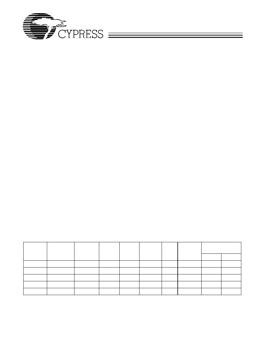
Delta39KTM ISR CPLD Family Members
Device
Typical
Gates
[1]
Macrocells
Cluster
memory
(Kbits)
Channel
memory
(Kbits)
Maximum
I/O Pins
f
MAX2
(MHz)
Speed - t
PD
Pin-to-Pin
(ns)
Standby I
CC
[2]
T
A
= 25
∞
C
3.3/2.5V
1.8V
39K30
16K ≠ 48K
512
64
16
174
233
7.2
5 mA
1 mA
39K50
23K ≠ 72K
768
96
24
218
233
7.2
5 mA
1 mA
39K100
46K ≠ 144K
1536
192
48
302
222
7.5
10 mA
2 mA
39K165
77K ≠ 241K
2560
320
80
386
181
8.5
20 mA
4 mA
39K200
92K ≠ 288K
3072
384
96
428
181
8.5
20 mA
4 mA
Notes:
1.
Upper limit of typical gates is calculated by assuming only 10% of the channel memory is used.
2.
Standby I
CC
values are with PLL not utilized, no output load and stable inputs.

Delta39KTM ISRTM
CPLD Family
Document #: 38-03039 Rev. *G
Page 2 of 91
Notes:
3.
Speed bins shown here are for commercial operating range. Please refer to Delta39K ordering information on industrial-range speed bins on page 40.
4.
Self-boot solution integrates the boot PROM (flash memory) with Delta39K die inside the same package. This flash memory can endure at least 10,000
programming/erase cycles and can retain data for at least 100 years.
Delta39K Speed Bins
[3]
Device
V
CC
233
200
181
125
83
39K30
3.3/2.5V
X
X
X
1.8V
X
X
39K50
3.3/2.5V
X
X
X
1.8V
X
X
39K100
3.3/2.5V
X
X
X
1.8V
X
X
39K165
3.3/2.5V
X
X
X
39K200
3.3/2.5V
X
X
X
1.8V
X
X
Device Package Offering and I/O Count Including Dedicated Clock and Control Inputs
Device
208 EQFP
28 ◊ 28 mm
0.5-mm pitch
256 FBGA
17 ◊ 17 mm
1.0-mm pitch
484-FBGA
23 ◊ 23 mm
1.0-mm pitch
Self-Boot
Solution
[4]
256-FBGA
17 ◊ 17 mm
1.0-mm pitch
388-BGA
35 ◊ 35 mm
1.27-mm pitch
484-FBGA
23 ◊ 23 mm
1.0-mm pitch
676-FBGA
27 ◊ 27 mm
1.0-mm pitch
39K30
136
174
174
39K50
136
180
218
218
39K100
136
180
302
294
302
39K165
136
356
294
386
39K200
136
368
294
428

Delta39KTM ISRTM
CPLD Family
Document #: 38-03039 Rev. *G
Page 3 of 91
General Description
The Delta39K family, based on a 0.18-mm, six-layer metal
CMOS logic process, offers a wide range of high-density
solutions at unparalleled system performance. The Delta39K
family is designed to combine the high speed, predictable
timing, and ease of use of CPLDs with the high densities and
low power of FPGAs. With devices ranging from 30,000 to
200,000 usable gates, the family features devices ten times
the size of previously available CPLDs. Even at these large
densities, the Delta39K family is fast enough to implement a
fully synthesizable 64-bit, 66-MHz PCI core.
The architecture is based on Logic Block Clusters (LBC) that
are connected by Horizontal and Vertical (H and V) routing
channels. Each LBC features eight individual Logic Blocks
(LB) and two cluster memory blocks. Adjacent to each LBC is
a channel memory block, which can be accessed directly from
the I/O pins. Both types of memory blocks are highly config-
urable and can be cascaded in width and depth. See Figure 1
for a block diagram of the Delta39K architecture.
4
GCLK[3:0]
4
4
4
Channel
RAM
4
GCLK[3:0]
4
4
4
4
GCLK[3:0]
4
4
4
4
4
GCLK[3:0]
PLL and Clock MUX
GCTL[3:0]
I/O Bank 6
I/O Bank 7
I/O Bank 3
I/O Bank 2
I/O
Ba
n
k
4
I/
O
B
a
n
k
5
I/
O
Ba
n
k
1
I/
O
B
a
n
k
0
LB 4
LB 3
LB 0
Cluster
RAM
LB 5
LB 6
LB 7
LB 2
LB 1
PIM
Cluster
RAM
Channel
RAM
Channel
RAM
Channel
RAM
Channel
RAM
Channel
RAM
Channel
RAM
Channel
RAM
Channel
RAM
Channel
RAM
Channel
RAM
Channel
RAM
LB 4
LB 3
LB 0
Cluster
RAM
LB 5
LB 6
LB 7
LB 2
LB 1
PIM
Cluster
RAM
LB 4
LB 3
LB 0
Cluster
RAM
LB 5
LB 6
LB 7
LB 2
LB 1
PIM
Cluster
RAM
LB 4
LB 3
LB 0
Cluster
RAM
LB 5
LB 6
LB 7
LB 2
LB 1
PIM
Cluster
RAM
LB 4
LB 3
LB 0
Cluster
RAM
LB 5
LB 6
LB 7
LB 2
LB 1
PIM
Cluster
RAM
LB 4
LB 3
LB 0
Cluster
RAM
LB 5
LB 6
LB 7
LB 2
LB 1
PIM
Cluster
RAM
LB 4
LB 3
LB 0
Cluster
RAM
LB 5
LB 6
LB 7
LB 2
LB 1
PIM
Cluster
RAM
LB 4
LB 3
LB 0
Cluster
RAM
LB 5
LB 6
LB 7
LB 2
LB 1
PIM
Cluster
RAM
LB 4
LB 3
LB 0
Cluster
RAM
LB 5
LB 6
LB 7
LB 2
LB 1
PIM
Cluster
RAM
LB 4
LB 3
LB 0
Cluster
RAM
LB 5
LB 6
LB 7
LB 2
LB 1
PIM
Cluster
RAM
LB 4
LB 3
LB 0
Cluster
RAM
LB 5
LB 6
LB 7
LB 2
LB 1
PIM
Cluster
RAM
LB 4
LB 3
LB 0
Cluster
RAM
LB 5
LB 6
LB 7
LB 2
LB 1
PIM
Cluster
RAM
Figure 1. Delta39K100 Block Diagram (Three Rows ◊ Four Columns) with I/O Bank Structure

Delta39KTM ISRTM
CPLD Family
Document #: 38-03039 Rev. *G
Page 4 of 91
All the members of the Delta39K family have Cypress's highly
regarded In-System Reprogrammability (ISR) feature, which
simplifies both design and manufacturing flows, thereby
reducing costs. The ISR feature provides the ability to recon-
figure the devices without having design changes cause
pinout or timing changes in most cases. The Cypress ISR
function is implemented through a JTAG-compliant serial
interface. Data is shifted in and out through the TDI and TDO
pins respectively. Superior routability, simple timing, and the
ISR allows users to change existing logic designs while simul-
taneously fixing pinout assignments and maintaining system
performance.
The entire family features JTAG for ISR and boundary scan,
and is compatible with the PCI Local Bus specification,
meeting the electrical and timing requirements. The Delta39K
family also features user programmable bus-hold and slew
rate control capabilities on each I/O pin.
AnyVolt Interface
All Delta39KV devices feature an on-chip regulator, which
accepts 3.3V or 2.5V on the V
CC
supply pins and steps it down
to 1.8V internally, the voltage level at which the core operates.
The Delta39KZ devices accept 1.8V on the V
CC
supply pins
directly. With Delta39K's AnyVolt technology, the I/O pins can
be connected to either 1.8V, 2.5V, or 3.3V. All Delta39K
devices are 3.3V tolerant regardless of V
CCIO
or V
CC
settings.
Global Routing Description
The routing architecture of the Delta39K is made up of
horizontal and vertical (H and V) routing channels. These
routing channels allow signals from each of the Delta39K
architectural components to communicate with one another. In
addition to the horizontal and vertical routing channels that
interconnect the I/O banks, channel memory blocks, and logic
block clusters, each LBC contains a Programmable Inter-
connect Matrix (PIMTM), which is used to route signals among
the logic blocks and the cluster memory blocks.
Figure 2 is a block diagram of the routing channels that
interface within the Delta39K architecture. The LBC is exactly
the same for every member of the Delta39K CPLD family.
Logic Block Cluster (LBC)
The Delta39K architecture consists of several logic block
clusters, each of which have eight Logic Blocks (LB) and two
cluster memory blocks connected via a Programmable Inter-
connect Matrix (PIM) as shown in Figure 3. Each cluster
memory block consists of 8-Kbit single-port RAM, which is
configurable as synchronous or asynchronous. The cluster
memory blocks can be cascaded with other cluster memory
blocks within the same LBC as well as other LBCs to
implement larger memory functions. If a cluster memory block
is not specifically utilized by the designer, Cypress's Warp
software can automatically use it to implement large blocks of
logic.
All LBCs interface with each other via horizontal and vertical
routing channels.
Note:
5.
For HSTL only.
Table 1.
Device
V
CC
V
CCIO
39KV
3.3V or 2.5V
3.3V or 2.5V or 1.8V or 1.5V
[5]
39KZ
1.8V
3.3V or 2.5V or 1.8V or 1.5V
[5]
LB
Cluster
PIM
Cluster
Memory
Block
LB
LB
LB
LB
Cluster
Memory
Block
LB
LB
LB
Channel
Memory
Block
I/O Block
I/O B
l
ock
Channel memory
outputs drive
dedicated tracks in the
horizontal and vertical
routing channels
H-to-V
PIM
V-to-H
PIM
Pin inputs from the I/O cells
drive dedicated tracks in the
horizontal and vertical routing
channels
72
72
64
64
Figure 2. Delta39K Routing Interface

Delta39KTM ISRTM
CPLD Family
Document #: 38-03039 Rev. *G
Page 5 of 91
Logic Block (LB)
The logic block is the basic building block of the Delta39K
architecture. It consists of a product term array, an intelligent
product-term allocator, and 16 macrocells.
Product Term Array
Each logic block features a 72 x 83 programmable product
term array. This array accepts 36 inputs from the PIM. These
inputs originate from device pins and macrocell feedbacks as
well as cluster memory and channel memory feedbacks.
Active LOW and active HIGH versions of each of these inputs
are generated to create the full 72-input field. The 83 product
terms in the array can be created from any of the 72 inputs.
Of the 83 product terms, 80 are for general-purpose use for
the 16 macrocells in the logic block. Two of the remaining three
product terms in the logic block are used as asynchronous set
and asynchronous reset product terms. The final product term
is the Product Term clock (PTCLK) and is shared by all 16
macrocells within a logic block.
Product Term Allocator
Through the product term allocator, Warp software automati-
cally distributes the 80 product terms as needed among the 16
macrocells in the logic block. The product term allocator
provides two important capabilities without affecting perfor-
mance: product term steering and product term sharing.
Product Term Steering
Product term steering is the process of assigning product
terms to macrocells as needed. For example, if one macrocell
requires ten product terms while another needs just three, the
product term allocator will "steer" ten product terms to one
macrocell and three to the other. On Delta39K devices,
product terms are steered on an individual basis. Any number
between 1 and 16 product terms can be steered to any
macrocell.
Product Term Sharing
Product term sharing is the process of using the same product
term among multiple macrocells. For example, if more than
one function has one or more product terms in its equation that
are common to other functions, those product terms are only
programmed once. The Delta39K product term allocator
allows sharing across groups of four macrocells in a variable
fashion. The software automatically takes advantage of this
capability so that the user does not have to intervene.
Note that neither product term sharing nor product term
steering have any effect on the speed of the product. All
steering and sharing configurations have been incorporated in
the timing specifications for the Delta39K devices.
.
Logic
Block
0
Logic
Block
1
Logic
Block
3
Logic
Block
2
Cluster
Memory
0
PIM
Logic
Block
7
Logic
Block
6
Logic
Block
4
Logic
Block
5
Cluster
Memory
1
64 Inputs From
Horizontal Routing
Channel
64 Inputs From
Vertical Routing
Channel
144 Outputs to
Horizontal and Vertical
cluster-to-channel PIMs
Clock Inputs
GCLK[3:0]
CC
CC
CC
CC
CC
CC
CC = Carry Chain
16
36
16
36
16
36
16
36
16
36
16
36
16
36
8
25
8
25
4
16
36
Figure 3. Delta39K Logic Block Cluster Diagram