Äîêóìåíòàöèÿ è îïèñàíèÿ www.docs.chipfind.ru
1
Selection Guide
6116A-20
6117A-20
6116A-25
6117A-25
6116A-35
6117A-35
6116A-45
6117A-45
6116A-55
6117A-55
Maximum Access Time (ns)
20
25
35
45
55
Maximum Operating
Commercial
100
100
100
100
80
Maximum Operating
Current (mA)
Military
125
100
100
100
Maximum Standby
Commercial
40/20
20
20
20
20
Maximum Standby
Current (mA)
Military
40
20
20
20
2K x 8 Static RAM
6116A: 11/8/89
Revision: Monday, November 8, 1993
CY6116A
CY6117A
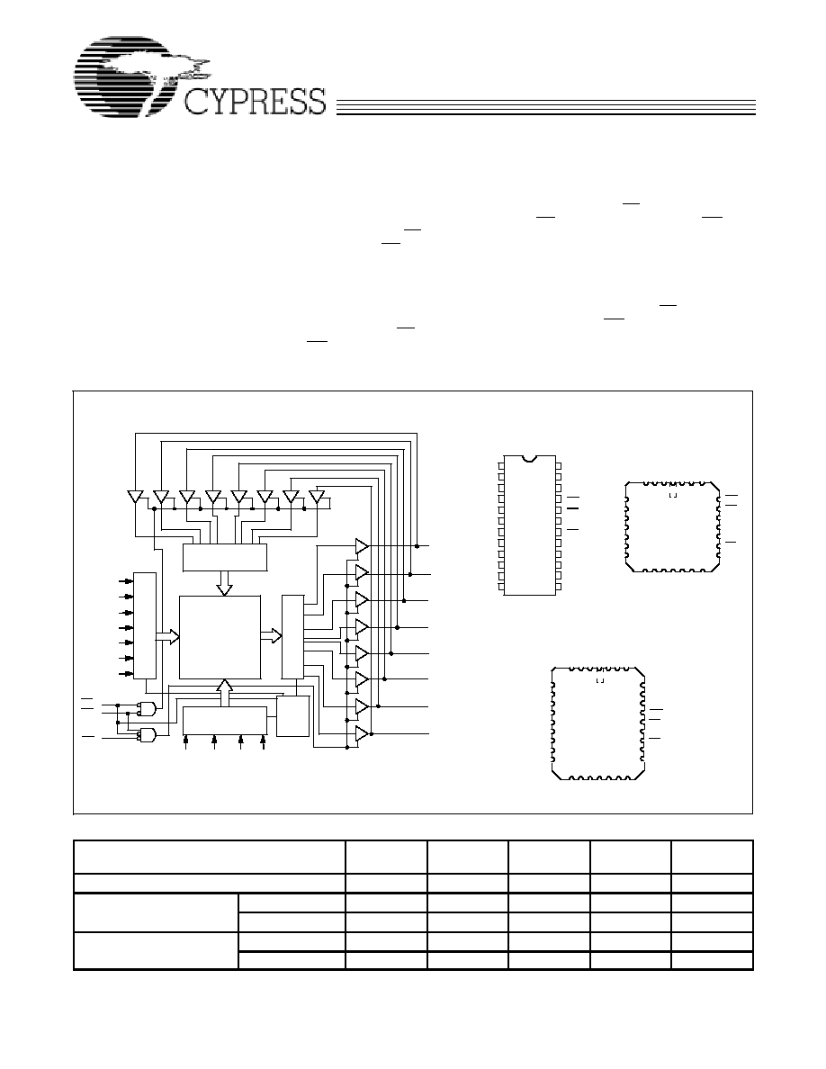
LogicBlock Diagram
Pin Configurations
Features
D
Automaticpower down when
deselected
D
CMOS for optimum speed/power
D
High speed
20 ns
D
Low active power
550 mW
D
Low standby power
110 mW
D
TTL compatible inputs and outputs
D
Capable of withstanding greater
than 2001V electrostatic discharge
Functional Description
The CY6116A and CY6117A are high
performance CMOS static RAMs orga
nized as 2048 words by 8 bits. Easy
memory expansion is provided by an active
LOW chip enable (CE) and active LOW
output enable (OE), and three state driv
ers. The CY6116A and CY6117A have an
automatic power down feature, reducing
the power consumption by 83% when de
selected.
Writingtothedeviceisaccomplishedwhen
the chip enable (CE) and write enable
(WE) inputs are both LOW. Data on the
I/Opins (I/O
0
through I/O
7
) is written into
the memory location specified on the ad
dress pins (A
0
through A
10
).
Reading the device is accomplished by tak
ing chip enable (CE) and output enable
(OE) LOW while write enable (WE) re
mains HIGH. Under these conditions, the
contents of the memory location specified
on the address pins will appear on the I/O
pins.
The I/Opins remain in high impedance
state when chip enable (CE) is HIGH or
write enable (WE) is LO W.
The CY6116A and CY6117A utilize a die
coat to insure alpha immunity.
A
1
A
2
A
4
A
5
A
6
COLUMN
DECODER
ROW
DECODER
SENSE
AMPS
INPUT BUFFER
POWER
DOWN
WE
OE
I/O
0
CE
I/O
1
I/O
2
I/O
3
1
2
3
4
5
6
7
8
9
10
11
14
15
16
20
19
18
17
21
24
23
22
Top View
DIP/SOJ
12
13
GND
A
6
A
5
A
4
A
3
A
2
A
1
A
0
WE
V
CC
A
8
A
9
A
10
I/O
7
I/O
6
I/O
5
I/O
4
A
7
I/O
0
I/O
1
I/O
2
CE
OE
I/O
3
128 x 16 x 8
ARRAY
I/O
7
I/O
6
I/O
5
I/O
4
6116A
A
0
28
4
5
6
7
8
9
10
3 2 1
27
13 14 151617
26
25
24
23
22
21
20
11
12
19
A 7 V CC
I/O
4
GND
A 6
A 5
I/O
3
I/O
2
I/O
1
6116A
CE
I/O
0
I/O
7
OE
Top View
LCC
A
3
A
7
A
8
A
9
A
10
18
I/O
5
I/O
6
A
0
A
1
NC
NC
A
3
A
2
WE
A
10
NC
NC
A 9
A 8
A 4
12
I/O
0
31
4
5
6
7
8
9
10
3 2 1
30
13
14 15 16 17
26
25
24
23
22
21
11
A 7
V CC
A
6
A
5
A
4
A
3
A
2
A
1
A
0
CE
A
9
NC
A
10
I/O
7
I/O
6
I/O
4
GND
6117A
Top View
LCC
A
8
OE
I/O
3
I/O
2
I/O
1
1819 20
27
28
29
32
NC
NC
I/O
5
NC
NC
NC
NC NC
WE
6116A-1
6116A-2
6116A-3
6116A-4
Cypress Semiconductor Corporation
D
3901 North First Street
D
San Jose
D
CA 95134
D
408-943-2600
February 1988 - Revised December 1992
CY6116A
CY6117A
6116A: 11/8/89
Revision: Monday, November 8, 1993
2
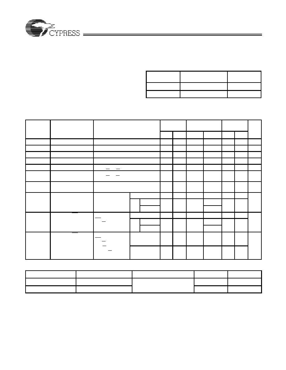
Maximum Ratings
(Above which the useful life may be impaired. For user guidelines,
not tested.)
Storage Temperature
-65
_
C to +150
_
C
. . . . . . . . . . . . . . . . . .
Ambient Temperature with
Power Applied
-55
_
C to +125
_
C
. . . . . . . . . . . . . . . . . . . . . . .
Supply Voltage to Ground Potential
(Pin 24 to Pin 12)
-0.5V to +7.0V
. . . . . . . . . . . . . . . . . . . . . . .
DC Voltage Applied to Outputs
in High Z State
-0.5V to +7.0V
. . . . . . . . . . . . . . . . . . . . . . . . .
DC Input Voltage
-3.0V to +7.0V
. . . . . . . . . . . . . . . . . . . . . . .
Output Current into Outputs (LOW)
20 mA
. . . . . . . . . . . . . .
Static Discharge Voltage
>2001V
. . . . . . . . . . . . . . . . . . . . . . .
(per MIL STD 883, Method 3015)
Latch Up Current
>200 mA
. . . . . . . . . . . . . . . . . . . . . . . . . . .
OperatingRange
Range
Ambient
Temperature
V
CC
Commercial
0
_
C to +70
_
C
5V ± 10%
Military
[1]
-55
_
C to +125
_
C
5V ± 10%
Electrical Characteristics
Over the Operating Range
[2]
6116A-20
6117A-20
6116A-25, 35, 45
6117A-25, 35, 45
6116A-55
6117A-55
Parameter
Description
Test Conditions
Min. Max.
Min.
Max.
Min. Max. Unit
V
OH
OutputHIGHVoltage V
CC
= Min., I
OH
= -4.0 mA
2.4
2.4
2.4
V
V
OL
Output LOW Voltage V
CC
= Min., I
OL
= 8.0 mA
0.4
0.4
0.4
V
V
IH
Input HIGH Voltage
2.2
V
CC
2.2
V
CC
2.2
V
CC
V
V
IL
Input LOW Voltage
[3]
-0.5
0.8
-0.5
0.8
-0.5
0.8
V
I
IX
Input Load Current
GND < V
I
< V
CC
-10 +10
-10
+10
-10 +10
mA
I
OZ
Output Leakage
Current
GND < V
I
< V
CC
,
Output Disabled
-10 +10
-10
+10
-10 +10
mA
I
OS
Output Short
Circuit Current
[4]
V
CC
= Max., V
OUT
= GND
-300
-300
-300 mA
I
CC
V
CC
Operating
S
l C
V
CC
= Max.
I
0 A
Com'l
100
100
80
mA
CC
p
g
Supply Current
CC
I
OUT
= 0 mA
f = f
MAX
= 1/t
RC
Mil 25
125
100
f = f
MAX
= 1/t
RC
35, 45
100
I
SB1
Automatic CE
P
D
C
Max. V
CC
,
CE
V
Com'l
40
20
20
mA
Power Down Current
- TTL Inputs
CC
,
CE > V
IH
f = f
MAX
Mil 25
40
20
- TTL Inputs
f = f
MAX
35, 45, 55
20
I
SB2
Automatic CE
Power Down Current
- CMOS Inputs
Max. V
CC
,
CE > V
IH
- 0.3V,
V
IN
>V
CC
- 0.3V
Com'l
20
20
20
mA
- CMOS Inputs
V
IN
>V
CC
- 0.3V
or V
IN
< 0.3V,
f = 0
Mil
20
20
Capacitance
[5]
Parameter
Description
Test Conditions
Max.
Unit
C
IN
Input Capacitance
T
A
= 25
_
C, f = 1 MHz,
V
5 0V
10
pF
C
OUT
Output Capacitance
V
CC
= 5.0V
10
pF
Notes:
1. T
A
is the instant on" case temperature.
2. See the last page of this specification for Group A subgroup testing in
formation.
3. V
IL
(min.) = -3.0V for pulse durations less than 30 ns.
4. Not more than 1 output should be shorted at one time. Duration of the
short circuit should not exceed 30 seconds.
5. Tested initially and after any design or process changes that may affect
these parameters.
CY6116A
CY6117A
6116A: 11/8/89
Revision: Monday, November 8, 1993
3
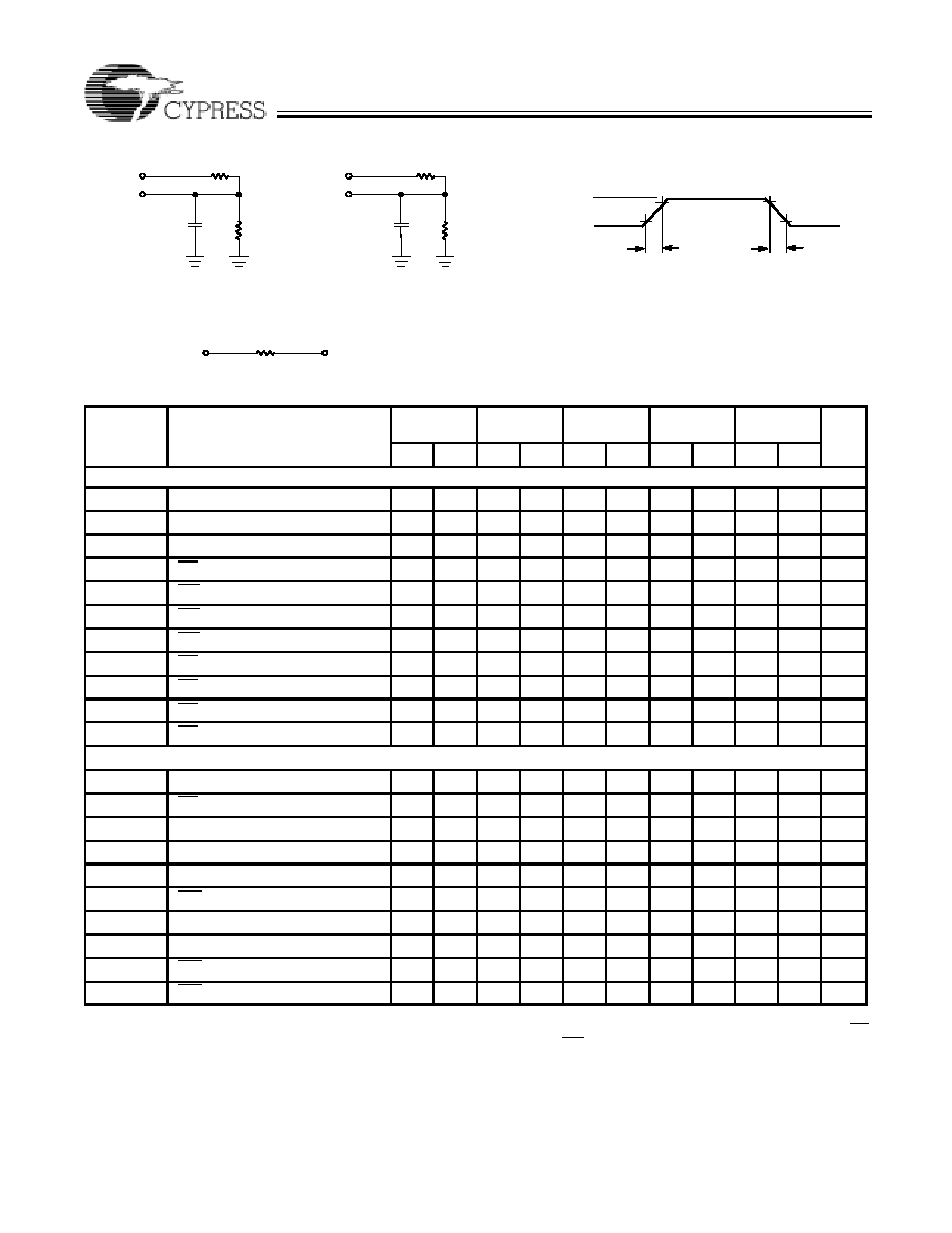
AC Test Loads and Waveforms
3.0V
5V
OUTPUT
R1 481W
R2
255W
30 pF
INCLUDING
JIG AND
SCOPE
GND
90%
10%
90%
10%
5 ns
5 ns
5V
OUTPUT
R1 481W
R2
255W
5 pF
INCLUDING
JIG AND
SCOPE
(a)
(b)
OUTPUT
1.73V
Equivalent to:
THÉVENIN EQUIVALENT
ALL INPUT PULSES
6116A-5
6116A-6
167W
Switching Characteristics
Over the Operating Range
[2, 6]
6116A-20
6117A-20
6116A-25
6117A-25
6116A-35
6117A-35
6116A-45
6117A-45
6116A-55
6117A-55
Parameter
Description
Min. Max. Min. Max. Min. Max. Min. Max. Min. Max. Unit
READ CYCLE
t
RC
Read Cycle Time
20
25
35
45
55
ns
t
AA
Address to Data Valid
20
25
35
45
55
ns
t
OHA
Data Hold from Address Change
5
5
5
5
5
ns
t
ACE
CE LOW to Data Valid
20
25
35
45
55
ns
t
DOE
OE LOW to Data Valid
10
12
15
20
25
ns
t
LZOE
OE LOW to Low Z
3
3
3
3
3
ns
t
HZOE
OE HIGH to High Z
[7]
8
10
12
15
20
ns
t
LZCE
CE LOW to Low Z
[8]
5
5
5
5
5
ns
t
HZCE
CE HIGH to High Z
[7, 8 ]
8
10
15
15
20
ns
t
PU
CE LOW to Power Up
0
0
0
0
0
ns
t
PD
CE HIGH to Power Down
20
20
20
25
25
ns
WRITE CYCLE
[9]
t
WC
Write Cycle Time
20
20
25
40
50
ns
t
SCE
CE LOW to Write End
15
20
25
30
40
ns
t
AW
Address Set Up to Write End
15
20
25
30
40
ns
t
HA
Address Hold from Write End
0
0
0
0
0
ns
t
SA
Address Set Up to Write Start
0
0
0
0
0
ns
t
PWE
WE Pulse Width
15
15
20
20
25
ns
t
SD
Data Set Up to Write End
10
10
15
15
25
ns
t
HD
Data Hold from Write End
0
0
0
0
0
ns
t
HZWE
WE LOW to High Z
7
7
10
15
20
ns
t
LZWE
WE HIGH to Low Z
5
5
5
5
5
ns
Notes:
6. Test conditions assume signal transition time of 5 ns or less, timing ref
erence levels of 1.5V, input pulse levels of 0 to 3.0V, and output loading
of the specified I
OL
/I
OH
and 30 pF load capacitance.
7. t
HZOE
, t
HZCE
, and t
HZWE
are specified with C
L
= 5 pF as in part (b)
of AC Test Loads. Transition is measured ±500 mV from steady state
voltage.
8. At any given temperature and voltage condition, t
HZCE
is less than
t
LZCE
for any given device.
9. The internal write time of the memory is defined by the overlap of CE
LOW and WE LOW. Both signals must be LOW to initiate a write and
either signal can terminate a write by going HIGH. The data input set
up and hold timing should be referenced to the rising edge of the signal
that terminates the write.
CY6116A
CY6117A
6116A: 11/8/89
Revision: Monday, November 8, 1993
4
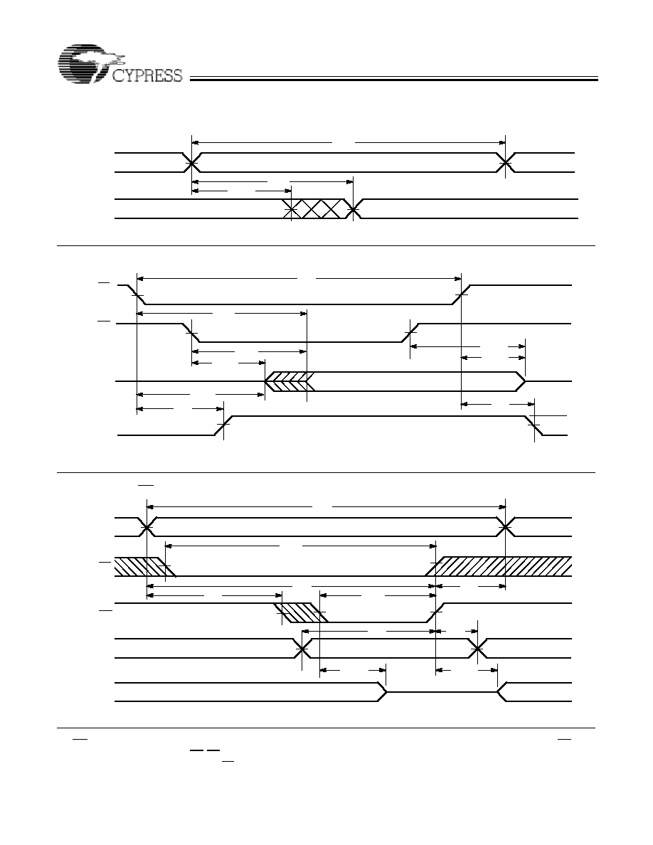
Switching Waveforms
Read Cycle No. 1
[10, 11]
ADDRESS
DATA OUT
PREVIOUS DATA VALID
DATA VALID
t
RC
t
AA
t
OHA
6116A-7
Read Cycle No. 2
[10, 12]
50%
50%
DATA VALID
t
RC
t
ACE
t
DOE
t
LZOE
t
LZCE
t
PU
DATA OUT
HIGH IMPEDANCE
IMPEDANCE
ICC
ISB
t
HZOE
t
HZCE
t
PD
OE
CE
HIGH
V
CC
SUPPLY
CURRENT
6116A-8
Write Cycle No. 1 (WE Controlled)
[9, 13]
t
WC
DATA VALID
DATA UNDEFINED
HIGH IMPEDANCE
t
SCE
t
AW
t
SA
t
PWE
t
HA
t
HD
t
HZWE
t
LZWE
t
SD
CE
WE
DATA IN
DATA I/O
ADDRESS
6116A-9
Notes:
10. WE is HIGH for read cycle.
11. Device is continuously selected. OE, CE = V
IL
.
12. Address valid prior to or coincident with CE transition LOW.
13. Data I/O pins enter high impedance state, as shown, when OE is held
LOW during write.
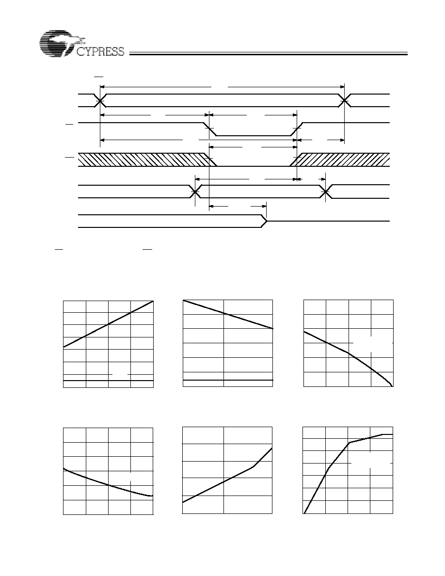
CY6116A
CY6117A
6116A: 11/8/89
Revision: Monday, November 8, 1993
5
Switching Waveforms
(continued)
Write Cycle No. 2 (CE Controlled)
[9, 13, 14]
t
WC
DATA UNDEFINED
HIGH IMPEDANCE
t
SCE
t
AW
t
SA
t
PWE
t
HA
t
HD
t
HZWE
t
SD
ADDRESS
CE
WE
DATA IN
DATA I/O
6116A-10
DATA
IN
VALID
Note:
14. If CE goes HIGH simultaneously with WE HIGH, the output remains
in a high impedance state.
Typical DC and AC Characteristics
1.2
1.4
1.0
0.6
0.4
0.2
4.0
4.5
5.0
5.5
6.0
1.6
1.4
1.2
1.0
0.8
-55
25
125
-55
25
125
1.2
1.0
0.8
NORMALIZED
t
AA
120
100
80
60
40
20
0.0
1.0
2.0
3.0
4.0
OUTPUT
SOURCE
CURRENT
(mA)
SUPPLY VOLTAGE (V)
NORMALIZED SUPPLY CURRENT
vs. SUPPLY VOLTAGE
NORMALIZED ACCESS TIME
vs. AMBIENT TEMPERATURE
AMBIENT TEMPERATURE (_C)
NORMALIZED SUPPLY CURRENT
vs. AMBIENT TEMPERATURE
AMBIENT TEMPERATURE (_C)
OUTPUT VOLTAGE (V)
OUTPUT SOURCE CURRENT
vs. OUTPUT VOLTAGE
0.0
0.8
1.4
1.3
1.2
1.1
1.0
0.9
4.0
4.5
5.0
5.5
6.0
NORMALIZED
t
AA
SUPPLY VOLTAGE (V)
NORMALIZED ACCESS TIME
vs. SUPPLY VOLTAGE
120
140
100
60
40
20
0.0
1.0
2.0
3.0
4.0
OUTPUT
SINK
CURRENT
(mA)
0
80
OUTPUT VOLTAGE (V)
OUTPUT SINK CURRENT
vs. OUTPUT VOLTAGE
0.6
0.4
0.2
0.0
NORMALIZED
I
,
I
CC
SB
NORMALIZED
I
,
I
CC
SB
I
SB
V
CC
= 5.0V
V
IN
= 5.0V
I
CC
I
CC
V
CC
= 5.0V
V
CC
= 5.0V
T
A
= 25_C
V
CC
= 5.0V
T
A
= 25_C
I
SB
T
A
= 25_C
0.6
0.8
0