ADVANCE
INFORMATION
8M (512K x 16) Static RAM
CY62157DV
MoBL
Æ
Cypress Semiconductor Corporation
∑
3901 North First Street
∑
San Jose
,
CA 95134
∑
408-943-2600
Document #: 38-05392 Rev. **
Revised May 20, 2003
Features
∑ Very high speed: 55 ns
∑ Wide voltage range: 2.20V ≠ 3.60V
∑ Pin-compatible with CY62157CV25, CY62157CV30, and
CY62157CV33
∑ Ultra-low active power
-- Typical active current: 1.5 mA @ f = 1 MHz
-- Typical active current: 12 mA @ f = f
max
∑ Ultra-low standby power
∑ Easy memory expansion with CE
1
, CE
2
, and OE
features
∑ Automatic power-down when deselected
∑ CMOS for optimum speed/power
∑ Packages offered in a 48-ball BGA, 48-pin TSOPI, and
44-pin TSOPII
Functional Description
[1]
The CY62157DV is a high-performance CMOS static RAM
organized as 512K words by 16 bits. This device features
advanced circuit design to provide ultra-low active current.
This is ideal for providing More Battery Life
(MoBL
Æ
) in
portable applications such as cellular telephones. The device
also has an automatic power-down feature that significantly
reduces power consumption by 99% when addresses are not
toggling. The device can also be put into standby mode when
deselected (CE
1
HIGH or CE
2
LOW or both BHE and BLE are
HIGH). The input/output pins (I/O
0
through I/O
15
) are placed
in a high-impedance state when: deselected (CE
1
HIGH or CE
2
LOW), outputs are disabled (OE HIGH), both Byte High
Enable and Byte Low Enable are disabled (BHE, BLE HIGH),
or during a write operation (CE
1
LOW, CE
2
HIGH and WE
LOW).
Writing to the device is accomplished by taking Chip Enables
(CE
1
LOW and CE
2
HIGH) and Write Enable (WE) input LOW.
If Byte Low Enable (BLE) is LOW, then data from I/O pins (I/O
0
through I/O
7
), is written into the location specified on the
address pins (A
0
through A
18
). If Byte High Enable (BHE) is
LOW, then data from I/O pins (I/O
8
through I/O
15
) is written into
the location specified on the address pins (A
0
through A
18
).
Reading from the device is accomplished by taking Chip
Enables (CE
1
LOW and CE
2
HIGH) and Output Enable (OE)
LOW while forcing the Write Enable (WE) HIGH. If Byte Low
Enable (BLE) is LOW, then data from the memory location
specified by the address pins will appear on I/O
0
to I/O
7
. If Byte
High Enable (BHE) is LOW, then data from memory will appear
on I/O
8
to I/O
15
. See the truth table at the back of this
datasheet for a complete description of read and write modes.
Note:
1.
For best practice recommendations, please refer to the Cypress application note entitled System Design Guidelines, which is available at http://www.cypress.com.
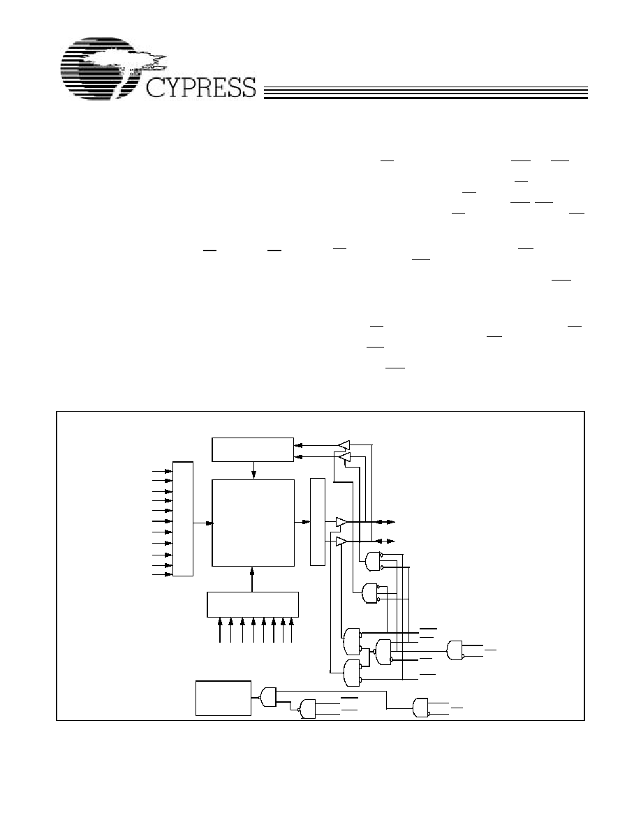
Logic Block Diagram
512K ◊ 16
RAM Array
I/O0 ≠ I/O7
ROW DECODER
A
8
A
7
A
6
A
5
A
2
COLUMN DECODER
A
11
A
12
A
13
A
14
A
15
2048 ◊ 4096
SENSE AM
PS
DATA-IN DRIVERS
OE
A
4
A
3
I/O8 ≠ I/O15
WE
BLE
BHE
A
16
A
0
A
1
A
17
A
9
A
18
A
10
Power-down
Circuit
BHE
BLE
CE
2
CE
1
CE
2
CE
1
ADVANCE
INFORMATION
CY62157DV
MoBL
Æ
Document #: 38-05392 Rev. **
Page 2 of 12
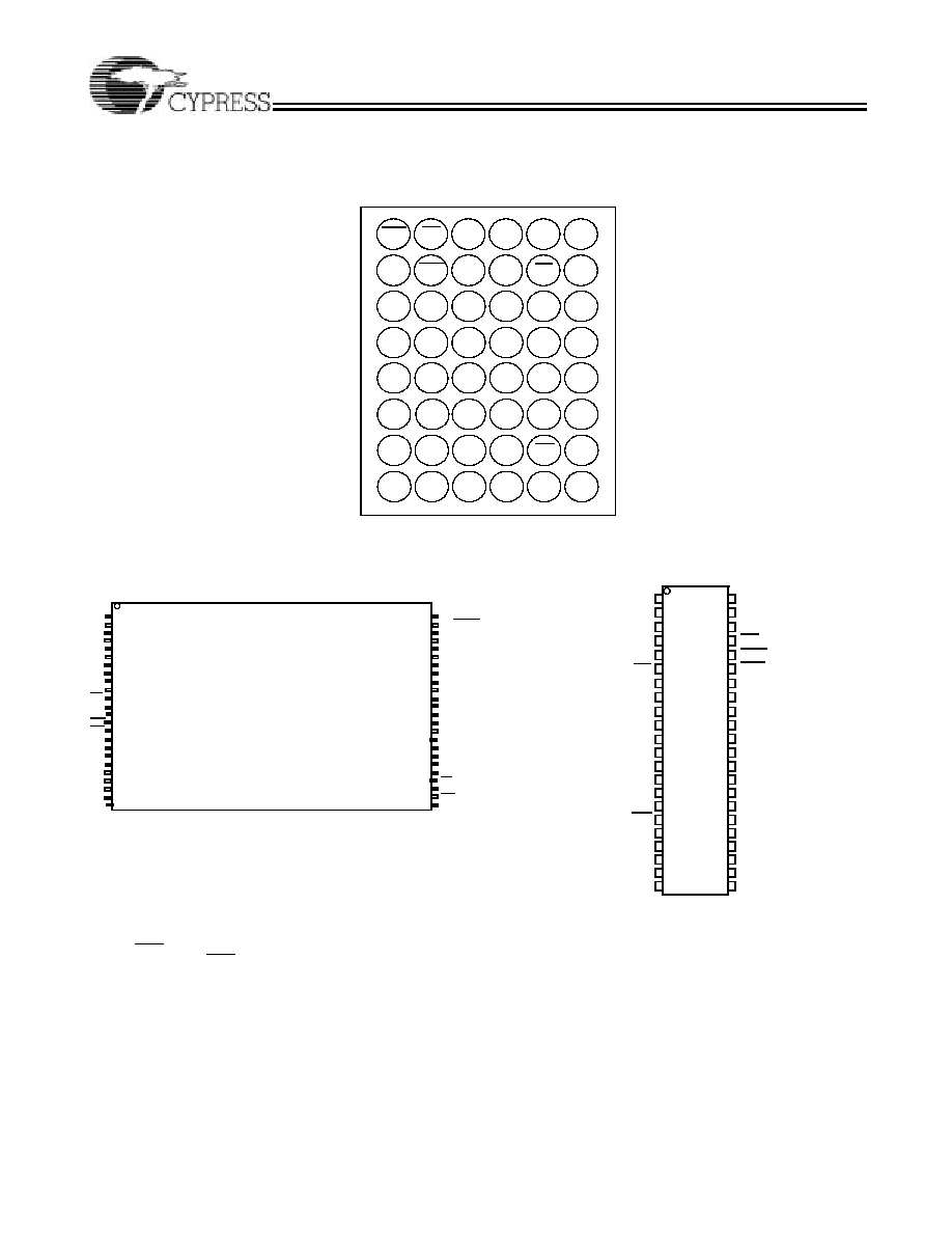
Pin Configuration
[2, 3,4]
FBGA
48TSOPI (Forward)
44 TSOP II (Forward)
Note:
2.
NC pins are not connected on the die.
3.
DNU pins have to be left floating or tied to Vss to ensure proper application.
4.
The BYTE pin in the 48-TSOPI package has to be tied to Vcc to use the device as a 512K X 16 SRAM. The 48-TSOPI package can also be used as a 1024K x 8
SRAM by tying the BYTE signal to Vss. Please refer to the data sheet entitled CY62158DV 1024K x 8 MoBL Static RAM.
WE
A
11
A
10
A
6
A
0
A
3
CE
1
I/O
10
I/O
8
I/O
9
A
4
A
5
I/O
11
I/O
13
I/O
12
I/O
14
I/O
15
V
SS
A
9
A
8
OE
Vss
A
7
I/O
0
BHE
CE
2
A
17
A
2
A
1
BLE
V
CC
I/O
2
I/O
1
I/O
3
I/O
4
I/O
5
I/O
6
I/O
7
A
15
A
14
A
13
A
12
NC
A
18
NC
3
2
6
5
4
1
D
E
B
A
C
F
G
H
Top View
A
16
DNU
Vcc
WE
1
2
3
4
5
6
7
8
9
10
11
14
31
32
36
35
34
33
37
40
39
38
12
13
41
44
43
42
16
15
29
30
V
CC
A
18
A
17
A
16
A
15
A
4
A
3
OE
V
SS
A
5
I/O
15
A
2
CE
I/O
2
I/O
0
I/O
1
BHE
A
1
A
0
18
17
20
19
I/O
3
27
28
25
26
22
21
23
24
V
SS
I/O
6
I/O
4
I/O
5
I/O
7
A
6
A
7
BLE
V
CC
I/O
14
I/O
13
I/O
12
I/O
11
I/O
10
I/O
9
I/O
8
A
9
A
10
A
11
A
12
A
14
A
13
A
8
1
2
3
4
5
6
7
8
9
10
11
12
13
14
15
16
17
18
19
20
21
22
23
24
48
47
46
45
44
43
42
41
40
39
38
37
36
35
34
33
32
31
30
29
28
27
26
25
A15
A14
A13
A12
A11
A10
A9
A8
NC
DNU
WE
CE2
DNU
BHE
BLE
A18
A17
A7
A6
A5
A4
A3
A2
A1
A16
Vcc (BYTE)
Vss
I/O15/A19
I/O7
I/O14
I/O6
I/O13
I/O5
I/O12
I/O4
Vcc
I/O11
I/O3
I/O10
I/O2
I/O9
I/O1
I/O8
I/O0
OE
Vss
CE1
A0
Top View
Top View
ADVANCE
INFORMATION
CY62157DV
MoBL
Æ
Document #: 38-05392 Rev. **
Page 3 of 12
Maximum Ratings
(Above which the useful life may be impaired. For user guide-
lines, not tested.)
Storage Temperature ................................ ≠65∞C to + 150∞C
Ambient Temperature with
Power Applied............................................ ≠55∞C to + 125∞C
Supply Voltage to Ground Potential ....≠0.2V to + V
CC
+ 0.2V
DC Voltage Applied to Outputs
in High-Z State
[5]
....................................≠0.2V to V
CC
+ 0.2V
DC Input Voltage
[5]
.................................≠0.2V to V
CC
+ 0.2V
Output Current into Outputs (LOW)............................. 20 mA
Static Discharge Voltage........................................... >2001V
(per MIL-STD-883, Method 3015)
Latch-up Current...................................................... >200 mA
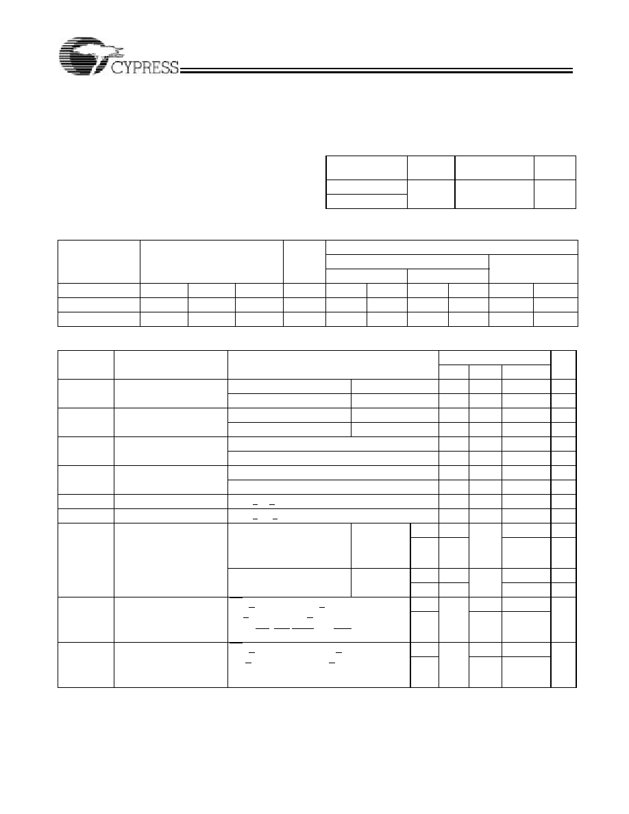
Operating Range
Device
Range
Ambient
Temperature
V
CC
[6]
CY62157DVL
Industrial
≠40∞C to +85∞C 2.20V to
3.60V
CY62157DVLL
Product Portfolio
Product
V
CC
Range (V)
Speed
(ns)
Power Dissipation
Operating I
CC
, (mA)
Standby I
SB2
, (
µ
A)
f = 1MHz
f = f
max
Min.
Typ.
[7]
Max.
Typ.
[7]
Max.
Typ.
[7]
Max.
Typ.
[7]
Max.
CY62157DVL
2.20V
3.0
3.60
55
1.5
3
12
20
2
20
CY62157DVLL
2.20V
3.0
3.60
55
1.5
3
12
15
2
8
Electrical Characteristics
Over the Operating Range
Parameter
Description
Test Conditions
CY62157DV-55
Unit
Min.
Typ.
[7]
Max.
V
OH
Output HIGH Voltage
I
OH
= ≠0.1 mA
V
CC
= 2.20V
2.0
V
I
OH
= ≠1.0 mA
V
CC
= 2.70V
2.4
V
V
OL
Output LOW Voltage
I
OL
= 0.1 mA
V
CC
= 2.20V
0.4
V
I
OL
= 2.1mA
V
CC
= 2.70V
0.4
V
V
IH
Input HIGH Voltage
V
CC
= 2.2V to 2.7V
1.8
V
CC
+ 0.3V
V
V
CC
= 2.7V to 3.6V
2.2
V
CC
+ 0.3V
V
V
IL
Input LOW Voltage
V
CC
= 2.2V to 2.7V
≠0.3
0.6
V
V
CC
= 2.7V to 3.6V
-0.3
0.8
V
I
IX
Input Leakage Current
GND < V
I
< V
CC
≠1
+1
µ
A
I
OZ
Output Leakage Current
GND < V
O
< V
CC
, Output Disabled
≠1
+1
µ
A
I
CC
V
CC
Operating Supply
Current
f = f
MAX
= 1/t
RC
V
CC
=
V
CCmax
I
OUT
= 0 mA
CMOS levels
L
12
20
mA
LL
15
mA
f = 1 MHz
L
1.5
3
mA
LL
3
mA
I
SB1
Automatic CE
Power-Down
Current -- CMOS
Inputs
CE
1
> V
CC
-
0.2V, CE
2
< 0.2V
V
IN
>V
CC
≠0.2V, V
IN
<0.2V)
f = f
MAX
(Address and Data Only),
f = 0 (OE, WE, BHE and BLE), V
CC
=3.60V
L
2
20
µ
A
LL
2
8
I
SB2
Automatic CE
Power-Down
Current -- CMOS
Inputs
CE
1
> V
CC
≠ 0.2V or CE
2
< 0.2V,
V
IN
> V
CC
≠ 0.2V or V
IN
< 0.2V,
f = 0, V
CC
= 3.60V
L
2
20
µ
A
LL
2
8
Notes:
5.
V
IL(min.)
= ≠2.0V for pulse durations less than 20 ns.
6.
Full Device AC operation requires linear Vcc ramp from 0 to Vcc(min) >= 500
µ
s.
7.
Typical values are included for reference only and are not guaranteed or tested. Typical values are measured at V
CC
= V
CC(typ.)
, T
A
= 25∞C.
ADVANCE
INFORMATION
CY62157DV
MoBL
Æ
Document #: 38-05392 Rev. **
Page 4 of 12
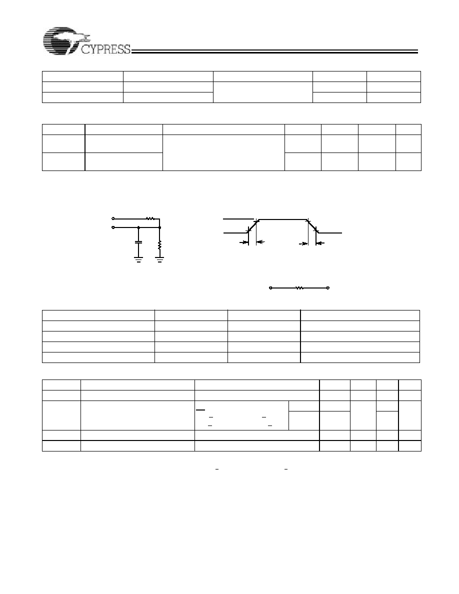
Thermal Resistance
Capacitance
[8]
Parameter
Description
Test Conditions
Max.
Unit
C
IN
Input Capacitance
T
A
= 25∞C, f = 1 MHz,
V
CC
= V
CC(typ)
6
pF
C
OUT
Output Capacitance
8
pF
Parameter
Description
Test Conditions
BGA
TSOP II
TSOP I
Unit
JA
Thermal Resistance
(Junction to Ambient)
[8]
Still Air, soldered on a 3 ◊ 4.5 inch,
two-layer printed circuit board
55
TBD
TBD
∞
C/W
JC
Thermal Resistance
(Junction to Case)
[8]
16
TBD
TBD
∞
C/W
AC Test Loads and Waveforms
Parameters
2.50V
3.0V
Unit
R1
16667
1103
R2
15385
1554
R
TH
8000
645
V
TH
1.20
1.75
V
Data Retention Characteristics
(Over the Operating Range)
Parameter
Description
Conditions
Min.
Typ.
[7]
Max.
Unit
V
DR
V
CC
for Data Retention
1.5
2.2
V
I
CCDR
Data Retention Current
V
CC
= 1.5V
CE
1
> V
CC
≠ 0.2V, CE
2
< 0.2V,
V
IN
> V
CC
≠ 0.2V or V
IN
< 0.2V
L
10
µ
A
LL
4
t
CDR
[8]
Chip Deselect to Data Retention Time
0
ns
t
R
[9]
Operation Recovery Time
t
RC
ns
Notes:
8.
Tested initially and after any design or process changes that may affect these parameters.
9.
Full device operation requires linear V
CC
ramp from V
DR
to V
CC(min.)
> 100 us or stable at V
CC(min.)
> 100 us.
V
CC
V
CC
OUTPUT
R2
50 pF
INCLUDING
JIG AND
SCOPE
GND
90%
10%
90%
10%
Rise Time = 1 V/ns
Fall Time = 1 V/ns
OUTPUT
V
Equivalent to: TH…
VENINEQUIVALENT
ALL INPUT PULSES
R
TH
R1
ADVANCE
INFORMATION
CY62157DV
MoBL
Æ
Document #: 38-05392 Rev. **
Page 5 of 12
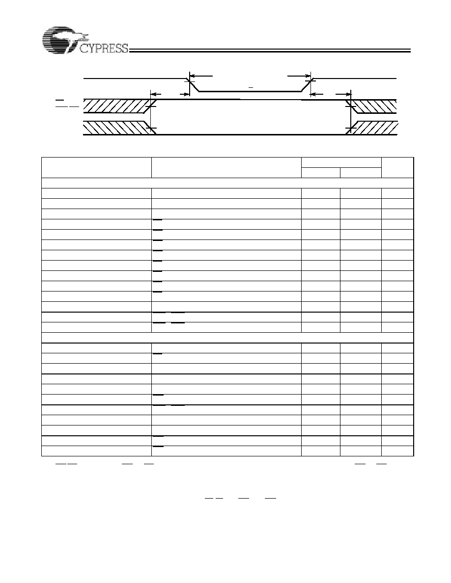
Data Retention Waveform
[10]
Switching Characteristics
Over the Operating Range
[11]
Parameter
Description
55 ns
Unit
Min.
Max.
Read Cycle
t
RC
Read Cycle Time
55
ns
t
AA
Address to Data Valid
55
ns
t
OHA
Data Hold from Address Change
10
ns
t
ACE
CE
1
LOW and CE
2
HIGH to Data Valid
55
ns
t
DOE
OE LOW to Data Valid
25
ns
t
LZOE
OE LOW to LOW Z
[12]
5
ns
t
HZOE
OE HIGH to High Z
[12, 13]
20
ns
t
LZCE
CE
1
LOW and CE
2
HIGH to Low Z
[12]
10
ns
t
HZCE
CE
1
HIGH and CE
2
LOW to High Z
[12, 13]
20
ns
t
PU
CE
1
LOW and CE
2
HIGH to Power-Up
0
ns
t
PD
CE
1
HIGH and CE
2
LOW to Power-Down
55
ns
t
DBE
BLE / BHE LOW to Data Valid
55
ns
t
LZBE
BLE / BHE LOW to Low Z
[12]
10
ns
t
HZBE
BLE / BHE HIGH to HIGH Z
[12, 13]
20
ns
Write Cycle
[14]
t
WC
Write Cycle Time
55
ns
t
SCE
CE
1
LOW and CE
2
HIGH
to Write End
40
ns
t
AW
Address Set-up to Write End
40
ns
t
HA
Address Hold from Write End
0
ns
t
SA
Address Set-up to Write Start
0
ns
t
PWE
WE Pulse Width
40
ns
t
BW
BLE / BHE LOW to Write End
40
ns
t
SD
Data Set-up to Write End
25
ns
t
HD
Data Hold from Write End
0
ns
t
HZWE
WE LOW to High-Z
[12, 13]
20
ns
t
LZWE
WE HIGH to Low-Z
[12]
10
ns
Notes:
10. BHE.BLE is the AND of both BHE and BLE. Chip can be deselected by either disabling the chip enable signals or by disabling both BHE and BLE.
11.
Test conditions for all parameters other than three-state parameters assume signal transition time of 3 ns or less, timing reference levels of V
CC(typ)
/2, input
pulse levels of 0 to V
CC(typ.)
, and output loading of the specified I
OL
/I
OH
as shown in the "AC Test Loads and Waveforms" section.
12. At any given temperature and voltage condition, t
HZCE
is less than t
LZCE
, t
HZBE
is less than t
LZBE
, t
HZOE
is less than t
LZOE
, and t
HZWE
is less than t
LZWE
for any
given device.
13. t
HZOE
, t
HZCE
, t
HZBE
, and t
HZWE
transitions are measured when the outputs enter a high-impedence state.
14. The internal Write time of the memory is defined by the overlap of WE, CE
= V
IL
, BHE and/or BLE = V
IL
, and CE
2
= V
IH
. All signals must be ACTIVE to initiate
a write and any of these signals can terminate a write by going INACTIVE. The data input set-up and hold timing should be referenced to the edge of the signal
that terminates the write.
V
CC
, min.
V
CC
, min.
t
CDR
V
DR
> 1.5 V
DATA RETENTION MODE
t
R
CE
1 or
V
CC
BHE
.
BLE
CE2
or