32Kx8 Static RAM
fax id: 1068
CY62256
Cypress Semiconductor Corporation
∑
3901 North First Street
∑
San Jose
∑
CA 95134
∑
408-943-2600
March 1996 ≠ Revised November 26, 1997
Features
∑ 4.5V≠5.5V Operation
∑ Low active power (70 ns, LL version)
-- 275 mW (max.)
∑ Low standby power (70 ns, LL version)
-- 28
µ
W (max.)
∑ 55, 70 ns access time
∑ Easy memory expansion with CE and OE features
∑ TTL-compatible inputs and outputs
∑ Automatic power-down when deselected
∑ CMOS for optimum speed/power
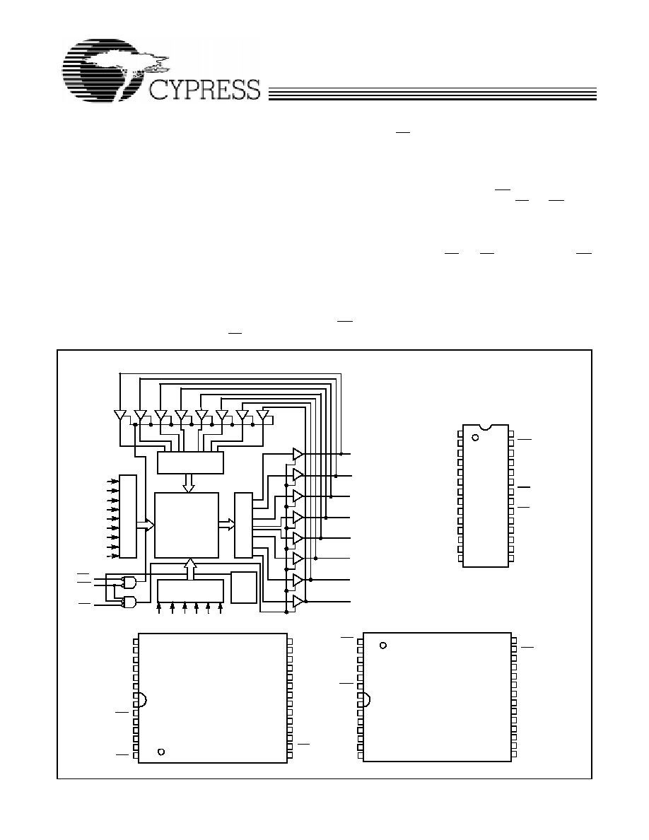
Functional Description
The CY62256 is a high-performance CMOS static RAM orga-
nized as 32,768 words by 8 bits. Easy memory expansion is
provided by an active LOW chip enable (CE) and active LOW
output enable (OE) and three-state drivers. This device has an
automatic power-down feature, reducing the power consump-
tion by 99.9% when deselected. The CY62256 is in the stan-
dard 450-mil-wide (300-mil body width) SOIC, TSOP, and
600-mil PDIP packages.
An active LOW write enable signal (WE) controls the writ-
ing/reading operation of the memory. When CE and WE inputs
are both LOW, data on the eight data input/output pins (I/O
0
through I/O
7
) is written into the memory location addressed by
the address present on the address pins (A
0
through A
14
).
Reading the device is accomplished by selecting the device
and enabling the outputs, CE and OE active LOW, while WE
remains inactive or HIGH. Under these conditions, the con-
tents of the location addressed by the information on address
pins are present on the eight data input/output pins.
The input/output pins remain in a high-impedance state unless
the chip is selected, outputs are enabled, and write enable
(WE) is HIGH.
Logic Block Diagram
Pin Configurations
A
9
A
8
A
7
A
6
A
5
A
4
A
3
A
2
COLUMN
DECODER
ROW
DE
CODER
SENSE
AM
PS
INPUTBUFFER
POWER
DOWN
WE
OE
I/O
0
CE
I/O
1
I/O
2
I/O
3
1
2
3
4
5
6
7
8
9
10
11
14
15
16
20
19
18
17
21
24
23
22
Top View
SOIC/DIP
12
13
25
28
27
26
GND
A
6
A
7
A
8
A
9
A
10
A
11
A
12
A
13
WE
V
CC
A
4
A
3
A
2
A
1
I/O
7
I/O
6
I/O
5
I/O
4
A
14
A
5
I/O
0
I/O
1
I/O
2
CE
OE
A
0
I/O
3
512x512
ARRAY
I/O
7
I/O
6
I/O
5
I/O
4
A
10
A
13
A
11
A
12
A
1
A
14
C62256≠1
C62256≠2
A
0
22
23
24
25
26
27
28
1
2
5
10
11
15
14
13
12
16
19
18
17
3
4
20
21
7
6
8
9
OE
A
1
A
2
A
3
A
4
WE
V
CC
A
5
A
6
A
7
A
8
A
9
A
0
CE
I/O
7
I/O
6
I/O
5
GND
I/O
2
I/O
1
I/O
4
I/O
0
A
14
A
10
A
11
A
13
A
12
C62256≠3
I/O
3
22
23
24
25
26
27
28
1
2
5
10
11
15
14
13
12
16
19
18
17
3
4
20
21
7
6
8
9
OE
A
1
A
2
A
3
A
4
WE
V
CC
A
5
A
6
A
7
A
8
A
9
A
0
CE
I/O
7
I/O
6
I/O
5
GND
I/O
2
I/O
1
I/O
4
I/O
0
A
14
A
10
A
11
A
13
A
12
C62256≠4
I/O
3
TSOP I
Top View
(not to scale)
TSOP I
Top View
(not to scale)
Reverse Pinout
CY62256
2
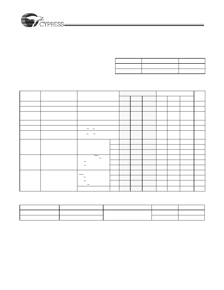
Maximum Ratings
(Above which the useful life may be impaired. For user guide-
lines, not tested.)
Storage Temperature
..................................... -
65
∞
C to +150
∞
C
Ambient Temperature with
Power Applied ................................................... 0
∞
C to +70
∞
C
Supply Voltage to Ground Potential
(Pin 28 to Pin 14)
.................................................-
0.5V to +7.0V
DC Voltage Applied to Outputs
in High Z State
[1]
....................................... -
0.5V to V
CC
+ 0.5V
DC Input Voltage
[1]
.................................... -
0.5V to V
CC
+ 0.5V
Output Current into Outputs (LOW)............................. 20 mA
Static Discharge Voltage .......................................... >2001V
(per MIL-STD-883, Method 3015)
Latch-Up Current .................................................... >200 mA
Operating Range
Range
Ambient Temperature
V
CC
Commercial
0
∞
C to +70
∞
C
5V
±
10%
Industrial
≠40
∞
C to +85
∞
C
5V
±
10%
Electrical Characteristics
Over the Operating Range
Parameter
Description
Test Conditions
CY62256
-
55
CY62256
-
70
Unit
Min.
Typ
[2]
Max.
Min.
Typ
[2]
Max.
V
OH
Output HIGH Voltage
V
CC
= Min., I
OH
=
-
1.0 mA
2.4
2.4
V
V
OL
Output LOW Voltage
V
CC
= Min., I
OL
= 2.1 mA
0.4
0.4
V
V
IH
Input HIGH Voltage
2.2
V
CC
+0.5V
2.2
V
CC
+0.5V
V
V
IL
Input LOW Voltage
-
0.5
0.8
-
0.5
0.8
V
I
IX
Input Load Current
GND < V
I
< V
CC
-
0.5
+0.5
-
0.5
+0.5
µ
A
I
OZ
Output Leakage
Current
GND < V
O
< V
CC
, Output Dis-
abled
-
0.5
+0.5
-
0.5
+0.5
µ
A
I
CC
V
CC
Operating Supply
Current
V
CC
= Max.,
I
OUT
= 0 mA,
f = f
MAX
= 1/t
RC
28
55
28
55
mA
L
25
50
25
50
mA
LL
25
50
25
50
mA
I
SB1
Automatic CE
Power-Down Current--
TTL Inputs
Max. V
CC
, CE > V
IH
,
V
IN
> V
IH
or
V
IN
< V
IL
, f = f
MAX
0.5
2
0.5
2
mA
L
0.4
0.6
0.4
0.6
mA
LL
0.3
0.5
0.3
0.5
mA
I
SB2
Automatic CE
Power-Down Current--
CMOS Inputs
Max. V
CC
,
CE > V
CC
-
0.3V
V
IN
> V
CC
-
0.3V
or V
IN
< 0.3V, f = 0
1
5
1
5
mA
L
2
50
2
50
µ
A
LL
0.1
5
0.1
5
µ
A
Indust'l Temp Range LL
0.1
10
0.1
10
µ
A
Shaded area contains preliminary information.
Capacitance
[3]
Parameter
Description
Test Conditions
Max.
Unit
C
IN
Input Capacitance
T
A
= 25
∞
C, f = 1 MHz,
V
CC
= 5.0V
6
pF
C
OUT
Output Capacitance
8
pF
Note:
1.
V
IL
(min.)
=
-
2.0V for pulse durations of less than 20 ns.
2.
Typical specifications are the mean values measured over a large sample size across normal production process variations and are taken at nominal conditions
(T
A
= 25
∞
C, V
CC
). Parameters are guaranteed by design and characterization, and not 100% tested.
3.
Tested initially and after any design or process changes that may affect these parameters.
CY62256
3
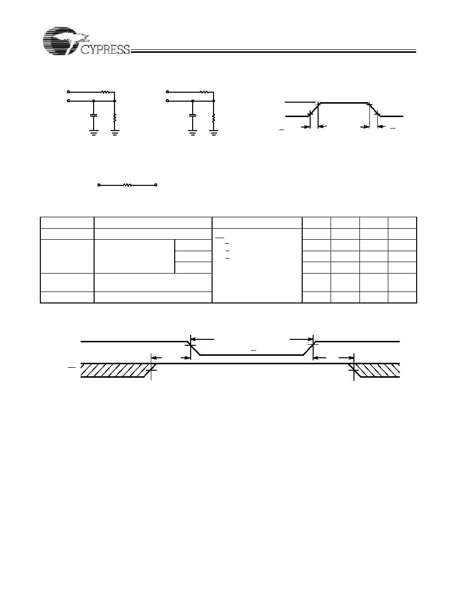
AC Test Loads and Waveforms
3.0V
5V
OUTPUT
R1 1800
R2
990
100 pF
INCLUDING
JIG AND
SCOPE
GND
90%
10%
90%
10%
< 5 ns
< 5 ns
5V
OUTPUT
R1 1800
R2
990
5 pF
INCLUDING
JIG AND
SCOPE
(a)
(b)
OUTPUT
1.77V
Equivalent to:
TH…
VENIN EQUIVALENT
ALL INPUT PULSES
C62256≠5
C62256≠6
639
Data Retention Characteristics
Parameter
Description
Conditions
[4]
Min.
Typ.
[2]
Max.
Unit
V
DR
V
CC
for Data Retention
V
CC
= 3.0V,
CE > V
CC
-
0.3V,
V
IN
> V
CC
-
0.3V or
V
IN
< 0.3V
2.0
V
I
CCDR
Data Retention Current
L
2
50
µ
A
LL
0.1
5
µ
A
LL Indust'l
0.1
10
µ
A
t
CDR
[3]
Chip Deselect to Data
Retention Time
0
ns
t
R
[3]
Operation Recovery Time
t
RC
ns
Data Retention Waveform
Note:
4.
No input may exceed V
CC
+0.5V.
C62256≠7
3.0V
3.0V
t
CDR
V
DR
> 2V
DATA RETENTION MODE
t
R
CE
V
CC
CY62256
4
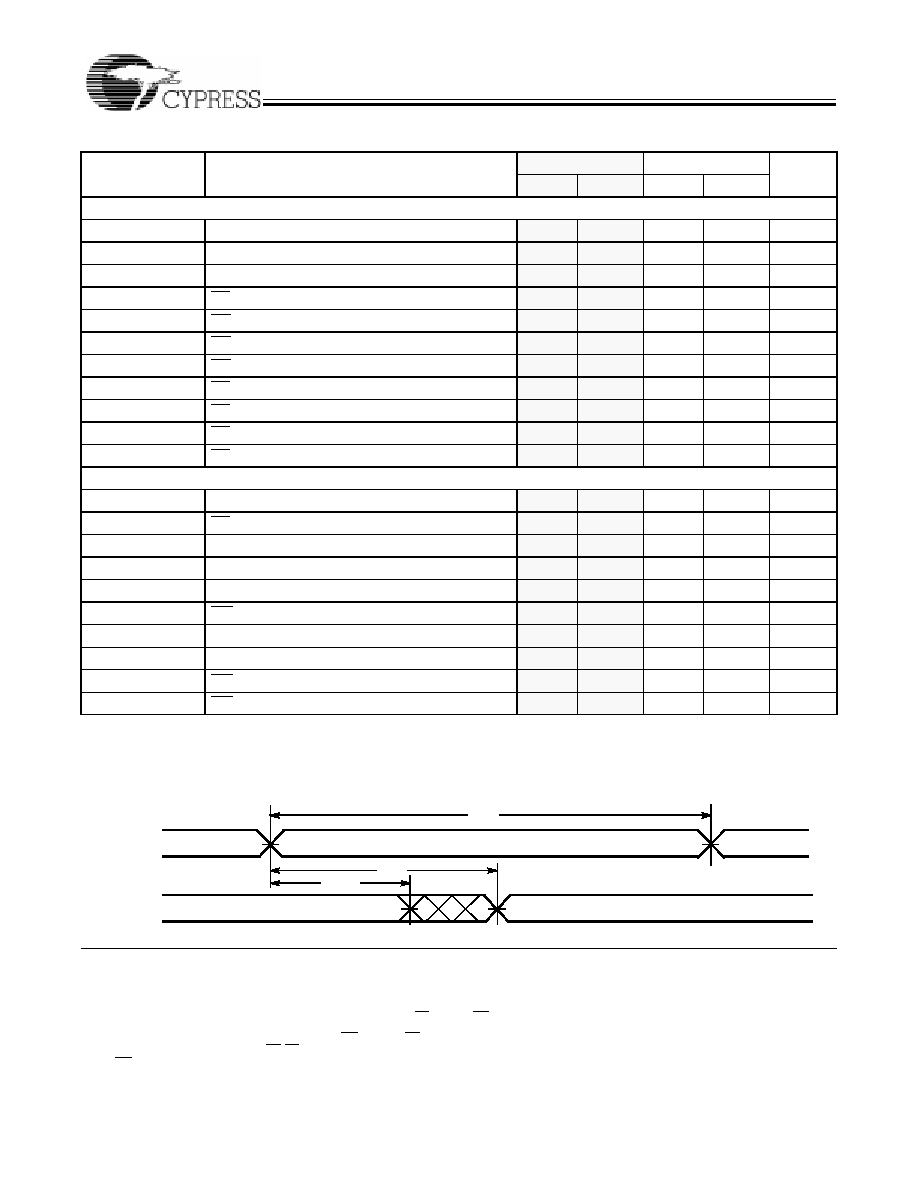
Switching Characteristics
Over the Operating Range
[5]
Parameter
Description
CY62256
-
55
CY62256
-
70
Unit
Min.
Max.
Min.
Max.
READ CYCLE
t
RC
Read Cycle Time
55
70
ns
t
AA
Address to Data Valid
55
70
ns
t
OHA
Data Hold from Address Change
5
5
ns
t
ACE
CE LOW to Data Valid
55
70
ns
t
DOE
OE LOW to Data Valid
25
35
ns
t
LZOE
OE LOW to Low Z
[6]
5
5
ns
t
HZOE
OE HIGH to High Z
[6, 7]
20
25
ns
t
LZCE
CE LOW to Low Z
[6]
5
5
ns
t
HZCE
CE HIGH to High Z
[6, 7]
20
25
ns
t
PU
CE LOW to Power-Up
0
0
ns
t
PD
CE HIGH to Power-Down
55
70
ns
WRITE CYCLE
[8, 9]
t
WC
Write Cycle Time
55
70
ns
t
SCE
CE LOW to Write End
45
60
ns
t
AW
Address Set-Up to Write End
45
60
ns
t
HA
Address Hold from Write End
0
0
ns
t
SA
Address Set-Up to Write Start
0
0
ns
t
PWE
WE Pulse Width
40
50
ns
t
SD
Data Set-Up to Write End
25
30
ns
t
HD
Data Hold from Write End
0
0
ns
t
HZWE
WE LOW to High Z
[6, 7]
20
25
ns
t
LZWE
WE HIGH to Low Z
[6]
5
5
ns
Shaded area contains preliminary information.
Switching Waveforms
Notes:
5.
Test conditions assume signal transition time of 5 ns or less, timing reference levels of 1.5V, input pulse levels of 0 to 3.0V, and output loading of the specified
I
OL
/I
OH
and 100-pF load capacitance.
6.
At any given temperature and voltage condition, t
HZCE
is less than t
LZCE
, t
HZOE
is less than t
LZOE
, and t
HZWE
is less than t
LZWE
for any given device.
7.
t
HZOE
, t
HZCE
, and t
HZWE
are specified with C
L
= 5 pF as in part (b) of AC Test Loads. Transition is measured
±
500 mV from steady-state voltage.
8.
The internal write time of the memory is defined by the overlap of CE LOW and WE LOW. Both signals must be LOW to initiate a write and either signal can terminate
a write by going HIGH. The data input set-up and hold timing should be referenced to the rising edge of the signal that terminates the write.
9.
The minimum write cycle time for write cycle #3 (WE controlled, OE LOW) is the sum of t
HZWE
and t
SD
10. Device is continuously selected. OE, CE = V
IL
.
11. WE is HIGH for read cycle.
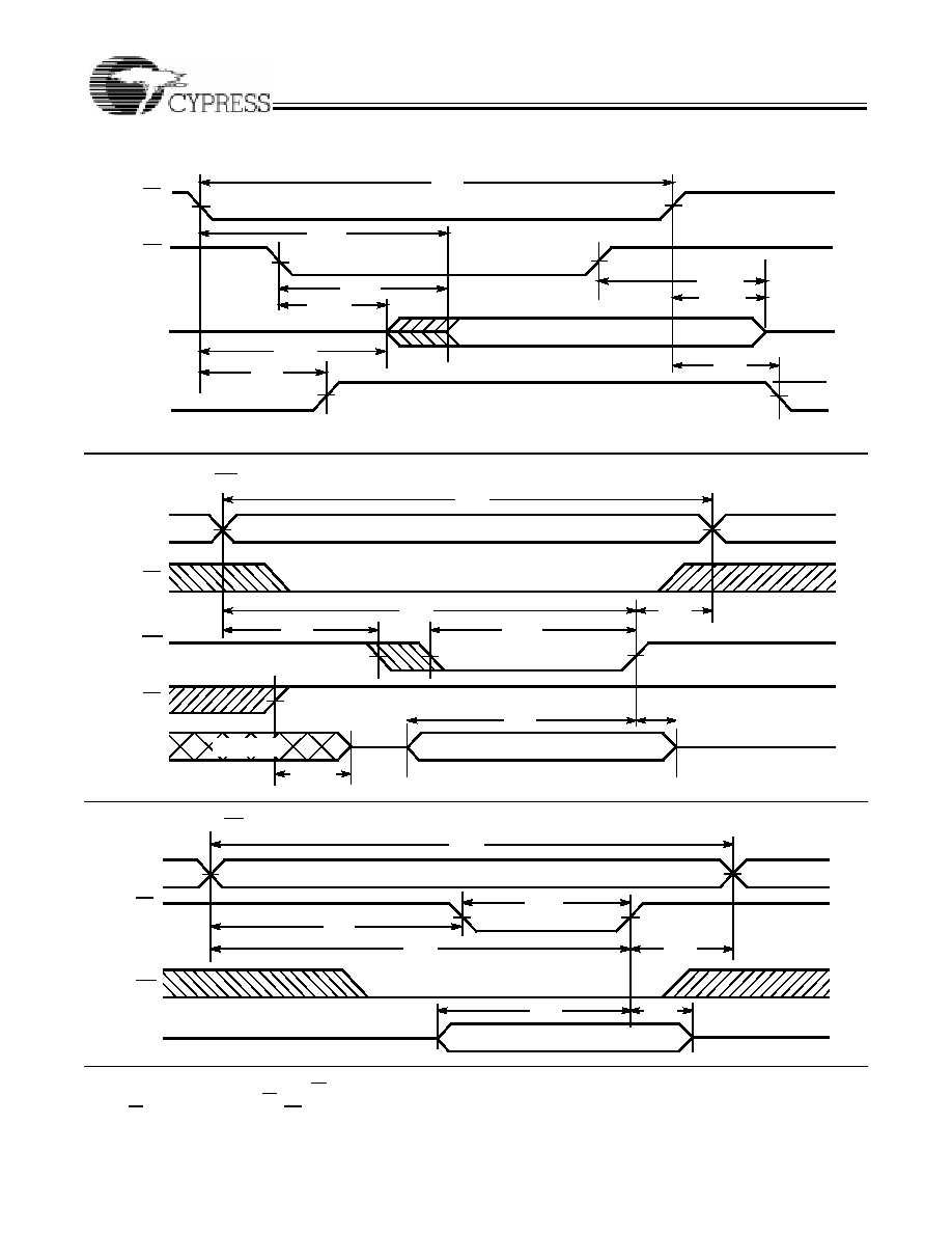
ADDRESS
DATA OUT
PREVIOUS DATA VALID
DATA VALID
t
RC
t
AA
t
OHA
C62256≠8
Read Cycle No. 1
[10,11]
CY62256
5
Notes:
12. Address valid prior to or coincident with CE transition LOW.
13. Data I/O is high impedance if OE = V
IH
.
14. If CE goes HIGH simultaneously with WE HIGH, the output remains in a high-impedance state.
Switching Waveforms
(continued)
50%
50%
DATA VALID
t
RC
t
ACE
t
DOE
t
LZOE
t
LZCE
t
PU
DATA OUT
HIGH IMPEDANCE
IMPEDANCE
ICC
ISB
t
HZOE
t
HZCE
t
PD
OE
CE
HIGH
V
CC
SUPPLY
CURRENT
C62256≠9
Read Cycle No. 2
[11,12]
t
HD
t
SD
t
PWE
t
SA
t
HA
t
AW
t
WC
DATA I/O
ADDRESS
CE
WE
OE
t
HZOE
C62256≠10
DATA
IN
VALID
NOTE
Write Cycle No. 1 (WE Controlled)
[8,13,14]
15
t
WC
t
AW
t
SA
t
HA
t
HD
t
SD
t
SCE
WE
DATA I/O
ADDRESS
CE
C62256≠11
DATA
IN
VALID
Write Cycle No. 2 (CE Controlled)
[8,13,14]

CY62256
6
Note:
15. During this period, the I/Os are in output state and input signals should not be applied.
Switching Waveforms
(continued)
DATA I/O
ADDRESS
t
HD
t
SD
t
LZWE
t
SA
t
HA
t
AW
t
WC
CE
WE
t
HZWE
C62256≠12
DATA
IN
VALID
Write Cycle No. 3 (WE Controlled, OE LOW)
[9,14]
NOTE 15
CY62256
7
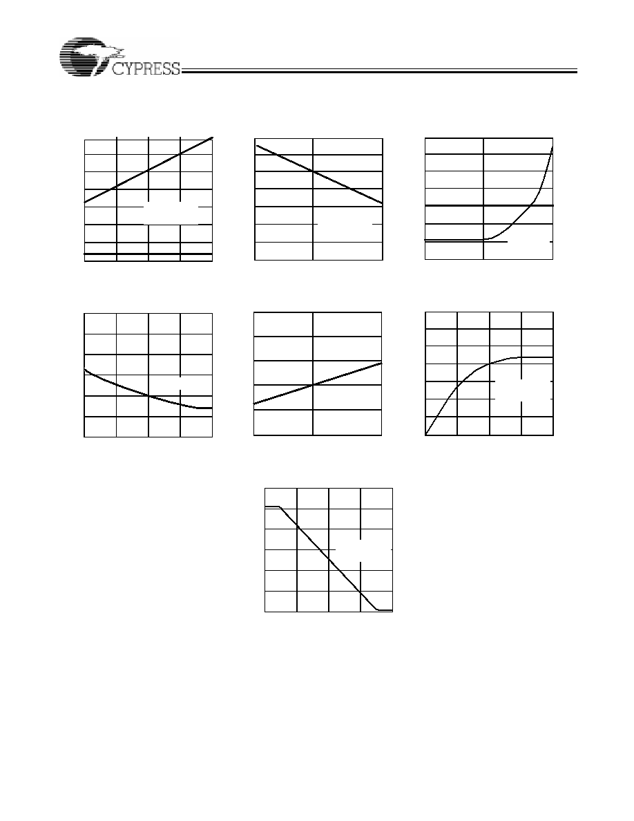
Typical DC and AC Characteristics
1.2
1.4
1.0
0.6
0.4
0.2
4.0
4.5
5.0
5.5
6.0
1.6
1.4
1.2
1.0
0.8
-
55
25
125
-
55
25
125
1.2
1.0
0.8
NORM
AL
I
Z
E
D t
AA
120
100
80
60
40
20
0.0
1.0
2.0
3.0
4.0
OUT
P
UT
SOURCE
CURRENT
(m
A)
SUPPLY VOLTAGE (V)
NORMALIZED SUPPLY CURRENT
vs. SUPPLY VOLTAGE
NORMALIZED ACCESS TIME
vs. AMBIENT TEMPERATURE
AMBIENT TEMPERATURE (
∞
C)
NORMALIZED SUPPLY CURRENT
vs. AMBIENT TEMPERATURE
AMBIENT TEMPERATURE (
∞
C)
OUTPUT VOLTAGE (V)
OUTPUT SOURCE CURRENT
vs. OUTPUT VOLTAGE
0.0
0.8
1.4
1.1
1.0
0.9
4.0
4.5
5.0
5.5
6.0
NO
RM
AL
I
Z
ED t
SUPPLY VOLTAGE (V)
NORMALIZED ACCESS TIME
vs. SUPPLY VOLTAGE
120
140
100
60
40
20
0.0
1.0
2.0
3.0
4.0
OUT
P
UT
SI
NK CURRENT
(m
A)
0
80
OUTPUT VOLTAGE (V)
OUTPUT SINK CURRENT
vs. OUTPUT VOLTAGE
0.6
0.4
0.2
0.0
N
O
R
M
A
L
IZ
ED
I
CC
N
O
R
M
AL
IZE
D
I
,
I
CC
S
B
I
CC
I
CC
V
CC
=5.0V
V
CC
=5.0V
T
A
=25
∞
C
V
CC
=5.0V
T
A
=25
∞
C
I
SB
T
A
=25
∞
C
0.6
0.8
0
AA
1.3
1.2
V
IN
=5.0V
T
A
=25
∞
C
1.4
V
CC
=5.0V
V
IN
=5.0V
-
55
25
105
2.5
2.0
1.5
CURRENT
vs. AMBIENT TEMPERATURE
AMBIENT TEMPERATURE (
∞
C)
1.0
0.5
0.0
-0.5
I
SB
3.0
STANDBY
V
CC
=5.0V
V
IN
=5.0V
I
SB
2
µ
A
CY62256
8
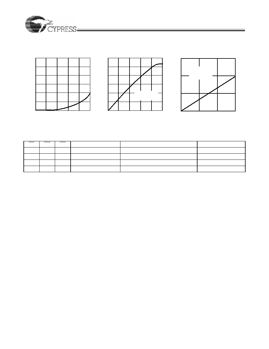
Typical DC and AC Characteristics
(continued)
3.0
2.5
2.0
1.5
1.0
0.5
0.0
1.0
2.0
3.0
4.0
N
O
R
M
A
L
IZ
ED
I
PO
SUPPLY VOLTAGE (V)
TYPICAL POWER-ON CURRENT
vs. SUPPLY VOLTAGE
30.0
25.0
20.0
15.0
10.0
5.0
0
200
400
600
800
D
E
L
T
A t
(n
s
)
AA
CAPACITANCE (pF)
TYPICAL ACCESS TIME CHANGE
vs. OUTPUT LOADING
1.25
1.00
0.75
10
20
30
40
NO
RM
AL
I
Z
ED I
CC
CYCLE FREQUENCY (MHz)
NORMALIZED I
CC
vs.CYCLE TIME
0.0
5.0
0.0
1000
0.50
V
CC
=4.5V
T
A
=25
∞
C
V
CC
=5.0V
T
A
=25
∞
C
V
IN
=0.5V
Truth Table
CE
WE
OE
Inputs/Outputs
Mode
Power
H
X
X
High Z
Deselect/Power-Down
Standby (I
SB
)
L
H
L
Data Out
Read
Active (I
CC
)
L
L
X
Data In
Write
Active (I
CC
)
L
H
H
High Z
Deselect, Output Disabled
Active (I
CC
)
CY62256
9
Shaded area contains preliminary information.
Document #: 38
-
00455
-
C
Ordering Information
Speed
(ns)
Ordering Code
Package
Name
Package Type
Operating
Range
55
CY62256
-
55SNC
S22
28-Lead 450-Mil (300-Mil Body Width) SOIC
Commercial
CY62256L
-
55SNC
S22
28-Lead 450-Mil (300-Mil Body Width) SOIC
CY62256LL
-
55SNC
S22
28-Lead 450-Mil (300-Mil Body Width) SOIC
CY62256
-
55ZRC
ZR28
28-Lead Reverse Thin Small Outline Package
CY62256L
-
55ZRC
ZR28
28-Lead Reverse Thin Small Outline Package
CY62256LL
-
55ZRC
ZR28
28-Lead Reverse Thin Small Outline Package
CY62256
-
55ZC
Z28
28-Lead Thin Small Outline Package
CY62256L
-
55ZC
Z28
28-Lead Thin Small Outline Package
CY62256LL
-
55ZC
Z28
28-Lead Thin Small Outline Package
CY62256
-
55PC
P15
28-Lead (600-Mil) Molded DIP
70
CY62256
-
70SNC
S22
28-Lead 450-Mil (300-Mil Body Width) SOIC
Commercial
CY62256L
-
70SNC
S22
28-Lead 450-Mil (300-Mil Body Width) SOIC
CY62256LL
-
70SNC
S22
28-Lead 450-Mil (300-Mil Body Width) SOIC
CY62256≠70SNI
S22
28-Lead 450-Mil (300-Mil Body Width) SOIC
Industrial
CY62256L≠70SNI
S22
28-Lead 450-Mil (300-Mil Body Width) SOIC
CY62256LL
-
70SNI
S22
28-Lead 450-Mil (300-Mil Body Width) SOIC
CY62256
-
70ZC
Z28
28-Lead Thin Small Outline Package
Commercial
CY62256L
-
70ZC
Z28
28-Lead Thin Small Outline Package
CY62256LL
-
70ZC
Z28
28-Lead Thin Small Outline Package
CY62256≠70ZI
Z28
28-Lead Thin Small Outline Package
Industrial
CY62256L
-
70ZI
Z28
28-Lead Thin Small Outline Package
CY62256LL
-
70ZI
Z28
28-Lead Thin Small Outline Package
CY62256
-
70PC
P15
28-Lead (600-Mil) Molded DIP
Commercial
CY62256L
-
70PC
P15
28-Lead (600-Mil) Molded DIP
CY62256LL
-
70PC
P15
28-Lead (600-Mil) Molded DIP
CY62256
-
70ZRC
ZR28
28-Lead Reverse Thin Small Outline Package
CY62256L
-
70ZRC
ZR28
28-Lead Reverse Thin Small Outline Package
CY62256LL
-
70ZRC
ZR28
28-Lead Reverse Thin Small Outline Package
CY62256
10
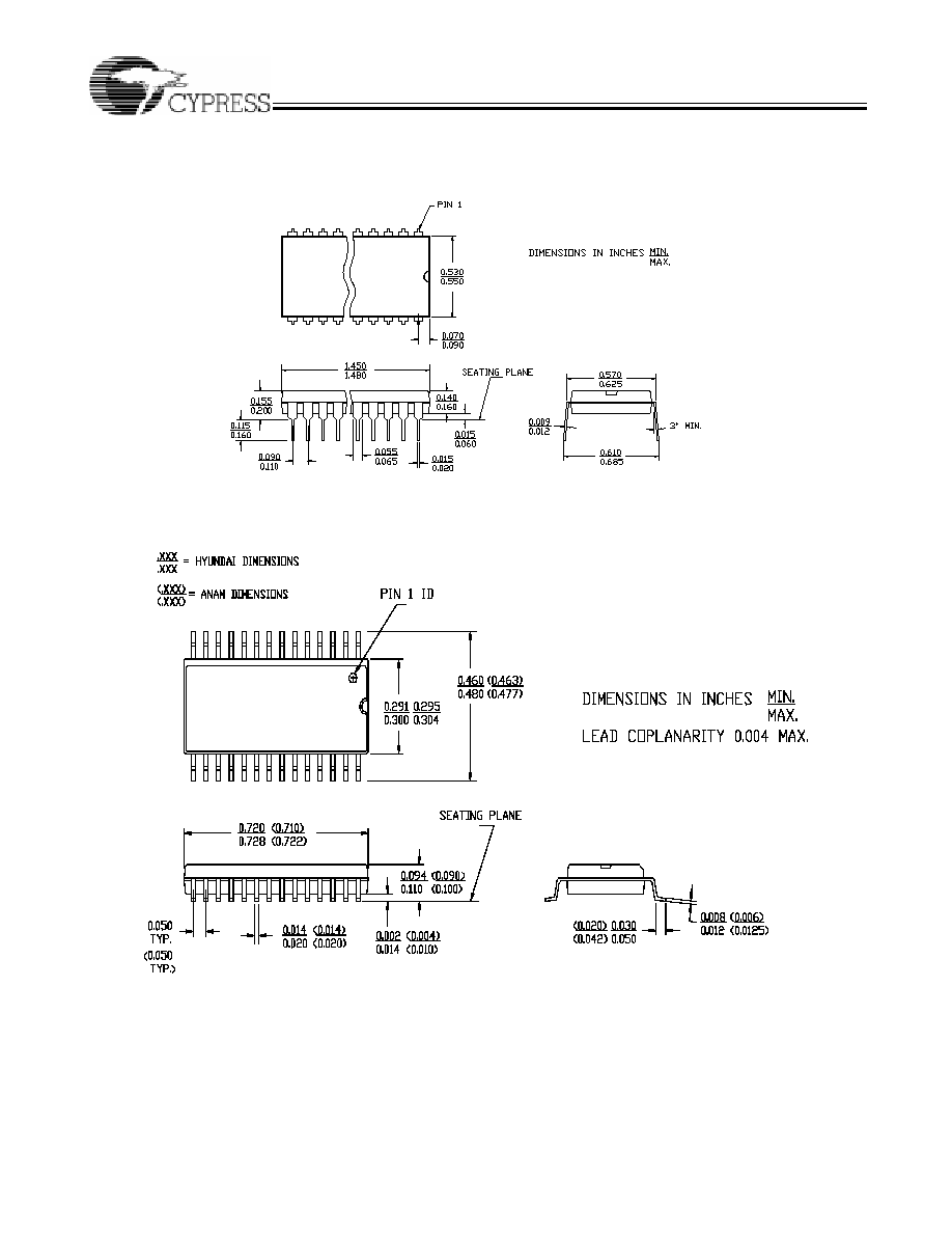
Package Diagrams
28-Lead (600-Mil) Molded DIP P15
28-Lead 450-Mil (300-Mil Body Width) SOIC S22
CY62256
11
Package Diagrams
(continued)
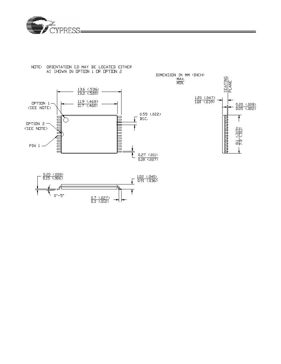
28-Lead Thin Small Outline Package Z28
CY62256
© Cypress Semiconductor Corporation, 1997. The information contained herein is subject to change without notice. Cypress Semiconductor Corporation assumes no responsibility for the use
of any circuitry other than circuitry embodied in a Cypress Semiconductor product. Nor does it convey or imply any license under patent or other rights. Cypress Semiconductor does not authorize
its products for use as critical components in life-support systems where a malfunction or failure may reasonably be expected to result in significant injury to the user. The inclusion of Cypress
Semiconductor products in life-support systems application implies that the manufacturer assumes all risk of such use and in doing so indemnifies Cypress Semiconductor against all charges.
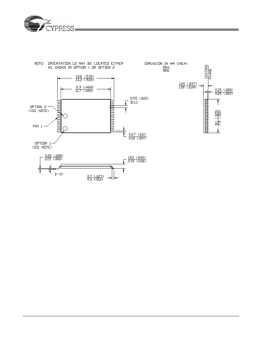
Package Diagrams
(continued)
28-Lead Reverse Thin Small Outline Package ZR28