256K (32K x 8) Static RAM
CY62256V
Cypress Semiconductor Corporation
∑
3901 North First Street
∑
San Jose
∑
CA 95134
∑
408-943-2600
Document #: 38-05057 Rev. *D
Revised June 28, 2004
Features
∑ Temperature Ranges
-- Commercial: 0∞C to 70∞C
-- Industrial: ≠40∞C to 85∞C
-- Automotive: ≠40∞C to 125∞C
∑ Speed: 70 ns and 100 ns
∑ Low voltage range:
-- CY62256V (2.7V≠3.6V)
-- CY62256V25 (2.3V≠2.7V)
∑ Low active power and standby power
∑ Easy memory expansion with CE and OE features
∑ TTL-compatible inputs and outputs
∑ Automatic power-down when deselected
∑ CMOS for optimum speed/power
∑ Package available in a standard 450-mil-wide (300-mil
body width) 28-lead narrow SOIC, 28-lead TSOP-1, and
reverse 28-lead TSOP-1 package
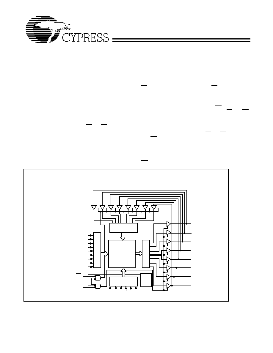
Functional Description
[1]
The CY62256V family is composed of two high-performance
CMOS static RAM's organized as 32K words by 8 bits. Easy
memory expansion is provided by an active LOW chip enable
(CE) and active LOW output enable (OE) and three-state
drivers. These devices have an automatic power-down
feature, reducing the power consumption by over 99% when
deselected.
An active LOW write enable signal (WE) controls the
writing/reading operation of the memory. When CE and WE
inputs are both LOW, data on the eight data input/output pins
(I/O
0
through I/O
7
) is written into the memory location
addressed by the address present on the address pins (A
0
through A
14
). Reading the device is accomplished by selecting
the device and enabling the outputs, CE and OE active LOW,
while WE remains inactive or HIGH. Under these conditions,
the contents of the location addressed by the information on
address pins are present on the eight data input/output pins.
The input/output pins remain in a high-impedance state unless
the chip is selected, outputs are enabled, and write enable
(WE) is HIGH.
Note:
1.
For best practice recommendations, please refer to the Cypress application note "System Design Guidelines" on http://www.cypress.com.
A
9
A
8
A
7
A
6
A
5
A
4
A
3
A
2
COLUMN
DECODER
ROW DECODER
SENSE AMPS
INPUTBUFFER
POWER
DOWN
WE
OE
I/O
0
CE
I/O
1
I/O
2
I/O
3
512 ◊ 512
ARRAY
I/O
7
I/O
6
I/O
5
I/O
4
A
10
A
13
A
11
A
12
A
A
14
A
1
0
Logic Block Diagram
CY62256V
Document #: 38-05057 Rev. *D
Page 2 of 13
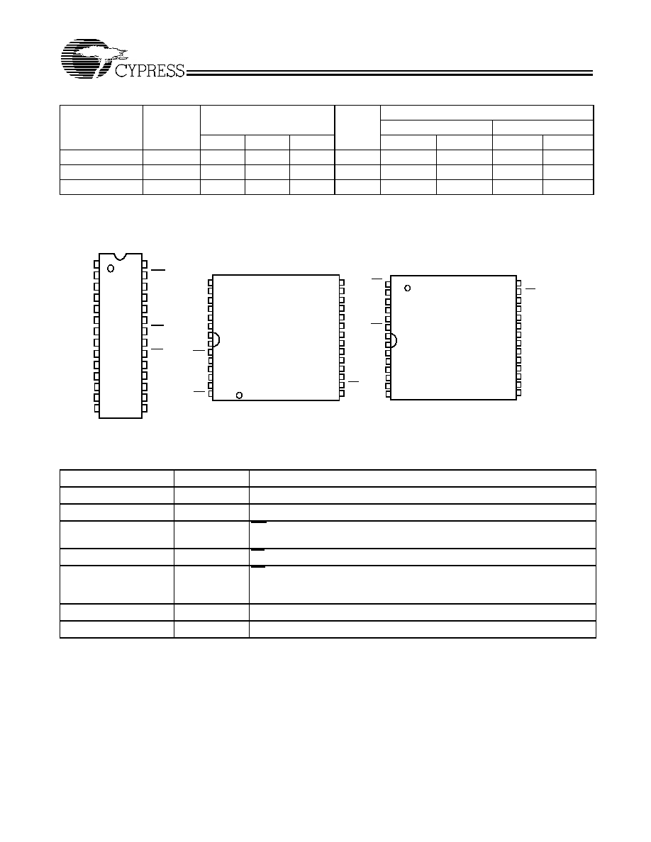
Pin Configurations
Product Portfolio
Product
V
CC
Range (V)
Speed
Power Dissipation
Operating, I
CC
(mA)
Standby, I
SB2
(
µA)
Range
Min.
Typ.
[2]
Max.
(ns)
Typ.
[2]
Max.
Typ.
[2]
Max.
CY62256VLL
Com'l / Ind'l
2.7
3.0
3.6
70
11
30
0.1
5
CY62256VLL
Automotive
2.7
3.0
3.6
70
11
30
0.1
130
CY62256V25LL
Com'l
2.3
2.5
2.7
100
9 15
0.1
4
1
2
3
4
5
6
7
8
9
10
11
14
15
16
20
19
18
17
21
24
23
22
Top View
Narrow SOIC
12
13
25
28
27
26
GND
A6
A7
A8
A9
A10
A11
A12
A13
WE
VCC
A4
A3
A2
A1
I/O7
I/O6
I/O5
I/O4
A14
A5
I/O0
I/O1
I/O2
CE
OE
A0
I/O3
22
23
24
25
26
27
28
1
2
5
10
11
15
14
13
12
16
19
18
17
3
4
20
21
7
6
8
9
OE
A
1
A
2
A
3
A
4
WE
V
CC
A
5
A
6
A
7
A
8
A
9
A
0
CE
I/O
7
I/O
6
I/O
5
GND
I/O
2
I/O
1
I/O
4
I/O
0
A
14
A
10
A
11
A
13
A
12
I/O
3
TSOP I
Top View
(not to scale)
Reverse Pinout
22
23
24
25
26
27
28
1
2
5
10
11
15
14
13
12
16
19
18
17
3
4
20
21
7
6
8
9
OE
A
1
A
2
A
3
A
4
WE
V
CC
A
5
A
6
A
7
A
8
A
9
A
0
CE
I/O
7
I/O
6
I/O
5
GND
I/O
2
I/O
1
I/O
4
I/O
0
A
14
A
10
A
11
A
13
A
12
I/O
3
TSOP I
Top View
(not to scale)
Pin Definitions
Pin Number
Type
Description
1-10, 21, 23-26
Input
A
0
-A
14
. Address Inputs
11-13, 15-19
Input/Output
I/O
0
-I/O
7
. Data lines. Used as input or output lines depending on operation
27
Input/Control
WE. When selected LOW, a WRITE is conducted. When selected HIGH, a READ
is conducted
20
Input/Control
CE. When LOW, selects the chip. When HIGH, deselects the chip
22
Input/Control
OE. Output Enable. Controls the direction of the I/O pins. When LOW, the I/O pins
behave as outputs. When deasserted HIGH, I/O pins are three-stated, and act as
input data pins
14
Ground
GND. Ground for the device
28
Power Supply
Vcc. Power supply for the device
Notes:
2.
Typical values are included for reference only and are not guaranteed or tested. Typical values are measured at V
CC
= V
CC
Typ., T
A
= 25∞C, and t
AA
= 70 ns.
CY62256V
Document #: 38-05057 Rev. *D
Page 3 of 13
Maximum Ratings
(Above which the useful life may be impaired. For user guide-
lines, not tested.)
Storage Temperature .................................≠65∞C to +150∞C
Ambient Temperature with
Power Applied.............................................≠55∞C to +125∞C
Supply Voltage to Ground Potential
(Pin 28 to Pin 14) ........................................... ≠0.5V to +4.6V
DC Voltage Applied to Outputs
in High-Z State
[3]
....................................≠0.5V to V
CC
+ 0.5V
DC Input Voltage
[3]
.................................≠0.5V to V
CC
+ 0.5V
Output Current into Outputs (LOW) .............................20 mA
Static Discharge Voltage.......................................... > 2001V
(per MIL-STD-883, Method 3015)
Latch-up Current.................................................... > 200 mA
Operating Range
Device
Range
Ambient
Temperature
(T
A
)
[4]
V
CC
CY62256V
Commercial
0
∞
C to +70
∞
C 2.7V
to
3.6V
Industrial
-40
∞
C to
+85
∞
C
Automotive
-40
∞
C to
+125
∞
C
CY62256V25
Commercial
0
∞
C to +70
∞
C 2.3V
to
2.7V
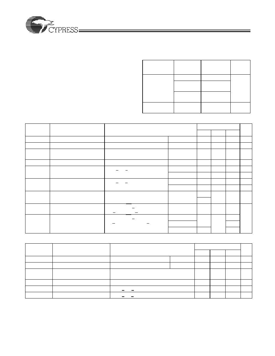
Electrical Characteristics
Over the Operating Range
Parameter
Description
Test Conditions
CY62256V-70
Unit
Min.
Typ.
[2]
Max.
V
OH
Output HIGH Voltage
I
OH
=
-1.0 mA
V
CC
= 2.7V
2.4
V
V
OL
Output LOW Voltage
I
OL
= 2.1 mA
V
CC
= 2.7V
0.4
V
V
IH
Input HIGH Voltage
2.2
V
CC
+0.3V
V
V
IL
Input Leakage Voltage
≠0.5
0.8
V
I
IX
Input Leakage Current
GND < V
IN
< V
CC
Com'l, Ind'l
≠1
+1
µA
Automotive
-10
+10
µA
I
OZ
Output Leakage Current
GND < V
IN
< V
CC
, Output Disabled Com'l, Ind'l
≠1
+1
µA
Automotive
-10
+10
µA
I
CC
V
CC
Operating Supply
Current
V
CC
= 3.6V, I
OUT
= 0 mA,
f = f
MAX
= 1/t
RC
All ranges
11
30
mA
I
SB1
Automatic CE Power-down
Current-- TTL Inputs
V
CC
= 3.6V, CE > V
IH
,
V
IN
> V
IH
or V
IN
< V
IL
, f = f
MAX
All ranges
100
300
µA
I
SB2
Automatic CE Power-down
Current-- CMOS Inputs
V
CC
= 3.6V, CE > V
CC
≠ 0.3V
V
IN
> V
CC
≠ 0.3V or V
IN
< 0.3V, f = 0
Com'l
0.1
5
Ind'l
10
Automotive
130
Electrical Characteristics
Over the Operating Range
Parameter
Description
Test Conditions
CY62256V25-100
Unit
Min.
Typ.
[2]
Max.
V
OH
Output HIGH Voltage
I
OH
=
-0.1 mA
Vcc=2.3V
2
V
V
OL
Output LOW Voltage
I
OL
= 0.1 mA
Vcc= 2.3V
0.4
V
V
IH
Input HIGH Voltage
1.7
Vcc +
0.3V
V
V
IL
Input LOW Voltage
≠0.3
0.7
V
I
IX
Input Leakage Current
GND < V
IN
< V
CC
≠1
+1
µA
I
OZ
Output Leakage Current
GND < V
IN
< V
CC
, Output Disabled
≠1
+1
µA
Notes:
3.
V
IL
(min.)
= ≠2.0V for pulse durations of less than 20 ns.
4.
T
A
is the "Instant-On" case temperature
CY62256V
Document #: 38-05057 Rev. *D
Page 4 of 13
I
CC
V
CC
Operating Supply Current V
CC
= 2.7V, I
OUT
= 0 mA, f = f
MAX
= 1/t
RC
Com'l, Ind'l
9
15
mA
I
SB1
Automatic CE Power-down
Current-- TTL Inputs
V
CC
= 2.7V, CE > V
IH
,
V
IN
> V
IH
or V
IN
< V
IL
, f = f
MAX
Com'l, Ind'l
75
225
µA
I
SB2
Automatic CE Power-down
Current -- CMOS Inputs
V
CC
= 2.7V, CE > V
CC
- 0.3V
V
IN
> V
CC
≠ 0.3V or V
IN
< 0.3V, f = 0
Com'l
0.1
4
Ind'l
8
Capacitance
[5]
Parameter
Description
Test Conditions
Max.
Unit
C
IN
Input Capacitance
T
A
= 25∞C, f = 1 MHz,
V
CC
= 3.0V
6
pF
C
OUT
Output Capacitance
8
pF
AC Test Loads and Waveforms
Parameter
3.3V
2.5V
Units
R1
1100
16600
Ohms
R2
1500
15400
Ohms
RTH
645
8000
Ohms
VTH
1.750
1.20
Volts
Notes:
5.
Tested initially and after any design or process changes that may affect these parameters.
Electrical Characteristics
Over the Operating Range (continued)
Parameter
Description
Test Conditions
CY62256V25-100
Unit
Min.
Typ.
[2]
Max.
V
CC
V
CC
OUTPUT
R2
50 pF
INCLUDING
JIG AND
SCOPE
GND
90%
10%
90%
10%
< 5 ns
< 5 ns
OUTPUT
V
th
Equivalent to:
TH… VENIN EQUIVALENT
ALL INPUT PULSES
R1
R
th
CY62256V
Document #: 38-05057 Rev. *D
Page 5 of 13
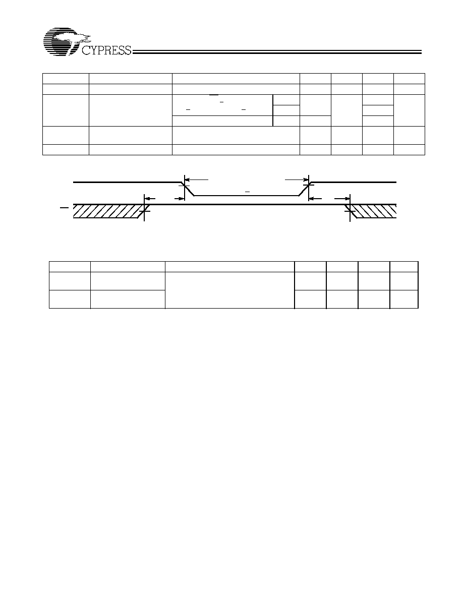
Data Retention Characteristics
(Over the Operating Range)
Parameter
Description
Conditions
[6]
Min.
Typ.
[2]
Max.
Unit
V
DR
V
CC
for Data Retention
1.4
V
I
CCDR
Data Retention Current
V
CC
= 1.6V, CE > V
CC
≠ 0.3V,
V
IN
> V
CC
≠ 0.3V or V
IN
< 0.3V
Com'l
0.1
3
µA
Ind'l
6
Auto
50
t
CDR
[6]
Chip Deselect to Data
Retention Time
0
ns
t
R
[6]
Operation Recovery Time
t
RC
ns
Data Retention Waveform
Notes:
6.
No input may exceed V
CC
+ 0.3V.
1.8V
1.8V
t
CDR
V
DR
> 1.4V
DATA RETENTION MODE
t
R
CE
V
CC
Thermal Resistance
Parameter
Description
Test Conditions
SOIC
TSOPI
RTSOPI
Unit
JA
Thermal Resistance
(Junction to Ambient)
[6]
Still Air, soldered on a 3 ◊ 4.5 inch,
four-layer printed circuit board
68.45
87.62
87.62
∞C/W
JC
Thermal Resistance
(Junction to Case)
[5]
26.94
23.73
23.73
∞C/W