7b9910.frm
Low Skew
Clock Buffer
CY7B9910
CY7B9920
Cypress Semiconductor Corporation
·
3901 North First Street
·
San Jose
·
CA 95134
·
408-943-2600
November 1994 - Revised July 7, 1997
Features
· All outputs skew <100 ps typical (250 max.)
· 15- to 80-MHz output operation
· Zero input to output delay
· 50% duty-cycle outputs
· Outputs drive 50
terminated lines
· Low operating current
· 24-pin SOIC package
· Jitter: <200 ps peak to peak, <25 ps RMS
· Compatible with PentiumTM-based processors
Functional Description
The CY7B9910 and CY7B9920 Low Skew Clock Buffers offer
low-skew system clock distribution. These multiple-output
clock drivers optimize the timing of high-performance comput-
er systems. Eight individual drivers can each drive terminated
transmission lines with impedances as low as 50
while deliv-
ering minimal and specified output skews and full-swing logic
levels (CY7B9910 TTL or CY7B9920 CMOS).
The completely integrated PLL allows "zero delay" capability.
External divide capability, combined with the internal PLL, allows
distribution of a low-frequency clock that can be multiplied by virtu-
ally any factor at the clock destination. This facility minimizes clock
distribution difficulty while allowing maximum system clock speed
and flexibility.
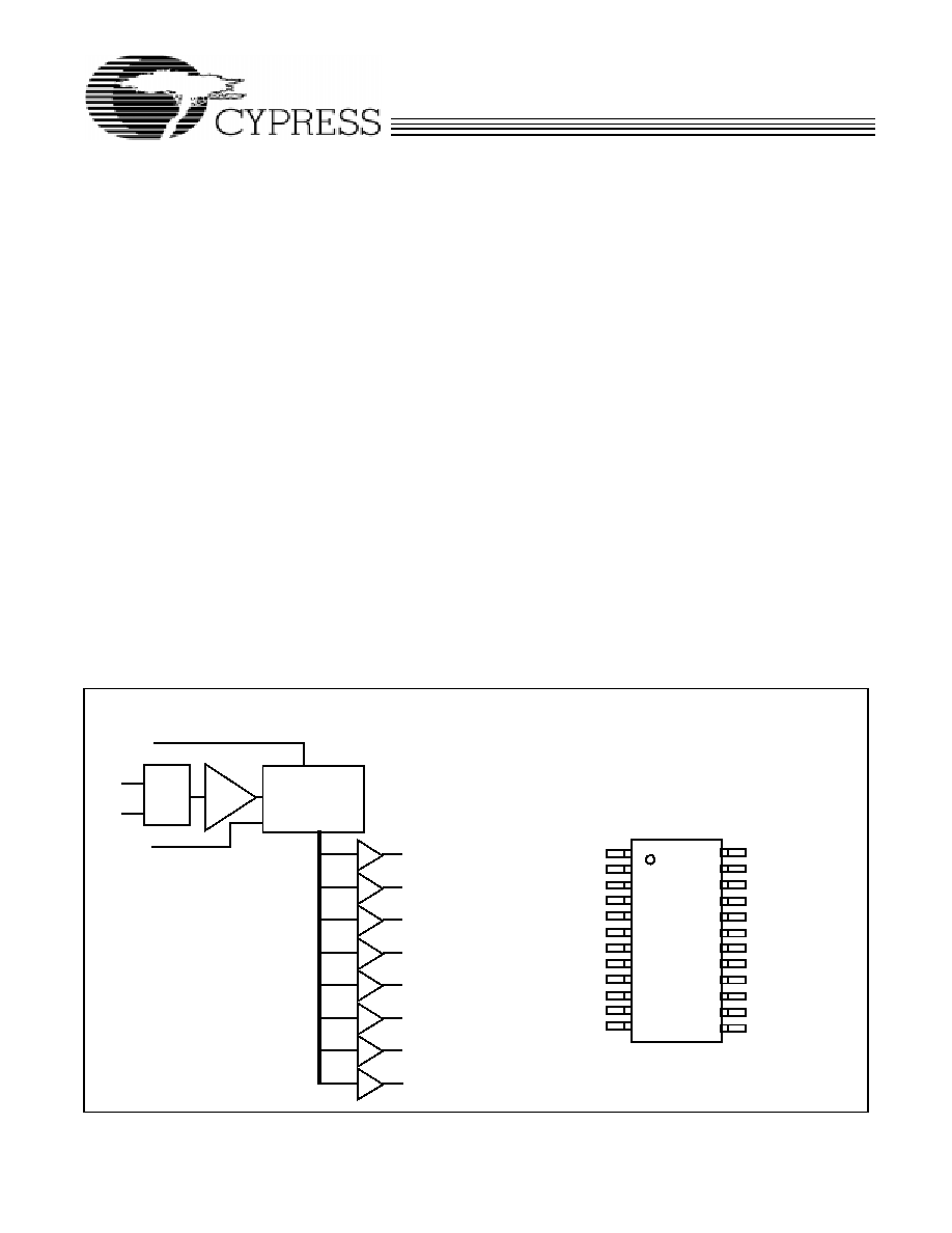
Block Diagram Description
Phase Frequency Detector and Filter
These two blocks accept inputs from the reference frequency
(REF) input and the feedback (FB) input and generate correc-
tion information to control the frequency of the Voltage-Con-
trolled Oscillator (VCO). These blocks, along with the VCO,
form a Phase-Locked Loop (PLL) that tracks the incoming
REF signal.
VCO
The VCO accepts analog control inputs from the PLL filter
block and generates a frequency. The operational range of the
VCO is determined by the FS control pin.
Test Mode
The TEST input is a three-level input. In normal system oper-
ation, this pin is connected to ground, allowing the
CY7B9910/CY7B9920 to operate as explained above. (For
testing purposes, any of the three-level inputs can have a re-
movable jumper to ground, or be tied LOW through a 100
resistor. This will allow an external tester to change the state of
these pins.)
If the TEST input is forced to its MID or HIGH state, the device
will operate with its internal phase-locked loop disconnected,
and input levels supplied to REF will directly control all outputs.
Relative output to output functions are the same as in normal
mode.
Pentium is a trademark of Intel Corporation.
Logic Block Diagram
Pin Configuration
7B99101
7B99102
TEST
FB
REF
Voltage
Controlled
Oscillator
FS
Q0
FILTER
PHASE
FREQ
DET
Q4
Q2
REF
V
CCQ
FS
NC
V
CCQ
V
CCN
Q0
Q1
GND
Q3
V
CCN
GND
TEST
NC
GND
V
CCN
Q7
Q6
GND
Q5
V
CCN
FB
SOIC
Top View
1
2
3
4
5
6
7
8
9
10
11
12
15
16
17
18
19
20
24
23
22
21
13
14
7B9910
7B9920
Q1
Q2
Q3
Q4
Q5
Q6
Q7
CY7B9910
CY7B9920
2
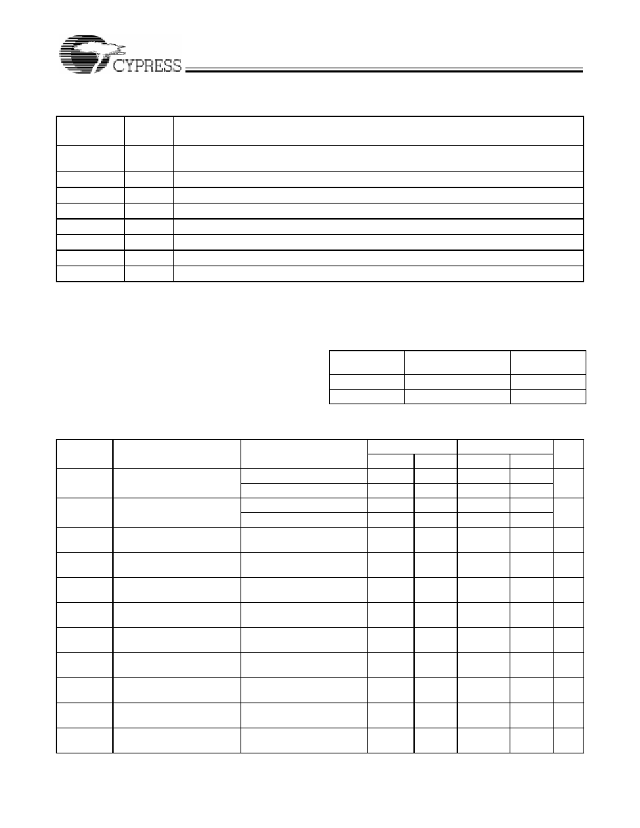
Maximum Ratings
(Above which the useful life may be impaired. For user guide-
lines, not tested.)
Storage Temperature .................................65
°
C to +150
°
C
Ambient Temperature with
Power Applied.............................................55
°
C to +125
°
C
Supply Voltage to Ground Potential............... 0.5V to +7.0V
DC Input Voltage ........................................... 0.5V to +7.0V
Output Current into Outputs (LOW) ............................. 64 mA
Static Discharge Voltage ........................................... >2001V
(per MIL-STD-883, Method 3015)
Latch-Up Current ..................................................... >200 mA
Pin Definitions
Signal
Name
I/O
Description
REF
I
Reference frequency input. This input supplies the frequency and timing against which all functional
variation is measured.
FB
I
PLL feedback input (typically connected to one of the eight outputs).
FS
[9,10,11]
I
Three-level frequency range select.
TEST
I
Three-level select. See Test Mode section.
Q[0..7]
O
Clock outputs.
V
CCN
PWR
Power supply for output drivers.
V
CCQ
PWR
Power supply for internal circuitry.
GND
PWR
Ground.
Operating Range
Range
Ambient
Temperature
V
CC
Commercial
0
°
C to +70
°
C
5V
±
10%
Industrial
40
°
C to +85
°
C
5V
±
10%
Electrical Characteristics
Over the Operating Range
CY7B9910
CY7B9920
Parameter
Description
Test Conditions
Min.
Max.
Min.
Max.
Unit
V
OH
Output HIGH Voltage
V
CC
= Min., I
OH
= 16 mA
2.4
V
V
CC
= Min., I
OH
=40 mA
V
CC
0.75
V
OL
Output LOW Voltage
V
CC
= Min., I
OL
= 46 mA
0.45
V
V
CC
= Min., I
OL
= 46 mA
0.45
V
IH
Input HIGH Voltage
(REF and FB inputs only)
2.0
V
CC
V
CC
1.35
V
CC
V
V
IL
Input LOW Voltage
(REF and FB inputs only)
0.5
0.8
0.5
1.35
V
V
IHH
Three-Level Input HIGH
Voltage (Test, FS)
[1]
Min.
V
CC
Max.
V
CC
1V
V
CC
V
CC
1V
V
CC
V
V
IMM
Three-Level Input MID
Voltage (Test, FS)
[1]
Min.
V
CC
Max.
V
CC
/2
500 mV
V
CC
/2 +
500 mV
V
CC
/2
500 mV
V
CC
/2 +
500 mV
V
V
ILL
Three-Level Input LOW
Voltage (Test, FS)
[1]
Min.
V
CC
Max.
0.0
1.0
0.0
1.0
V
I
IH
Input HIGH Leakage Current
(REF and FB inputs only)
V
CC
= Max., V
IN
= Max.
10
10
µ
A
I
IL
Input LOW Leakage Current
(REF and FB inputs only)
V
CC
= Max., V
IN
= 0.4V
500
500
µ
A
I
IHH
Input HIGH Current
(Test, FS)
V
IN
= V
CC
200
200
µ
A
I
IMM
Input MID Current
(Test, FS)
V
IN
= V
CC
/2
50
50
50
50
µ
A
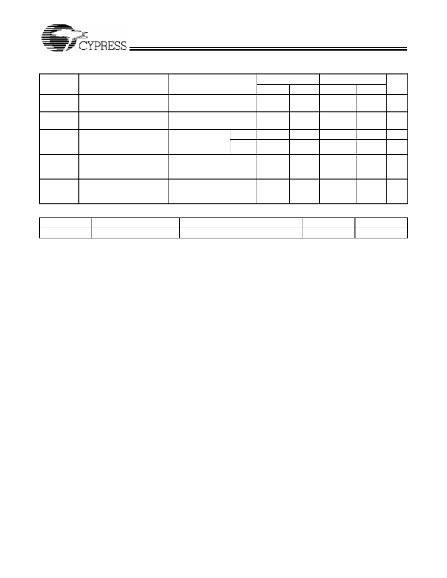
CY7B9910
CY7B9920
3
I
ILL
Input LOW Current
(Test, FS)
V
IN
= GND
200
200
µ
A
I
OS
Output Short Circuit
Current
[2]
V
CC
= Max., V
OUT
= GND (25
°
C only)
250
N/A
mA
I
CCQ
Operating Current Used by
Internal Circuitry
V
CCN
= V
CCQ
= Max.,
All Input
Selects Open
Com'l
85
85
mA
Mil/Ind
90
90
I
CCN
Output Buffer Current per
Output Pair
[3]
V
CCN
= V
CCQ
= Max.,
I
OUT
= 0 mA
Input Selects Open, f
MAX
14
19
mA
PD
Power Dissipation per
Output Pair
[4]
V
CCN
= V
CCQ
= Max.,
I
OUT
= 0 mA
Input Selects Open, f
MAX
78
104
[5]
mW
Electrical Characteristics
Over the Operating Range (continued)
CY7B9910
CY7B9920
Parameter
Description
Test Conditions
Min.
Max.
Min.
Max.
Unit
Capacitance
[6]
Parameter
Description
Test Conditions
Max.
Unit
C
IN
Input Capacitance
T
A
= 25
°
C, f = 1 MHz, V
CC
= 5.0V
10
pF
Notes:
1.
These inputs are normally wired to V
CC
, GND, or left unconnected (actual threshold voltages vary as a percentage of V
CC
). Internal termination resistors hold unconnected
inputs at V
CC
/2. If these inputs are switched, the function and timing of the outputs may glitch and the PLL may require an additional t
LOCK
time before all data sheet limits are
achieved.
2.
Tested one output at a time, output shorted for less than one second, less than 10% duty cycle. Room temperature only. CY7B9920 outputs are not short
circuit protected.
3.
Total output current per output pair can be approximated by the following expression that includes device current plus load current:
CY7B9910:
I
CCN
= [(4 + 0.11F) + [((835 3F)/Z) + (.0022FC)]N] x 1.1
CY7B9920:
I
CCN
= [(3.5+ .17F) + [((1160 2.8F)/Z) + (.0025FC)]N] x 1.1
Where
F = frequency in MHz
C = capacitive load in pF
Z = line impedance in ohms
N = number of loaded outputs; 0, 1, or 2
FC = F
<
C
4.
Total power dissipation per output pair can be approximated by the following expression that includes device power dissipation plus power dissipation due to
the load circuit:
CY7B9910:
PD = [(22 + 0.61F) + [((1550 2.7F)/Z) + (.0125FC)]N] x 1.1
CY7B9920:
PD = [(19.25+ 0.94F) + [((700 + 6F)/Z) + (.017FC)]N] x 1.1
See note 3 for variable definition.
5.
CMOS output buffer current and power dissipation specified at 50-MHz reference frequency.
6.
Applies to REF and FB inputs only. Tested initially and after any design or process changes that may affect these parameters.
CY7B9910
CY7B9920
4
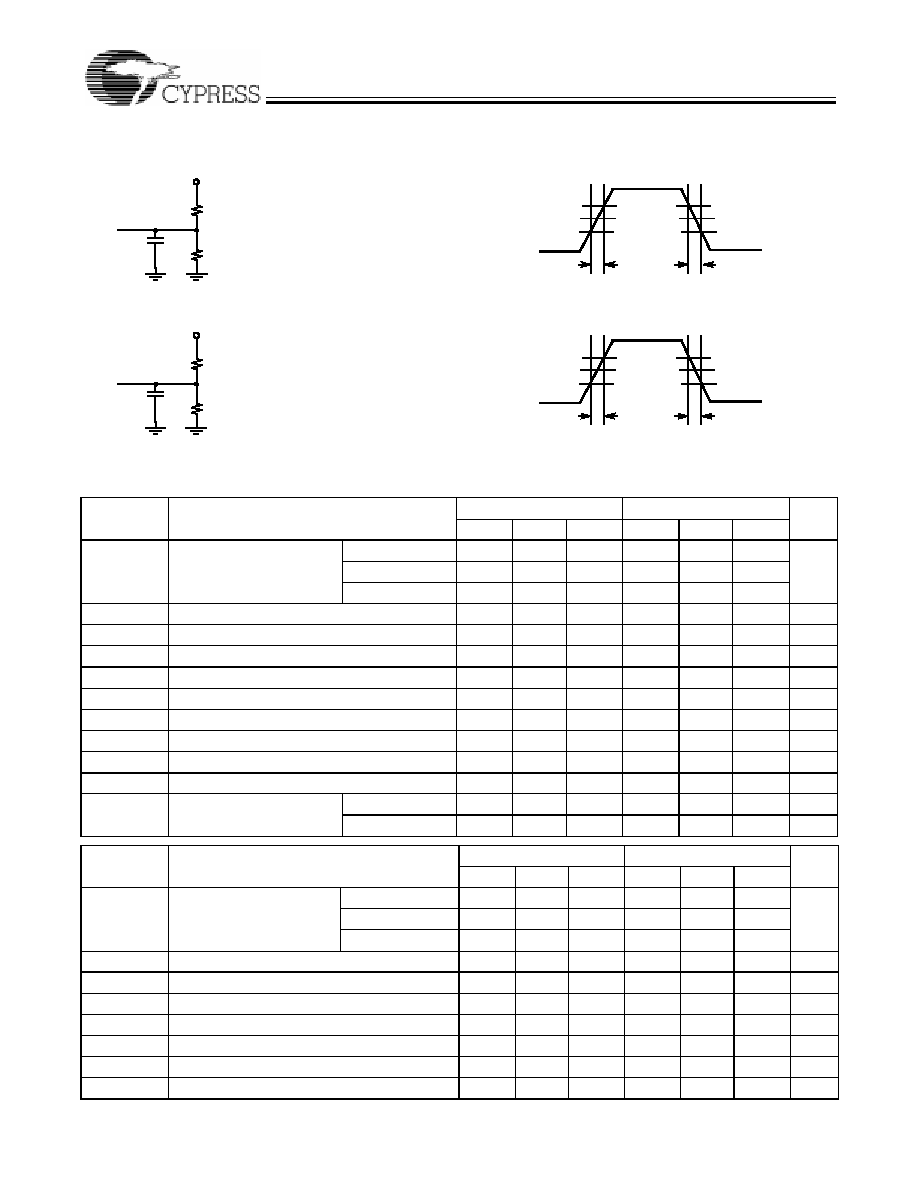
AC Test Loads and Waveforms
7B99103
7B99104
TTL AC Test Load (CY7B9910)
TTL Input Test Waveform (Cy7B9910)
5V
R1
R2
C
L
R1
R2
C
L
7B99105
CMOS AC Test Load (CY7B9920)
3.0V
2.0V
V
th
=1.5V
0.8V
0.0V
1ns
1ns
2.0V
0.8V
V
th
=1.5V
80%
V
th
= V
CC
/2
20%
0.0V
3ns
3ns
80%
20%
V
th
= V
CC
/2
7B99106
CMOS Input Test Waveform (CY7B9920)
V
CC
R1=130
R2=91
C
L
= 50 pF (C
L
= 30pF for 5 and 2 devices)
(Includes fixture and probe capacitance)
R1=100
R2=100
C
L
= 50 pF (C
L
=30 pF for 5 and 2devices)
(Includes fixture and probe capacitance)
V
CC
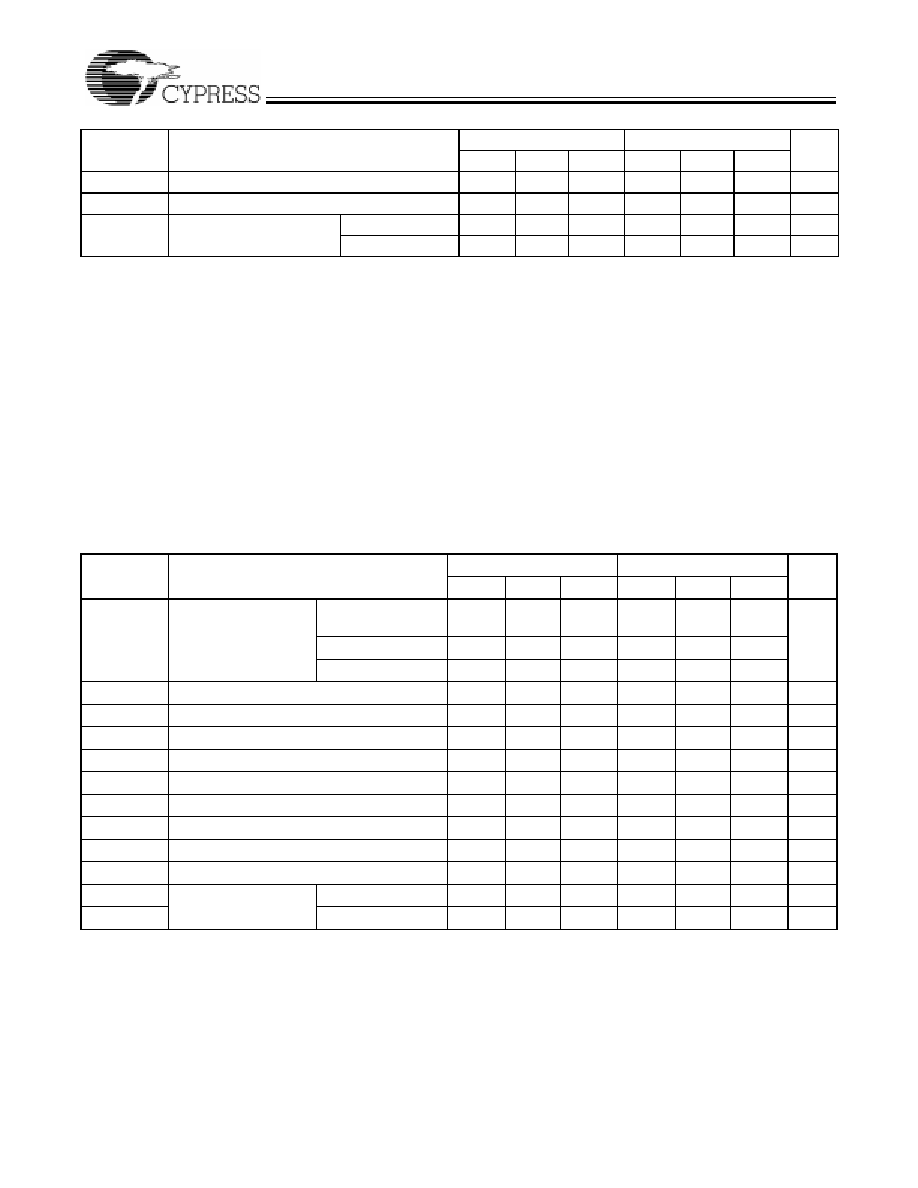
Switching Characteristics
Over the Operating Range
[7]
CY7B99102
[8]
CY7B99202
[8]
Parameter
Description
Min.
Typ.
Max.
Min.
Typ.
Max.
Unit
f
NOM
Operating Clock
Frequency in MHz
FS = LOW
[9, 10]
15
30
15
30
MHz
FS = MID
[9, 10]
25
50
25
50
FS = HIGH
[9, 10, 11]
40
80
40
80
[12]
t
RPWH
REF Pulse Width HIGH
5.0
5.0
ns
t
RPWL
REF Pulse Width LOW
5.0
5.0
ns
t
SKEW
Zero Output Skew (All Outputs)
[13, 14]
0.1
0.25
0.1
0.25
ns
t
DEV
Device-to-Device Skew
[14, 15]
0.75
0.75
ns
t
PD
Propagation Delay, REF Rise to FB Rise
0.25
0.0
+0.25
0.25
0.0
+0.25
ns
t
ODCV
Output Duty Cycle Variation
[16]
0.65
0.0
+0.65
0.65
0.0
+0.65
ns
t
ORISE
Output Rise Time
[17, 18]
0.15
1.0
1.2
0.5
2.0
2.5
ns
t
OFALL
Output Fall Time
[17, 18]
0.15
1.0
1.2
0.5
2.0
2.5
ns
t
LOCK
PLL Lock Time
[19]
0.5
0.5
ms
t
JR
Cycle-to-Cycle Output Jitter Peak to Peak
200
200
ps
RMS
25
25
ps
CY7B99105
CY7B99205
Parameter
Description
Min.
Typ.
Max.
Min.
Typ.
Max.
Unit
f
NOM
Operating Clock
Frequency in MHz
FS = LOW
[9, 10]
15
30
15
30
MHz
FS = MID
[9, 10]
25
50
25
50
FS = HIGH
[9, 10, 11]
40
80
40
80
[12]
t
RPWH
REF Pulse Width HIGH
5.0
5.0
ns
t
RPWL
REF Pulse Width LOW
5.0
5.0
ns
t
SKEW
Zero Output Skew (All Outputs)
[13, 14]
0.25
0.5
0.25
0.5
ns
t
DEV
Device-to-Device Skew
[8, 15]
1.0
1.0
ns
t
PD
Propagation Delay, REF Rise to FB Rise
0.5
0.0
+0.5
0.5
0.0
+0.5
ns
t
ODCV
Output Duty Cycle Variation
[16]
1.0
0.0
+1.0
1.0
0.0
+1.0
ns
t
ORISE
Output Rise Time
[17, 18]
0.15
1.0
1.5
0.5
2.0
3.0
ns
CY7B9910
CY7B9920
5
t
OFALL
Output Fall Time
[17, 18]
0.15
1.0
1.5
0.5
2.0
3.0
ns
t
LOCK
PLL Lock Time
[19]
0.5
0.5
ms
t
JR
Cycle-to-Cycle Output Jitter Peak to Peak
[8]
200
200
ps
RMS
[8]
25
25
ps
Notes:
7.
Test measurement levels for the CY7B9910 are TTL levels (1.5V to 1.5V). Test measurement levels for the CY7B9920 are CMOS levels (V
CC
/2 to V
CC
/2). Test
conditions assume signal transition times of 2ns or less and output loading as shown in the AC Test Loads and Waveforms unless otherwise specified.
8.
Guaranteed by statistical correlation. Tested initially and after any design or process changes that may affect these parameters.
9.
For all three-state inputs, HIGH indicates a connection to V
CC
, LOW indicates a connection to GND, and MID indicates an open connection. Internal termination circuitry
holds an unconnected input to V
CC
/2.
10. The level to be set on FS is determined by the "normal" operating frequency (f
NOM
) of the VCO
(see Logic Block Diagram). The frequency appearing at the REF and
FB inputs will be f
NOM
when the output connected to FB is undivided. The frequency of the REF and FB inputs will be f
NOM
/X
when the device is configured for a frequency
multiplication by using external division in the feedback path of value X.
11. When the FS pin is selected HIGH, the REF input must not transition upon power-up until V
CC
has reached 4.3V.
12. Except as noted, all CY7B99202 and 5 timing parameters are specified to 80-MHz with a 30-pF load.
13. t
SKEW
is defined as the time between the earliest and the latest output transition among all outputs when all are loaded with 50 pF and terminated with 50
to
2.06V (CY7B9910) or V
CC
/2 (CY7B9920).
14. t
SKEW
is defined as the skew between outputs.
15. t
DEV
is the output-to-output skew between any two outputs on separate devices operating under the same conditions (V
CC
, ambient temperature, air flow, etc.).
16. t
ODCV
is the deviation of the output from a 50% duty cycle.
17. Specified with outputs loaded with 30 pF for the CY7B99X02 and 5 devices and 50 pF for the CY7B99X07 devices. Devices are terminated through 50
to 2.06V (CY7B9910) or V
CC
/2 (CY7B9920).
18. t
ORISE
and t
OFALL
measured between 0.8V and 2.0V for the CY7B9910 or 0.8V
CC
and 0.2V
CC
for the CY7B9920.
19. t
LOCK
is the time that is required before synchronization is achieved. This specification is valid only after V
CC
is stable and within normal operating limits. This parameter is
measured from the application of a new signal or frequency at REF or FB until t
PD
is within specified limits.
CY7B99105
CY7B99205
Parameter
Description
Min.
Typ.
Max.
Min.
Typ.
Max.
Unit
Switching Characteristics
Over the Operating Range
[7]
(continued)
CY7B99107
CY7B99207
Parameter
Description
Min.
Typ.
Max.
Min.
Typ.
Max.
Unit
f
NOM
Operating Clock
Frequency in MHz
FS = LOW
[9, 10]
15
30
15
30
MHz
FS = MID
[9, 10]
25
50
25
50
FS = HIGH
[9, 10, 11]
40
80
40
80
[12]
t
RPWH
REF Pulse Width HIGH
5.0
5.0
ns
t
RPWL
REF Pulse Width LOW
5.0
5.0
ns
t
SKEW
Zero Output Skew (All Outputs)
[13, 14]
0.3
0.75
0.3
0.75
ns
t
DEV
Device-to-Device Skew
[8, 15]
1.5
1.5
ns
t
PD
Propagation Delay, REF Rise to FB Rise
0.7
0.0
+0.7
0.7
0.0
+0.7
ns
t
ODCV
Output Duty Cycle Variation
[16]
1.2
0.0
+1.2
1.2
0.0
+1.2
ns
t
ORISE
Output Rise Time
[17, 18]
0.15
1.5
2.5
0.5
3.0
5.0
ns
t
OFALL
Output Fall Time
[17, 18]
0.15
1.5
2.5
0.5
3.0
5.0
ns
t
LOCK
PLL Lock Time
[19]
0.5
0.5
ms
t
JR
Cycle-to-Cycle Output
Jitter
Peak to Peak
[8]
200
200
ps
t
JR
RMS
[8]
25
25
ps
CY7B9910
CY7B9920
6
AC Timing Diagrams
t
ODCV
t
ODCV
t
REF
REF
FB
Q
OTHER Q
t
RPWH
t
RPWL
t
PD
t
SKEW
t
SKEW
t
JR
7B99108
CY7B9910
CY7B9920
© Cypress Semiconductor Corporation, 1997. The information contained herein is subject to change without notice. Cypress Semiconductor Corporation assumes no responsibility for the use
of any circuitry other than circuitry embodied in a Cypress Semiconductor product. Nor does it convey or imply any license under patent or other rights. Cypress Semiconductor does not authorize
its products for use as critical components in life-support systems where a malfunction or failure may reasonably be expected to result in significant injury to the user. The inclusion of Cypress
Semiconductor products in life-support systems application implies that the manufacturer assumes all risk of such use and in doing so indemnifies Cypress Semiconductor against all charges.
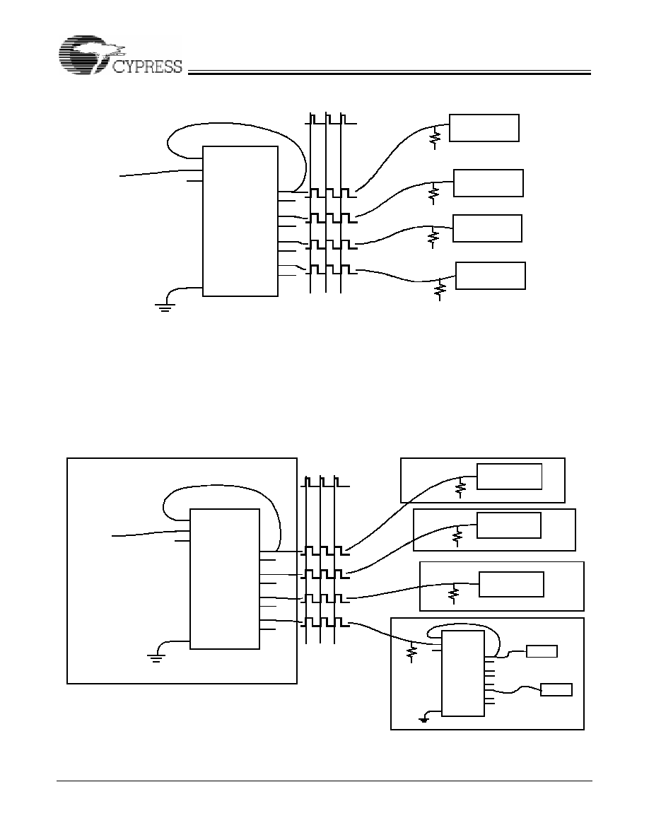
Operational Mode Descriptions
Figure 1 shows the device configured as a zero-skew clock
buffer. In this mode the 7B9910/9920 can be used as the basis
for a low-skew clock distribution tree. The outputs are aligned
and may each drive a terminated transmission line to an inde-
pendent load. The FB input can be tied to any output and the
operating frequency range is selected with the FS pin. The
low-skew specification, coupled with the ability to drive termi-
nated transmission lines (with impedances as low as 50
ohms), allows efficient printed circuit board design.
Figure 2 shows the CY7B9910/9920 connected in series to
construct a zero-skew clock distribution tree between boards.
Cascaded clock buffers will accumulate low-frequency jitter
because of the non-ideal filtering characteristics of the PLL
filter. It is not recommended that more than two clock buffers
be connected in series.
Figure 1. Zero-Skew and/or Zero-Delay Clock Driver
SYSTEM
CLOCK
7B99109
FB
REF
FS
Q0
Q1
Q2
Q3
Q4
Q5
Q6
Q7
TEST
Z
0
LOAD
LOAD
LOAD
LOAD
REF
Z
0
Z
0
Z
0
Figure 2. Board-to-Board Clock Distribution
SYSTEM
CLOCK
Z
0
7B991010
FB
REF
FS
TEST
REF
REF
FS
FB
LOAD
LOAD
LOAD
LOAD
LOAD
TEST
Z
0
Z
0
Z
0
Q0
Q1
Q2
Q3
Q4
Q5
Q6
Q7
Q0
Q1
Q2
Q3
Q4
Q5
Q6
Q7
CY7B9910
CY7B9920
8
Document #: 3800437B
Ordering Information
Accuracy
(ps)
Ordering Code
Package
Name
Package Type
Operating
Range
250
CY7B99102SC
S13
24-Lead Small Outline IC
Commercial
CY7B99202SC
S13
24-Lead Small Outline IC
500
CY7B99105SC
S13
24-Lead Small Outline IC
Commercial
CY7B99105SI
S13
24-Lead Small Outline IC
Industrial
CY7B99205SC
S13
24-Lead Small Outline IC
Commercial
CY7B99205SI
S13
24-Lead Small Outline IC
Industrial
750
CY7B99107SC
S13
24-Lead Small Outline IC
Commercial
CY7B99107SI
S13
24-Lead Small Outline IC
Industrial
CY7B99207SC
S13
24-Lead Small Outline IC
Commercial
CY7B99207SI
S13
24-Lead Small Outline IC
Industrial
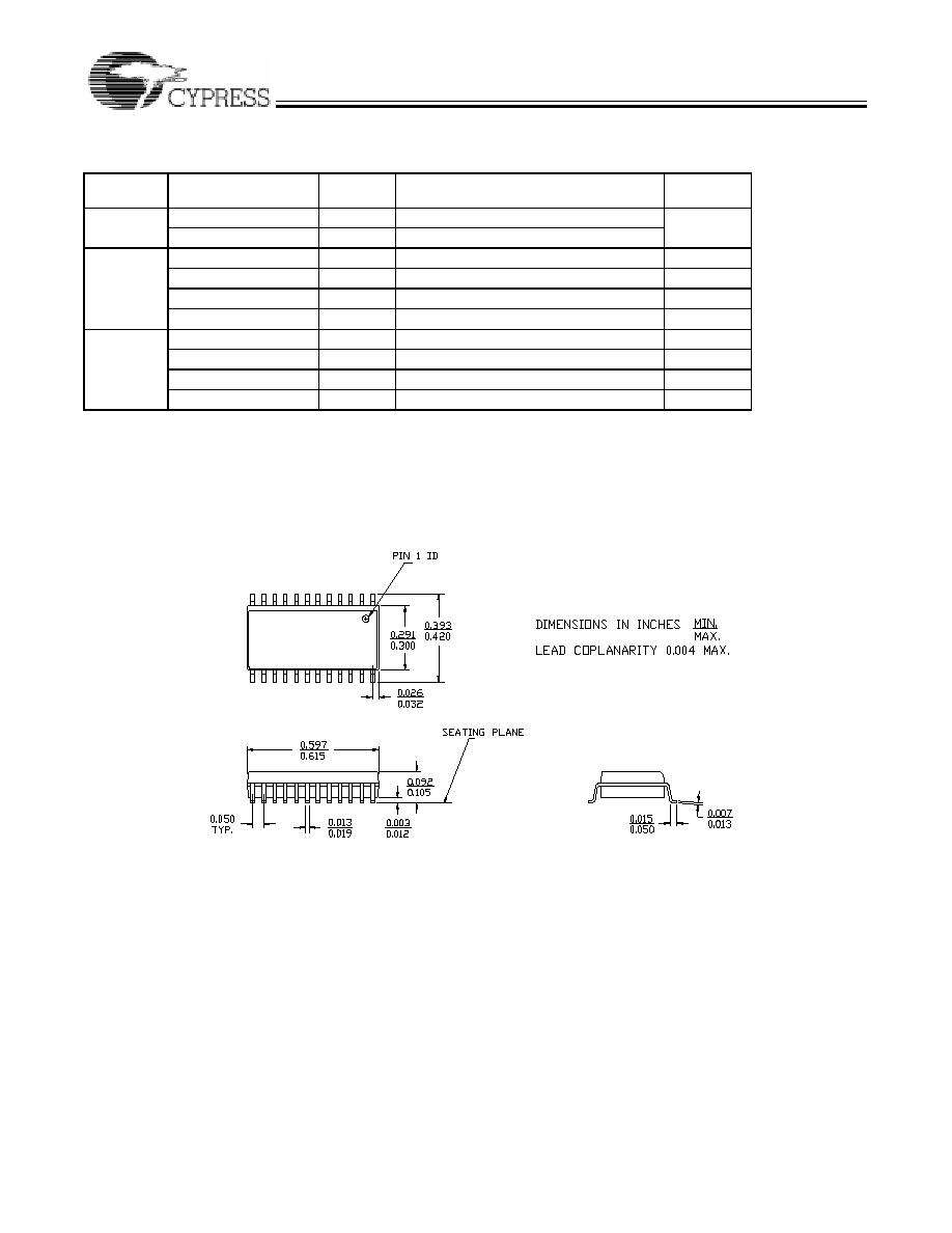
Package Diagram
24-Lead (300-Mil) Molded SOIC S13