 | ÐлекÑÑоннÑй компоненÑ: CY7B995AC | СкаÑаÑÑ:  PDF PDF  ZIP ZIP |
Äîêóìåíòàöèÿ è îïèñàíèÿ www.docs.chipfind.ru
2.5/3.3V 200-MHz High-Speed Multi-Phase
PLL Clock Buffer
CY7B995
Cypress Semiconductor Corporation
·
3901 North First Street
·
San Jose
,
CA 95134
·
408-943-2600
Document #: 38-07337 Rev. *A
Revised February 24, 2004
Features
· 2.5V or 3.3V operation
· Split output bank power supplies
· Output frequency range: 6 MHz to 200 MHz
· Output-output skew < 100 ps
· Cycle-cycle jitter <100 ps
· ± 2% max output duty cycle
· Selectable output drive strength
· Selectable positive or negative edge synchronization
· Eight LVTTL outputs driving 50
terminated lines
· LVCMOS/LVTTL over-voltage tolerant reference input
· Selectable phase-locked loop (PLL) frequency range
and lock indicator
· Phase adjustments in 625/1250 ps steps up to ± 7.5 ns
· (1-6,8,10,12) x multiply and (1/2,1/4)x divide ratios
· Spread-Spectrum-compatible
· Power-down mode
· Selectable reference divider
· Industrial temperature range: -40°C to +85°C
· 44-pin TQFP package
Description
The CY7B995 RoboClock is a low-voltage, low-power,
eight-output, 200-MHz clock driver. It features output phase
programmability which is necessary to optimize the timing of
high-performance computer and communication systems.
The user can program both the frequency and the phase of the
output banks through nF[0:1] and DS[0:1] pins. The adjustable
phase feature allows the user to skew the outputs to lead or
lag the reference clock. Any one of the outputs can be con-
nected to feedback input to achieve different reference fre-
quency multiplication and divide ratios and zero input-output
delay.
The device also features split output bank power supplies
which enable the user to run two banks (1Qn and 2Qn) at a
power supply level different from that of the other two banks
(3Qn and 4Qn). Additionally, the three-level PE/HD pin con-
trols the synchronization of the output signals to either the ris-
ing or the falling edge of the reference clock and selects the
drive strength of the output buffers. The high drive option
(PE/HD = MID) increases the output current from ± 12 mA to
± 24 mA
(3.3V).
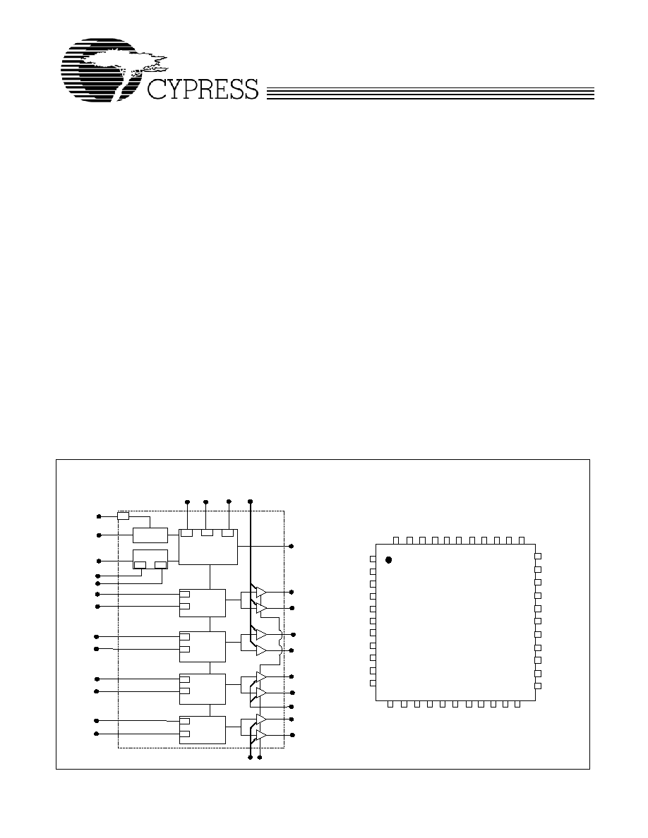
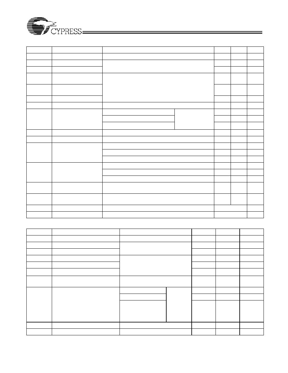
Block Diagram
Pin Configuration
PE/HD
TEST
FS
3
3
REF
FB
2F1:0
1F1:0
3F1:0
4F1:0
1Q0
1Q1
2Q0
2Q1
3Q0
3Q1
4Q0
4Q1
PLL
3
3
3
3
3
3
3
3
Phase
Select
Phase
Select
Phase
Select
and /K
3
sOE#
VDDQ1
VDDQ4
LOCK
/N
3
3
/R
3
PD#/DIV
DS1:0
Phase
Select
and /M
VDDQ3
CY7B995
33
32
31
30
29
28
27
26
25
24
23
1F0
DS1
DS0
LOCK
VDDQ1
VDDQ1
1Q0
1Q1
VSS
VSS
VSS
44 43 42 41 40 39 38 37 36 35 34
3F
1
VDD
VSS TES T
4F
0
3F
0
FS
REF
2F
1
2F
0
1F
1
1
2
3
4
5
6
7
8
9
10
11
4F1
sOE#
PD#/DIV
PE/HD
VDDQ4
4Q1
4Q0
VSS
VSS
VSS
VDDQ4
12 13 14 15 16 17 18 19 20 21 22
VSS
3Q
1
3Q
0
VD
DQ
3
VD
DQ
3
FB
VD
D
VD
DQ
1
2Q
1
2Q
0
VSS
CY7B995
Document #: 38-07337 Rev. *A
Page 2 of 11
Device Configuration
The outputs of the CY7B995 can be configured to run at
frequencies ranging from 6 MHz to 200 MHz. The feedback
input divider is controlled by the 3-level DS[0:1] pins as
indicated in Table 2 and the reference input divider is
controlled by the 3-level PD#/DIV pin as indicated in Table 1.
Notes:
1. `PD' indicates an internal pull-down and `PU' indicates an internal pull-up.
2. A bypass capacitor (0.1
µF) should be placed as close as possible to each positive power pin (< 0.2"). If these bypass capacitors are not close to the pins their
high frequency filtering characteristic will be cancelled by the lead inductance of the traces.
3. When TEST = MID and sOE# = HIGH, PLL remains active with nF[1:0] = LL functioning as an output disable control for individual output banks. Skew selections
remain in effect unless nF[1:0] = LL.
Pin Description
Pin
Name
I/O
[1]
Type
Description
39
REF
I
LVTTL/LVCMOS
Reference Clock Input.
17
FB
I
LVTTL
Feedback Input.
37
TEST
I
3-Level
When MID or HIGH, disables PLL (except for conditions of note 3).
REF goes to all outputs. Set LOW for normal operation.
2
sOE#
I, PD LVTTL
Synchronous Output Enable. When HIGH, it stops clock outputs
(except 2Q0 and 2Q1) in a LOW state (for PE/HD = H or M) 2Q0 and
2Q1 may be used as the feedback signal to maintain phase lock. When
TEST is held at MID level and sOE# is high, the nF[1:0] pins act as output
disable controls for individual banks when nF[1:0] = LL. Set sOE# LOW
for normal operation.
4
PE/HD
I, PU 3-Level
Selects Positive or Negative Edge Control and High or Low output
drive strength. When LOW / HIGH the outputs are synchronized with the
negative / positive edge of the reference clock, respectively. When at MID
level, the output drive strength is increased and the outputs synchronize
with the positive edge of the reference clock. Please see Table 9.
34, 33, 36, 35,
43, 42, 1, 44
nF[1:0]
I
3-Level
Select frequency and phase of the outputs. Please see Tables 3, 4, 5,
7, and 8.
41
FS
I
3-Level
Selects VCO operating frequency range. Please see Table 6.
26,27,20,21,
13,14,7,8
nQ[1:0]
O
LVTTL
Four banks of two outputs. Please see Table 5 for frequency settings.
32, 31
DS[1:0]
I
3-Level
Select feedback divider. Please see Table 2.
3
PD#/DIV
I, PU 3-Level
Power down and reference divider control. When LOW, shuts off entire
chip. When at MID level, enables the reference divider. Please see Table 1
for settings.
30
LOCK
O
LVTTL
PLL lock indication signal. HIGH indicates lock. LOW indicates that the
PLL is not locked and outputs may not be synchronized to the input.
5,6
V
DD
Q4
[2]
PWR Power
Power supply for Bank 4 output buffers. Please see Table 10 for supply
level constraints
15,16
V
DD
Q3
[2]
PWR Power
Power supply for Bank 3 output buffers. Please see Table 10 for supply
level constraints
19,28,29
V
DD
Q1
[2]
PWR Power
Power supply for Bank 1 and Bank 2 output buffers. Please see
Table 10 for supply level constraints
18,40
V
DD
[2]
PWR Power
Power supply for the internal circuitry. Please see Table 10 for supply
level constraints
9-12, 22-25, 38 V
SS
PWR Power
Ground.
Table 1. Reference Divider Settings
PD#/DIV
RReference Divider
H
1
M
2
L
[4]
N/A
CY7B995
Document #: 38-07337 Rev. *A
Page 3 of 11
In addition to the reference and feedback dividers, the
CY7B995 includes output dividers on Bank3 and Bank4, which
are controlled by 3F[1:0] and 4F[1:0] as indicated in Table 3
and 4, respectively.
The divider settings and the FB input to ANY output
connection needed to produce various output frequencies are
summarized in Table 5.
The 3-level FS control pin setting determines the nominal
operating frequency range of the divide-by-one outputs of the
device. The CY7B995 PLL operating frequency range that
corresponds to each FS level is given in Table 6.
Selectable output skew is in discrete increments of time unit
(t
U
).The value of t
U
is determined by the FS setting and the
maximum nominal frequency. The equation to be used to
determine the t
U
value is as follows:
t
U
= 1 / (f
NOM
x MF)
where MF is a multiplication factor, which is determined by the
FS setting as indicated in Table 7.I
Notes:
4. When PD#/DIV = LOW, the device enters power-down mode
5. These states are used to program the phase of the respective banks. Please see Table 7 and Table 8.
6. These outputs are undivided copies of the VCO clock. Therefore, the formulas in this column can be used to calculate the VCO operating frequency (FNOM) at
a given reference frequency (FREF) and divider and feedback configuration. The user must select a configuration and a reference frequency that will generate a
VCO frequency that is within the range specified by FS pin. Please see Table 6.
Table 2. Feedback Divider Settings
DS[1:0]
N-Feedback Input
Divider
Permitted Output Di-
vider Connected to FB
LL
2
1 or 2
LM
3
1
LH
4
1,2 or 4
ML
5
1 or 2
MM
1
1,2 or 4
MH
6
1 or 2
HL
8
1 or 2
HM
10
1
HH
12
1
Table 3. Output Divider Settings Bank 3
3F[1:0]
K - Bank3 Output Divider
LL
2
HH
4
Other
[5]
1
Table 4. Output Divider Settings Bank 4
4F[1:0]
M- Bank4 Output Divider
LL
2
Other
[5]
1
Table 5. Output Frequency Settings
Configuration
Output Frequency
FB Input Con-
nected to
1Q[0:1] and
2Q[0:1]
[6]
3Q[0:1]
4Q[0:1]
1Qn or 2Qn
(N / R) x F
REF
(N / R) x (1 /
K) x F
REF
(N / R) x (1 /
M) x F
REF
3Qn
(N / R) x K x
F
REF
(N / R) x F
REF
(N / R) x (K /
M) x F
REF
4Qn
(N / R) x M x
F
REF
(N / R) x (M /
K) x F
REF
(N / R) x F
REF
Table 6. Frequency Range Select
FS
PLL Frequency Range
L
24 to 50MHz
M
48 to 100MHz
H
96 to 200MHz
Table 7. MF Calculation
FS
MF
f
NOM
at which t
U
is 1.0ns(MHz)
L
32
31.25
M
16
62.5
H
8
125
CY7B995
Document #: 38-07337 Rev. *A
Page 4 of 11
In addition to determining whether the outputs synchronize to
the rising or the falling edge of the reference signal, the 3-level
PE/HD pin controls the output buffer drive strength as
indicated in Table 9.
The CY7B995 features split power supply buses for Banks 1
and 2, Bank 3 and Bank 4, which enables the user to obtain
both 3.3V and 2.5V output signals from one device. The core
power supply (V
DD
) must be set a level which is equal or higher
than that on any one of the output power supplies.
Governing Agencies
The following agencies provide specifications that apply to the
CY7B995. The agency name and relevant specification is
listed below.
Table 8. Output Skew Settings
nF[1:0]
Skew
(1Q[0:1],2Q[0:1])
Skew
(3Q[0:1])
Skew
(4Q[0:1])
LL
[7]
4t
U
Divide By 2
Divide By 2
LM
3t
U
6t
U
6t
U
LH
2t
U
4t
U
4t
U
ML
1t
U
2t
U
2t
U
MM
Zero Skew
Zero Skew
Zero Skew
MH
+1t
U
+2t
U
+2t
U
HL
+2t
U
+4t
U
+4t
U
HM
+3t
U
+6t
U
+6t
U
HH
+4t
U
Divide By 4
Inverted
[8]
Table 9. PE/HD Settings
PE/HD
Synchronization
Output Drive Strength
[9]
L
Negative
Low Drive
M
Positive
High Drive
H
Positive
Low Drive
Table 10.Power Supply Constraints
V
DD
V
DD
Q1
[10]
V
DD
Q3
[10]
V
DD
Q4
[10]
3.3V
3.3V or 2.5V
3.3V or 2.5V
3.3V or 2.5V
2.5V
2.5V
2.5V
2.5V
Table 11.
Agency Name
Specification
JEDEC
JESD 51 (Theta JA)
JESD 65 (Skew, Jitter)
IEEE
1596.3 (Jiter Specs)
UL-194_V0
94 (Moisture Grading)
MIL
883E Method 1012.1
(Therma Theta JC)
Absolute Maximum Conditions
Parameter
Description
Condition
Min.
Max.
Unit
V
DD
Operating Voltage
Functional @ 2.5V ± 5%
2.25
2.75
V
V
DD
Operating Voltage
Functional @ 3.3V ± 10%
2.97
3.63
V
V
IN(MIN)
Input Voltage
Relative to V
SS
V
SS
0.3
V
V
IN(MAX)
Input Voltage
Relative to V
DD
V
DD
+0.3
V
V
REF(MAX)
Reference Input Voltage
V
DD
= 3.3V
5.5
V
V
REF(MAX)
Reference Input Voltage
V
DD
= 2.5V
4.6
V
T
S
Temperature, Storage
Non Functional
65
+150
°C
T
A
Temperature, Operating Ambient
Functional
40
+85
°C
T
J
Temperature, Junction
Functional
155
°C
Ø
JC
Dissipation, Junction to Case
Mil-Spec 883E Method 1012.1
42
°C/W
Ø
JA
Dissipation, Junction to Ambient
JEDEC (JESD 51)
74
°C/W
ESD
HBM
ESD Protection (Human Body Model)
MIL-STD-883, Method 3015
2000
V
UL-94
Flammability Rating
@1/8 in.
V0
MSL
Moisture Sensitivity Level
1
F
IT
Failure in Time
Manufacturing Testing
10
ppm
Notes:
7. LL disables outputs if TEST = MID and sOE# = HIGH.
8. When 4Q[0:1] are set to run inverted (HH mode), sOE# disables these outputs HIGH when PE/HD = HIGH or MID, sOE# disables them LOW when PE/HD = LOW.
9. Please refer to "DC Parameters" section for IOH/IOL specifications.
10.
V
DDQ1/3/4 must not be set at a level higher than that of
V
DD. They can be set at different levels from each other, e.g.,
V
DD = 3.3V,
V
DDQ1 = 3.3V,
V
DDQ3
= 2.5V and
V
DDQ4 = 2.5V.
CY7B995
Document #: 38-07337 Rev. *A
Page 5 of 11
.
DC Specifications @ 2.5V
Parameter
Description
Conditions
Min.
Max.
Unit
V
DD
2.5 Operating Voltage
2.5V ± 5%
2.375
2.625
V
V
IL
Input LOW Voltage
REF, FB and sOE# Inputs
0.7
V
V
IH
Input HIGH Voltage
1.7
V
V
IHH
[11]
Input HIGH Voltage
3-Level Inputs, (TEST, FS, nF[1:0], DS[1:0], PD#/DIV,
PE/HD). (These pins are normally wired to VDD, GND, or
unconnected)
V
DD
0.4
V
V
IMM
[11]
Input MID Voltage
V
DD
/2
0.2
V
DD
/2
+ 0.2
V
V
ILL
[11]
Input LOW Voltage
0.4
V
I
IL
Input Leakage Current
V
IN
= V
DD
/G
ND
,V
DD
= Max; (REF and FB inputs)
5
5
µA
I
3
3-Level Input DC Current
HIGH, V
IN
= V
DD
3-Level Inputs
(TEST, FS, nF[1:0],
DS[1:0], PD#/DIV,
PE/HD)
200
µA
MID, V
IN
= V
DD
/2
50
50
µA
LOW, V
IN
= V
SS
200
µA
I
PU
Input Pull-Up Current
V
IN
= V
SS
, V
DD
= Max
25
µA
I
PD
Input Pull-Down Current
V
IN
= V
DD
, V
DD
= Max, (sOE#)
100
µA
V
OL
Output LOW Voltage
I
OL
= 12mA (PE/HD = L/H), (nQ[0:1])
0.4
V
I
OL
= 20mA (PE/HD = MID),(nQ[0:1])
0.4
V
I
OL
= 2mA (LOCK)
0.4
V
V
OH
Output HIGH Voltage
I
OH
= 12mA (PE/HD = L/H),(nQ[0:1])
2.0
V
I
OH
= 20mA (PE/HD = MID),(nQ[0:1])
2.0
V
I
OH
= 2mA (LOCK)
2.0
V
I
DDQ
Quiescent Supply Current
VDD = Max, TEST = MID, REF = LOW, sOE# = LOW,
Outputs not loaded
2
mA
I
DDPD
Power-down Current
PD#/DIV, sOE# = LOW
Test,nF[1:0],DS[1:0] = HIGH; V
DD
= Max
10(typ.)
25
µA
I
DD
Dynamic Supply Current @100MHz
150
mA
C
IN
Input Pin Capacitance
4
pF
DC Specifications @ 3.3V
Parameter
Description
Condition
Min.
Max.
Unit
V
DD
3.3 Operating Voltage
3.3V ± 10%
2.97
3.63
V
V
IL
Input LOW Voltage
REF, FB and sOE# Inputs
0.8
V
V
IH
Input HIGH Voltage
2.0
V
V
IHH
[11]
Input HIGH Voltage
3-Level Inputs
(TEST, FS, nF[1:0], DS[1:0],PD#/DIV,
PE/HD); (These pins are normally
wired to VDD,GND or unconected
V
DD
0.6
V
V
IMM
[11]
Input MID Voltage
V
DD
/2 0.3 V
DD
/2 + 0.3
V
V
ILL
[11]
Input LOW Voltage
0.6
V
I
IL
Input Leakage Current
V
IN
= V
DD
/G
ND
,V
DD
= Max
(REF and FB inputs)
5
5
µA
I
3
3-Level Input DC Current
HIGH, V
IN
= V
DD
3-Level
Inputs,
(TEST, FS,
nF[1:0],
DS[1:0],
PD#/DIV,
PE/HD)
200
µA
MID, V
IN
= V
DD
/2
50
50
µA
LOW, V
IN
= V
SS
200
µA
I
PU
Input Pull-Up Current
V
IN
= V
SS
, V
DD
= Max
25
µA
I
PD
Input Pull-Down Current
V
IN
= V
DD
, V
DD
= Max, (sOE#)
100
µA
Note:
11. These Inputs are normally wired to VDD, GND or unconnected. Internal termination resistors bias unconnected inputs to VDD/2.
CY7B995
Document #: 38-07337 Rev. *A
Page 6 of 11
V
OL
Output LOW Voltage
I
OL
= 12 mA (PE/HD = L/H), (nQ[0:1])
0.4
V
I
OL
= 24 mA (PE/HD = MID),(nQ[0:1])
0.4
V
I
OL
= 2 mA (LOCK)
0.4
V
V
OH
Output HIGH Voltage
I
OH
= 12 mA (PE/HD = L/H),(nQ[0:1])
2.4
V
I
OH
= 24 mA (PE/HD =
MID),(nQ[0:1])
2.4
V
I
OH
= 2 mA (LOCK)
2.4
V
I
DDQ
Quiescent Supply Current
VDD = Max, TEST = MID, REF =
LOW, sOE# = LOW, Outputs not
loaded
2
mA
I
DDPD
Power Down Current
PD#/DIV, sOE# = LOW,
Test,nF[1:0],DS[1:0] = HIGH, V
DD
=
Max
10(typ.)
25
µA
I
DD
Dynamic Supply Current
@100 MHz
230
mA
C
IN
Input Pin Capacitance
4
pF
AC Input Specifications
Parameter
Description
Condition
Min.
Max.
Unit
T
R
,T
F
Input Rise/Fall Time
0.8V 2.0V
10
ns/V
T
PWC
Input Clock Pulse
HIGH or LOW
2
ns
T
DCIN
Input Duty Cycle
10
90
%
F
REF
Reference Input Frequency
[12]
FS = LOW
2
50
MHz
FS = MID
4
100
FS = HIGH
8
200
Switching Characteristics
Parameter
Description
Condition
Min.
Max.
Unit
F
OR
Output frequency range
6
200
MHz
VCO
LR
VCO Lock Range
200
400
MHz
VCO
LBW
VCO Loop Bandwidth
0.25
3.5
MHz
t
SKEWPR
Matched-Pair Skew
[13]
Skew between the earliest and the latest
output transitions within the same bank.
100
ps
t
SKEW0
Output-Output Skew
[13]
Skew between the earliest and the latest
output transitions among all outputs at 0t
U
.
200
ps
t
SKEW1
Skew between the earliest and the latest
output transitions among all outputs for
which the same phase delay has been
selected.
200
ps
t
SKEW2
Skew between the nominal output rising
edge to the inverted output falling edge
500
ps
t
SKEW3
Skew between non-inverted outputs
running at different frequencies
500
ps
t
SKEW4
Output-Output Skew
[13]
Skew between nominal to inverted outputs
running at different frequencies
500
ps
t
SKEW5
Skew between nominal outputs at different
power supply levels
650
ps
Notes:
12. IF PD#/DIV is in HIGH level (R-reference divider = 1). Reference Input Frequency = F
REF.
IF PD#/DIV is in MID level (R-reference divider = 2). Reference Input
Frequency = F
REF
x2.
13. Test Load = 20 pF, terminated to VCC/2. All outputs are equally loaded.
DC Specifications @ 3.3V
(continued)
Parameter
Description
Condition
Min.
Max.
Unit
CY7B995
Document #: 38-07337 Rev. *A
Page 7 of 11
Notes:
14. t
PD
is measured at 1.5V for VDD = 3.3V and at 1.25V for VDD = 2.5V with REF rise/fall times of 0.5ns between 0.8V2.0V.
15. t
LOCK
is the time that is required before outputs synchronize to REF. This specification is valid with stable power supplies which are within normal operating limits.
16. Lock detector circuit may be unreliable for input frequencies lower than 4MHz, or for input signals which contain significant jitter.
t
PART
Part-Part Skew
Skew between the outputs of any two
devices under identical settings and
conditions (VDDQ, VDD, temp, air flow,
frequency, etc.)
750
ps
t
PD0
Ref to FB Propagation Delay
[14]
250
+250
ps
t
ODCV
Output Duty Cycle
Fout < 100 MHz, Measured at VDD/2
48
52
%
Fout > 100 MHz, Measured at VDD/2
45
55
t
PWH
Output High Time Deviation
from 50%
Measured at 2.0V for VDD = 3.3V and at
1.7V for VDD = 2.5V.
1.5
ns
t
PWL
Output Low Time Deviation
from 50%
Measured at 0.8V for VDD = 3.3V and at
0.7V for VDD = 2.5V.
2.0
ns
t
R
/t
F
Output Rise/Fall Time
Measured at 0.8V-2.0V for VDD = 3.3V
and 0.7V1.7V for VDD = 2.5V
0.15
1.5
ns
t
LOCK
PLL lock time
[15,16]
0.5
ms
t
CCJ
Cycle-Cycle Jitter
Divide by 1 output frequency, FS = L, FB
= divide by any
100
ps
Divide by 1 output frequency, FS = M/H,
FB = divide by any
150
ps
Switching Characteristics
(continued)
Parameter
Description
Condition
Min.
Max.
Unit
CY7B995
Document #: 38-07337 Rev. *A
Page 8 of 11
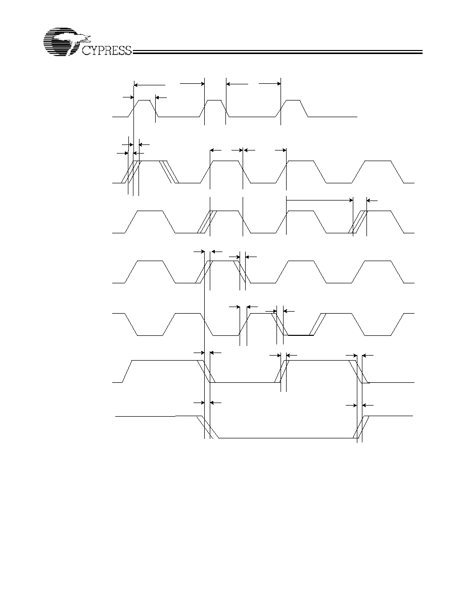
AC Timing Definitions
t
REF
t
0DCV
t
0DCV
t
PD
t
CCJ1-12
t
SKEWPR
t
SKEW0,1
t
SKEWPR
t
SKEW0,1
t
SKEW1
t
SKEW1
t
SKEW3
t
SKEW3
t
SKEW3
t
SKEW1,3,4
t
SKEW1,3,4
t
PWH
t
PWL
REF
FB
Q
OTHER Q
INVERTED Q
REF DIVIDED BY 2
REF DIVIDED BY 4
CY7B995
Document #: 38-07337 Rev. *A
Page 9 of 11
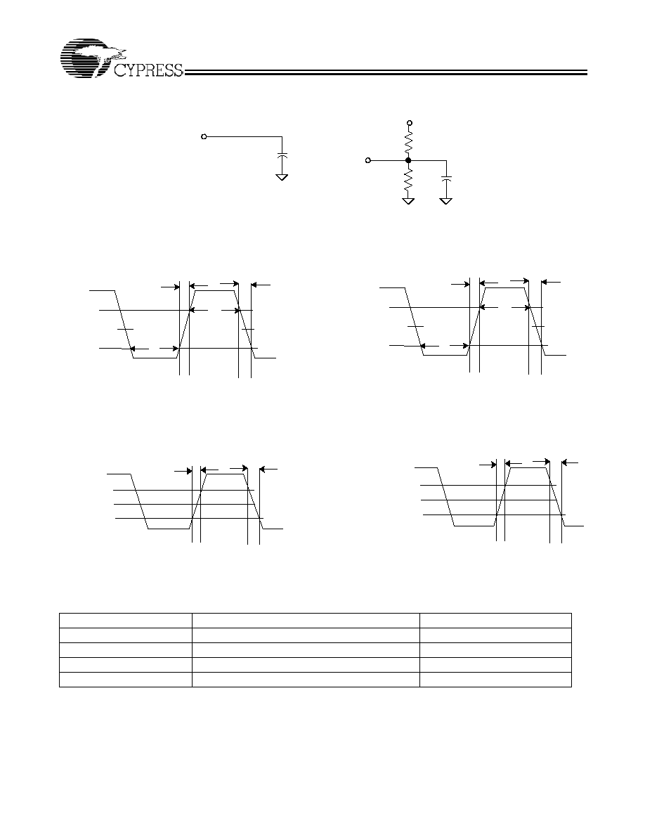
AC TEST LOADS AND WAVEFORMS
Output
20pF
Output
20pF
150
150
VDDQ
For Lock Output
For All Other Outputs
Figure 1.
2.0V
0.8V
VTH =1.5V
t
PWL
t
PWH
t
ORISE
t
OFALL
3.3V LVTTL OUTPUT WAVEFORM
2.5V LVTTL OUTPUT WAVEFORM
1.7V
0.7V
VTH =1.25V
t
PWL
t
PWH
t
ORISE
t
OFALL
Figure 2.
2.0V
0.8V
VTH =1.5V
1ns
1ns
3.0V
0V
3.3V LVTTL INPUT TEST WAVEFORM
1.7V
0.7V
VTH =1.25V
1ns
1ns
2.5V
0V
2.5V LVTTL INPUT TEST WAVEFORM
Figure 3.
Ordering Information
Part Number
Package Type
Product Flow
CY7B995AC
44 TQFP
Commercial, 0
° to 70°C
CY7B995ACT
44 TQFP Tape and Reel
Commercial, 0
° to 70°C
CY7B995AI
44 TQFP
Industrial, 40
° to 85°C
CY7B995AIT
44 TQFP Tape and Reel
Industrial, 40
° to 85°C
CY7B995
Document #: 38-07337 Rev. *A
Page 10 of 11
© Cypress Semiconductor Corporation, 2004. The information contained herein is subject to change without notice. Cypress Semiconductor Corporation assumes no responsibility for the use
of any circuitry other than circuitry embodied in a Cypress Semiconductor product. Nor does it convey or imply any license under patent or other rights. Cypress Semiconductor does not authorize
its products for use as critical components in life-support systems where a malfunction or failure may reasonably be expected to result in significant injury to the user. The inclusion of Cypress
Semiconductor products in life-support systems application implies that the manufacturer assumes all risk of such use and in doing so indemnifies Cypress Semiconductor against all charges.
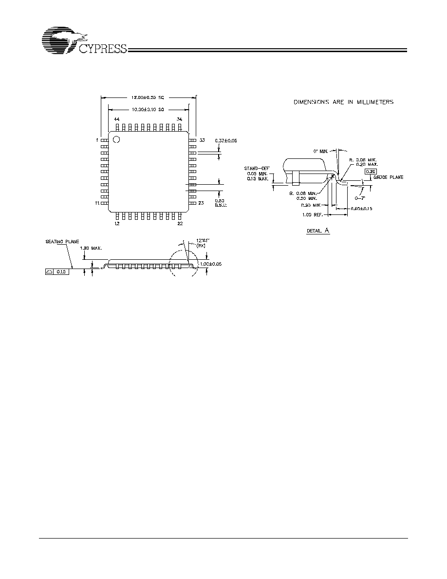
Package Drawing and Dimension
RoboClock is a registered trademark of Cypress Semiconductor. All product and company names mentioned in this document
are the trademarks of their respective holders.
44-lead Thin Plastic Quad Flat Pack (10 x 10 x 1.0 mm) A44SB
51-85155*A
CY7B995
Document #: 38-07337 Rev. *A
Page 11 of 11
Document History Page
Document Title:CY7B995 Roboclock
®
2.5/3.3V 200-MHz High-speed Multi-phase PLL Clock Buffer
Document Number: 38-07337
REV.
ECN No.
Issue Date
Orig. of
Change
Description of Change
**
122626
01/10/03
RGL
New Data Sheet
*A
205743
See ECN
RGL
Changed Pin 5 from VDD to VDDQ4, Pin 16 from VDD to VDDQ3 and Pin
29 from VDD to VDDQ1
Added pin 1 indicator in the Pin Configuration Drawing