4K x 16/18 and 8K x 16/18 Dual-Port
Static RAM with SEM, INT, BUSY
CY7C024/0241
CY7C025/0251
Cypress Semiconductor Corporation
∑
3901 North First Street
∑
San Jose
∑
CA 95134
∑
408-943-2600
Document #: 38-06035 Rev. *B
Revised June 22, 2004
Features
∑ True Dual-Ported memory cells which allow
simultaneous reads of the same memory location
∑ 4K x 16 organization (CY7C024)
∑ 4K x 18 organization (CY7C0241)
∑ 8K x 16 organization (CY7C025)
∑ 8K x 18 organization (CY7C0251)
∑ 0.65-micron CMOS for optimum speed/power
∑ High-speed access: 15 ns
∑ Low operating power: I
CC
= 150 mA (typ.)
∑ Fully asynchronous operation
∑ Automatic power-down
∑ Expandable data bus to 32/36 bits or more using
Master/Slave chip select when using more than one
device
∑ On-chip arbitration logic
∑ Semaphores included to permit software handshaking
between ports
∑ INT flag for port-to-port communication
∑ Separate upper-byte and lower-byte control
∑ Pin select for Master or Slave
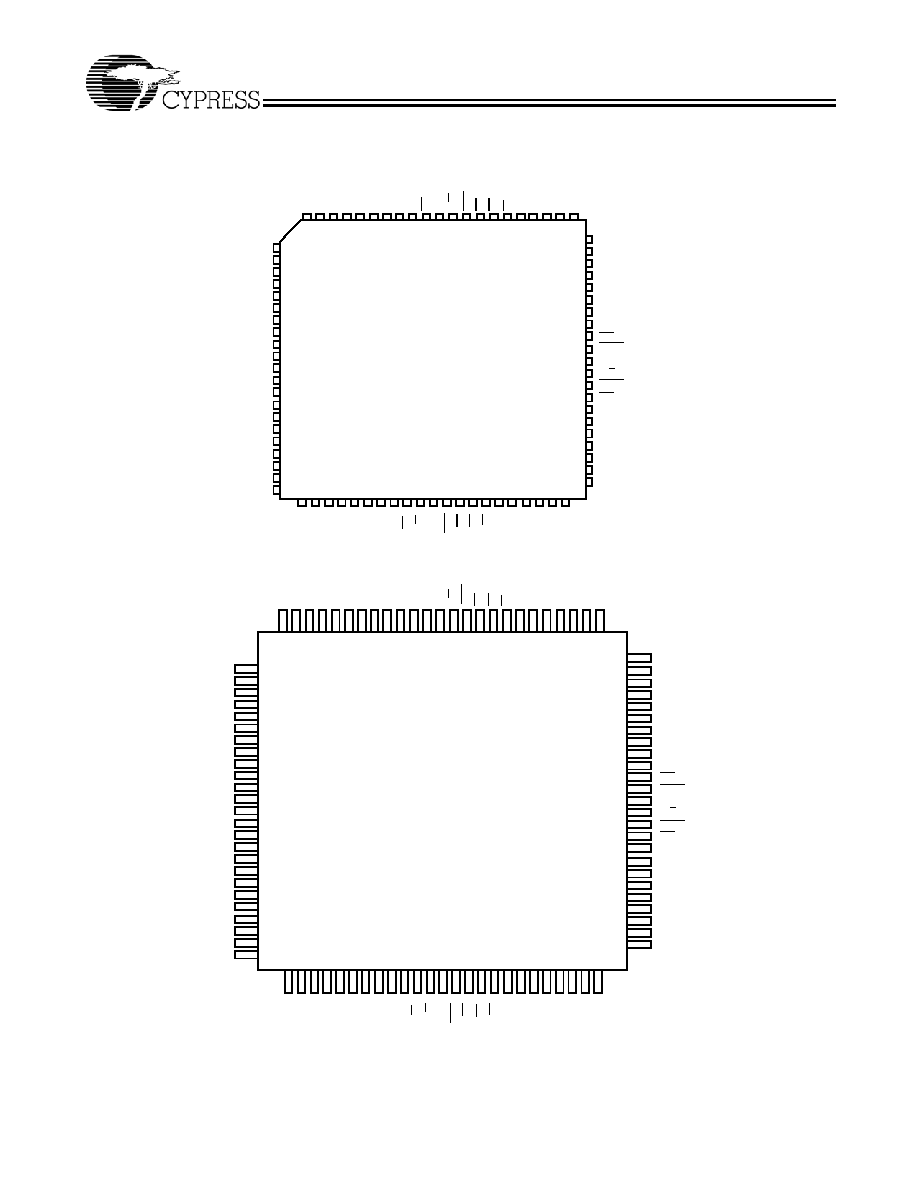
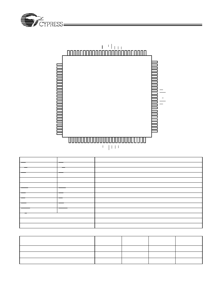
∑ Available in 84-pin PLCC and 100-pin TQFP
Functional Description
The CY7C024/0241 and CY7C025/0251 are low-power
CMOS 4K x 16/18 and 8K x 16/18 dual-port static RAMs. Var-
ious arbitration schemes are included on the CY7C024/0241
and CY7C025/0251 to handle situations when multiple pro-
cessors access the same piece of data. Two ports are provid-
ed, permitting independent, asynchronous access for reads
and writes to any location in memory. The CY7C024/0241 and
CY7C025/0251 can be utilized as standalone 16-/18-bit du-
al-port static RAMs or multiple devices can be combined in
order to function as a 32-/36-bit or wider master/slave du-
al-port static RAM. An M/S pin is provided for implementing
32-/36-bit or wider memory applications without the need for
separate master and slave devices or additional discrete logic.
Application areas include interprocessor/multiprocessor de-
signs, communications status buffering, and dual-port vid-
eo/graphics memory.
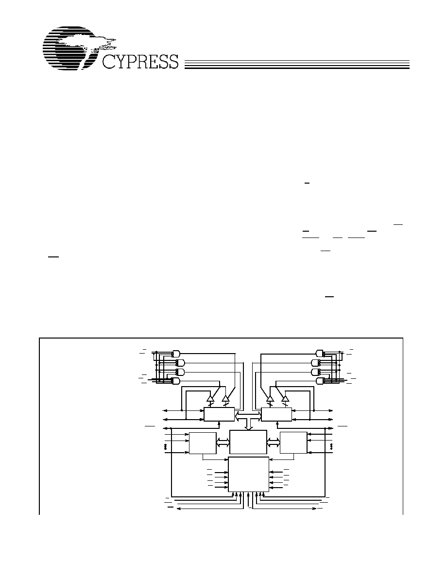
Each port has independent control pins: Chip Enable (CE),
Read or Write Enable (R/W), and Output Enable (OE). Two flags
are provided on each port (BUSY and INT). BUSY signals that the
port is trying to access the same location currently being accessed by
the other port. The Interrupt Flag (INT) permits communication be-
tween ports or systems by means of a mail box. The semaphores are
used to pass a flag, or token, from one port to the other to indicate that
a shared resource is in use. The semaphore logic is comprised of
eight shared latches. Only one side can control the latch (semaphore)
at any time. Control of a semaphore indicates that a shared resource
is in use. An automatic power-down feature is controlled indepen-
dently on each port by a chip select (CE) pin.
The CY7C024/0241 and CY7C025/0251 are available in
84-pin PLCCs (CY7C024 and CY7C025 only) and 100-pin
Thin Quad Plastic Flatpack (TQFP).
v
7C024≠1
R/W
L
UB
L
LB
L
CE
L
OE
L
A
0L
R/W
R
UB
R
CE
R
OE
R
CE
L
OE
L
UB
L
UB
R
I/O
8L
≠ I/O
15L
INTERRUPT
SEMAPHORE
ARBITRATION
CONTROL
I/O
MEMORY
ARRAY
ADDRESS
DECODER
SEM
L
SEM
R
BUSY
L
INT
L
INTR
M/S
CONTROL
I/O
LB
L
LB
R
I/O
0L
≠ I/O
7L
R/W
L
R/W
R
LB
R
CE
R
OE
R
A
0R
I/O
8R
I/O
15R
BUSY
R
I/O
0R
I/O
7R
(CY7C025/0251)
A
12L
A
12R
(CY7C025/0251)
[1]
[1]
Logic Block Diagram
≠
≠
ADDRESS
DECODER
A
11L
A
11R
[2]
[3]
[2]
[3]
CY7C024/0241
CY7C025/0251
Document #: 38-06035 Rev. *B
Page 5 of 20
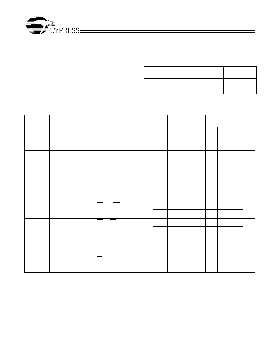
Maximum Ratings
[6]
(Above which the useful life may be impaired. For user guide-
lines, not tested.)
Storage Temperature .................................≠65
∞
C to +150
∞
C
Ambient Temperature with
Power Applied.............................................≠55
∞
C to +125
∞
C
Supply Voltage to Ground Potential ............... ≠0.3V to +7.0V
DC Voltage Applied to Outputs
in High Z State ............................................... ≠0.5V to +7.0V
DC Input Voltage
[7]
......................................... ≠0.5V to +7.0V
Output Current into Outputs (LOW) .............................20 mA
Static Discharge Voltage........................................... >2001V
(per MIL-STD-883, Method 3015)
Latch-Up Current.................................................... >200 mA
Operating Range
Range
Ambient
Temperature
V
CC
Commercial
0
∞
C to +70
∞
C
5V
±
10%
Industrial
≠40
∞
C to +85
∞
C
5V
±
10%
Electrical Characteristics
Over the Operating Range
Parameter
Description
Test Conditions
7C024/0241≠15
7C025/0251≠15
7C024/0241≠25
7C025/0251≠25
Unit
Min. Typ. Max. Min. Typ. Max.
V
OH
Output HIGH Voltage
V
CC
= Min., I
OH
= ≠4.0 mA
2.4
2.4
V
V
OL
Output LOW Voltage
V
CC
= Min., I
OL
= 4.0 mA
0.4
0.4
V
V
IH
Input HIGH Voltage
2.2
2.2
V
V
IL
Input LOW Voltage
≠0.7
0.8
≠0.7
0.8
V
I
IX
Input Leakage Current GND
V
I
V
CC
≠10
+10
≠10
+10
µ
A
I
OZ
Output Leakage
Current
Output Disabled,
GND
V
O
V
CC
≠10
+10
≠10
+10
µ
A
I
CC
Operating Current
V
CC
= Max., I
OUT
= 0 mA,
Outputs Disabled
Com'l
190
300
170
250
mA
Ind
200
320
170
290
I
SB1
Standby Current
(Both Ports TTL Lev-
els)
CE
L
and CE
R
V
IH
,
f = f
MAX
[8]
Com'l
50
70
40
60
mA
Ind
50
70
75
I
SB2
Standby Current
(One Port TTL Level)
CE
L
or CE
R
V
IH
,
f = f
MAX
[8]
Com'l
120
180
100
150
mA
Ind
120
180
100
170
I
SB3
Standby Current
(Both Ports CMOS
Levels)
Both Ports CE and CE
R
V
CC
≠ 0.2V, V
IN
V
CC
≠ 0.2V
or V
IN
0.2V, f = 0
[8]
Com'l
3
15
3
15
mA
Ind
3
15
3
15
I
SB4
Standby Current
(Both Ports CMOS
Levels)
One Port CE
L
or
CE
R
V
CC
≠ 0.2V,
V
IN
V
CC
≠ 0.2V or V
IN
0.2V,
Active Port Outputs, f = f
MAX
[8]
Com'l
110
160
90
130
mA
Ind
110
160
90
150
Notes:
6.
The Voltage on any input or sI/O pin cannot exceed the power pin during power-up
7.
Pulse width < 20 ns.
8.
f
MAX
= 1/t
RC
= All inputs cycling at f = 1/t
RC
(except output enable). f = 0 means no address or control lines change. This applies only to inputs at CMOS level standby I
SB3
.