/home/web/htmldatasheet/RUSSIAN/html/cypress/169413
16K x 16/18 Dual-Port Static RAM
CY7C026A
CY7C036A
Cypress Semiconductor Corporation
·
3901 North First Street
·
San Jose
·
CA 95134
·
408-943-2600
Document #: 38-06046 Rev. *A
Revised December 27, 2002
25/0251
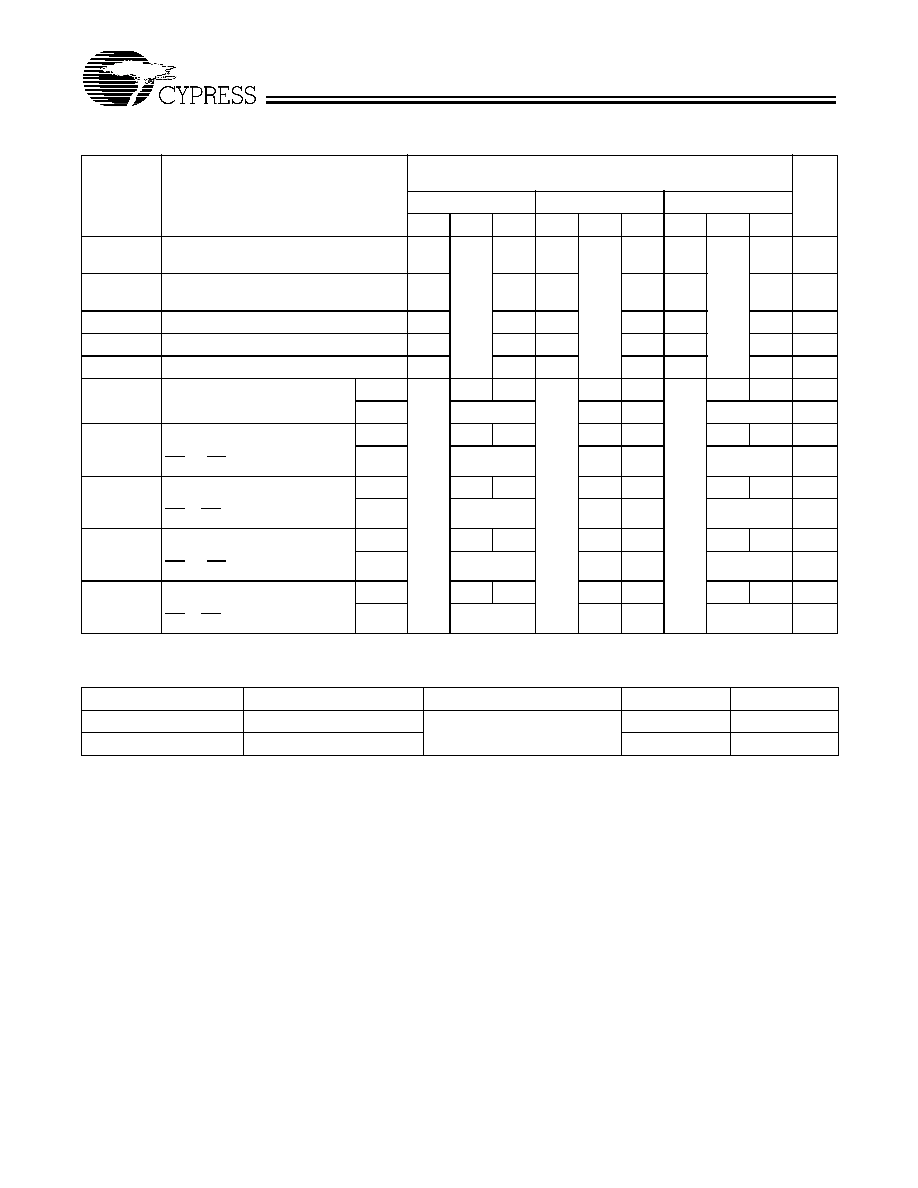
Features
· True dual-ported memory cells which allow simulta-
neous access of the same memory location
· 16K x 16 organization (CY7C026A)
· 16K x 18 organization (CY7C036A)
· 0.35-micron CMOS for optimum speed/power
· High-speed access: 12
[1]
/15/20 ns
· Low operating power
-- Active: I
CC
= 180 mA (typical)
-- Standby: I
SB3
= 0.05 mA (typical)
· Fully asynchronous operation
· Automatic power-down
· Expandable data bus to 32/36 bits or more using Mas-
ter/Slave chip select when using more than one device
· On-chip arbitration logic
· Semaphores included to permit software handshaking
between ports
· INT flags for port-to-port communication
· Separate upper-byte and lower-byte control
· Pin select for Master or Slave
· Commercial and Industrial temperature ranges
· Available in 100-Pin TQFP
· Pin-compatible and functionally equivalent to IDT70261
Notes:
1.
See page 6 for Load Conditions.
2.
I/O
8
I/O
15
for x16 devices; I/O
9
I/O
17
for x18 devices.
3.
I/O
0
I/O
7
for x16 devices; I/O
0
I/O
8
for x18 devices.
4.
BUSY is an output in master mode and an input in slave mode.
R/W
L
OE
L
I/O
8/9L
I/O
15/17L
I/O
Control
Address
Decode
A
0L
A
13L
CE
L
OE
L
R/W
L
BUSY
L
I/O
Control
CE
L
Interrupt
Semaphore
Arbitration
SEM
L
INT
L
M/S
UB
L
LB
L
I/O
0L
I/O
7/8L
R/W
R
OE
R
I/O
8/9L
I/O
15/17R
CE
R
UB
R
LB
R
I/O
0L
I/O
7/8R
UB
L
LB
L
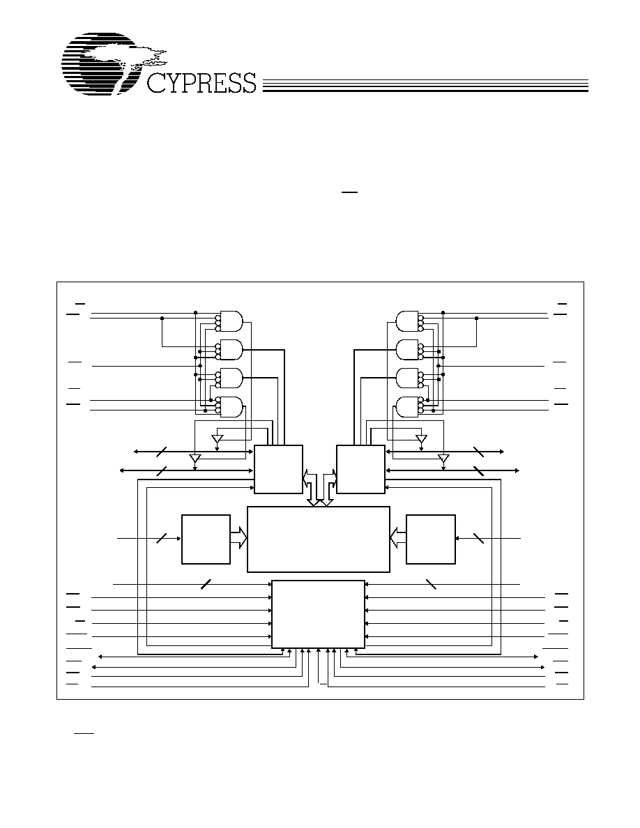
Logic Block Diagram
A
0L
A
13L
True Dual-Ported
RAM Array
A
0R
A
13R
CE
R
OE
R
R/W
R
BUSY
R
SEM
R
INT
R
UB
R
LB
R
Address
Decode
A
0R
A
13R
[2]
[2]
[3]
[3]
[4]
[4]
14
8/9
8/9
14
8/9
8/9
14
14
For the most recent information, visit the Cypress web site at www.cypress.com
CY7C026A
CY7C036A
Document #: 38-06046 Rev. *A
Page 2 of 18
Functional Description
The CY7C026A and CY7C036A are low-power CMOS 16K x
16/18 dual-port static RAMs. Various arbitration schemes are
included on the devices to handle situations when multiple pro-
cessors access the same piece of data. Two ports are provid-
ed, permitting independent, asynchronous access for reads
and writes to any location in memory. The devices can be uti-
lized as standalone 16/18-bit dual-port static RAMs or multiple
devices can be combined in order to function as a 32/36-bit or
wider master/slave dual-port static RAM. An M/S pin is provid-
ed for implementing 32/36-bit or wider memory applications
without the need for separate master and slave devices or
additional discrete logic. Application areas include interpro-
cessor/multiprocessor designs, communications status buffer-
ing, and dual-port video/graphics memory.
Each port has independent control pins: Chip Enable (CE),
Read or Write Enable (R/W), and Output Enable (OE). Two
flags are provided on each port (BUSY and INT). BUSY sig-
nals that the port is trying to access the same location currently
being accessed by the other port. The Interrupt flag (INT) per-
mits communication between ports or systems by means of a
mail box. The semaphores are used to pass a flag, or token,
from one port to the other to indicate that a shared resource is
in use. The semaphore logic is comprised of eight shared
latches. Only one side can control the latch (semaphore) at
any time. Control of a semaphore indicates that a shared re-
source is in use. An automatic power-down feature is con-
trolled independently on each port by the chip enable pin.
The CY7C026A and CY7C036A are available in 100-pin Thin
Quad Plastic Flatpack (TQFP) packages.
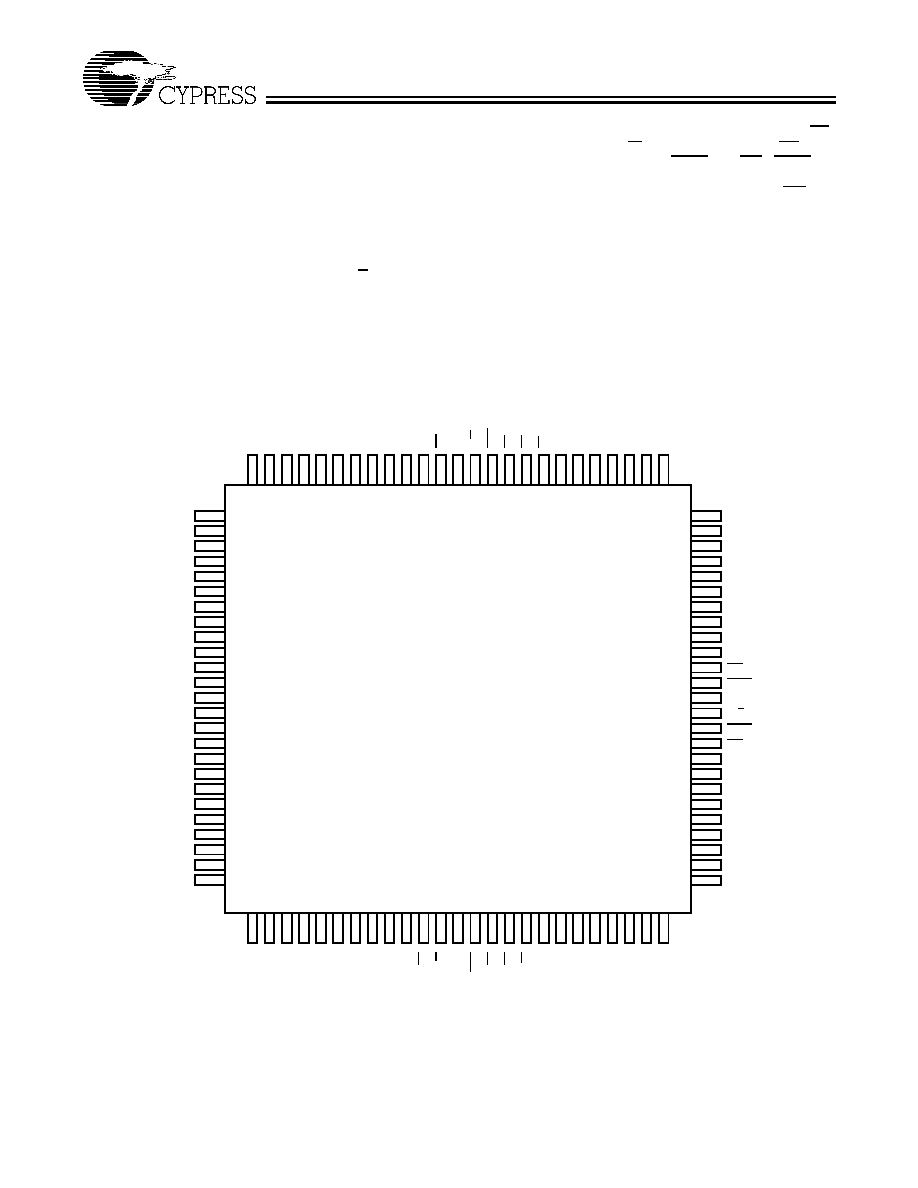
Pin Configurations
100-Pin TQFP (Top View)
1
3
2
92 91 90
84
85
87 86
88
89
83 82 81
76
78 77
79
80
93
94
95
96
97
98
99
100
59
60
61
67
66
64
65
63
62
68
69
70
75
73
74
72
71
NC
NC
NC
A
6L
A
5L
A
4L
INT
L
A
2L
A
0L
GND
M/S
A
0R
A
1R
A
1L
A
3L
BUSY
R
INT
R
A
2R
A
3R
A
4R
A
5R
NC
NC
NC
BUSY
L
58
57
56
55
54
53
52
51
CY7C026A (16K x 16)
NC
NC
NC
NC
I/O
10L
I/O
11L
I/O
15L
I/O
13L
I/O
14L
GND
I/O
0R
VCC
I/O
3R
GND
I/O
12L
I/O
1R
I/O
2R
I/O
4R
I/O
5R
I/O
6R
NC
NC
NC
NC
VCC
17
16
15
9
10
12
11
13
14
8
7
6
4
5
18
19
20
21
22
23
24
25
I/O
9L
I/O
8L
I/O
7L
I/O
6L
I/O
5L
I/O
4L
I/O
0L
I/O
2L
I/O
1L
VCC
R/W
L
UB
L
LB
L
GND
I/O
3L
SE
M
L
CE
L
A
13
L
A
12
L
A
11
L
A
10
L
A
9L
A
8L
A
7L
OE
L
34 35 36
42
41
39 40
38
37
43 44 45
50
48 49
47
46
A
6R
A
7R
A
8R
A
9R
A
10R
A
11
R
CE
R
A
13R
UB
R
GND
R/W
R
GND
I/O
14R
LB
R
A
12R
OE
R
I/O
15R
I/O
13R
I/O
12R
I/O
11
R
I/O
10R
I/O
9R
I/O
8R
I/O
7R
SE
M
R
33
32
31
30
29
28
27
26
CY7C026A
CY7C036A
Document #: 38-06046 Rev. *A
Page 3 of 18
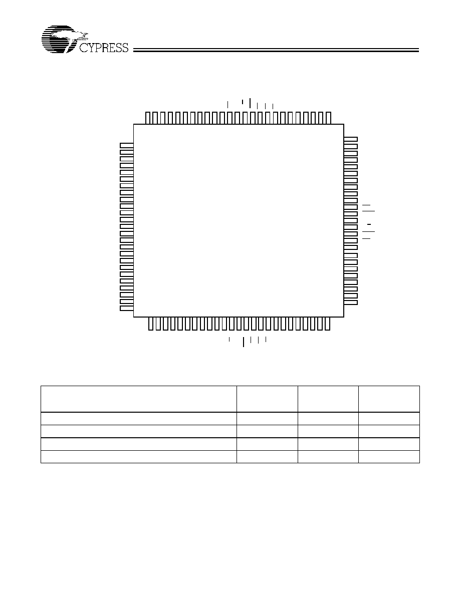
Pin Configurations
(continued)
Selection Guide
CY7C026A
CY7C036A
-12
[1]
CY7C026A
CY7C036A
-15
CY7C026A
CY7C036A
-20
Maximum Access Time (ns)
12
15
20
Typical Operating Current (mA)
195
190
180
Typical Standby Current for I
SB1
(mA) (Both Ports TTL Level)
55
50
45
Typical Standby Current for I
SB3
(mA) (Both Ports CMOS Level)
0.05
0.05
0.05
Top View
100-Pin TQFP
100 99
97
98
96
2
3
1
42
41
59
60
61
12
13
15
14
16
4
5
40
39
95 94
17
26
9
10
8
7
6
11
27 28
30
29
31 32
35
34
36 37 38
33
67
66
64
65
63
62
68
69
70
75
73
74
72
71
89 88
86
87
85
93 92
84
NC
NC
NC
A
5L
A
4L
INT
L
A
2L
A
0L
BUSY
L
GND
INT
R
A
0R
A
1L
NC
NC
I/O
11L
I/O
12L
I/O
16L
V
CC
GND
I/O
1R
I/O
2R
V
CC
90
91
A
3L
M/S
BUSY
R
I/O
15L
GND
I/O
13L
I/O
14L
A
1R
A
2R
A
3R
A
4R
NC
NC
NC
I/O
3R
I/O
4R
I/O
5R
I/O
6R
NC
NC
18
19
20
21
22
23
24
25
83 82 81 80 79 78 77 76
58
57
56
55
54
53
52
51
43 44 45 46 47 48 49 50
I/O
9L
I/O
7L
I/O
6L
I/O
5L
I/O
4L
I/O
3L
I/O
2L
I/O
10
L
GND
I/O
1L
I/O
0L
OE
L
SE
M
L
V
CC
CE
L
UB
L
LB
L
A
11
L
A
10L
A
9L
A
8L
A
7L
A
6L
I/O
0R
I/O
7R
I/O
16R
I/O
9R
I/O
10R
I/O
11
R
I/O
12R
I/O
13R
I/O
14R
GN
D
I/O
15R
OE
R
R/W
R
GN
D
SE
M
R
CE
R
UB
R
LB
R
A
11
R
A
10R
A
9R
A
8R
A
7R
A
6R
A
5R
I/O
8L
I/O
17L
I/O
8R
I/O
17R
R/W
L
CY7C036A (16K x 18)
A
13L
A
13R
A
12L
A
12
R
CY7C026A
CY7C036A
Document #: 38-06046 Rev. *A
Page 4 of 18
Maximum Ratings
[5]
(Above which the useful life may be impaired. For user guide-
lines, not tested.)
Storage Temperature .................................65
°
C to +150
°
C
Ambient Temperature with
Power Applied.............................................55
°
C to +125
°
C
Supply Voltage to Ground Potential ............... 0.3V to +7.0V
DC Voltage Applied to Outputs
in High Z State ............................................... 0.5V to +7.0V
DC Input Voltage
[6]
........................................0.5V to + 7.0V
Output Current into Outputs (LOW)............................. 20 mA
Static Discharge Voltage........................................... >2001V
Latch-Up Current .................................................... >200 mA
Note:
5.
The Voltage on any input or I/O pin cannot exceed the power pin during power-up.
6.
Pulse width < 20 ns.
Pin Definitions
Left Port
Right Port
Description
CE
L
CE
R
Chip Enable
R/W
L
R/W
R
Read/Write Enable
OE
L
OE
R
Output Enable
A
0L
A
13L
A
0R
A
13R
Address
I/O
0L
I/O
17L
I/O
0R
I/O
17R
Data Bus Input/Output
SEM
L
SEM
R
Semaphore Enable
UB
L
UB
R
Upper Byte Select (I/O
8
I/O
15
for x16 devices; I/O
9
I/O
17
for x18 devices)
LB
L
LB
R
Lower Byte Select (I/O
0
I/O
7
for x16 devices; I/O
0
I/O
8
for x18 devices)
INT
L
INT
R
Interrupt Flag
BUSY
L
BUSY
R
Busy Flag
M/S
Master or Slave Select
V
CC
Power
GND
Ground
NC
No Connect
Operating Range
Range
Ambient
Temperature
V
CC
Commercial
0
°
C to +70
°
C
5V
±
10%
Industrial
40
°
C to +85
°
C 5V
±
10%
CY7C026A
CY7C036A
Document #: 38-06046 Rev. *A
Page 5 of 18
Notes:
7.
f
MAX
= 1/t
RC
= All inputs cycling at f = 1/t
RC
(except output enable). f = 0 means no address or control lines change. This applies only to inputs at CMOS level
standby I
SB3
.
8.
Tested initially and after any design or process changes that may affect these parameters.
Electrical Characteristics
Over the Operating Range
Parameter
Description
CY7C026A
CY7C036A
Unit
-12
[1]
-15
-20
Min.
Typ.
Max.
Min.
Typ.
Max.
Min.
Typ.
Max.
V
OH
Output HIGH Voltage (V
CC
=Min., I
OH
=
4.0 mA)
2.4
2.4
2.4
V
V
OL
Output LOW Voltage (V
CC
=Min., I
OH
=
+4.0 mA)
0.4
0.4
0.4
V
V
IH
Input HIGH Voltage
2.2
2.2
2.2
V
V
IL
Input LOW Voltage
0.8
0.8
0.8
V
I
OZ
Output Leakage Current
10
10
10
10
10
10
µ
A
I
CC
Operating Current (V
CC
= Max.,
I
OUT
= 0 mA) Outputs Disabled
Com'l.
195
325
190
285
180
275
mA
Indust.
215
305
mA
I
SB1
Standby Current
(Both Ports TTL Level)
CE
L
& CE
R
V
IH
, f = f
MAX
Com'l.
55
75
50
70
45
65
mA
Indust.
65
95
mA
I
SB2
Standby Current
(One Port TTL Level)
CE
L
| CE
R
V
IH
, f = f
MAX
Com'l.
125
205
120
180
110
160
mA
Indust.
135
205
mA
I
SB3
Standby Current
(Both Ports CMOS Level)
CE
L
& CE
R
V
CC
0.2V, f = 0
Com'l.
0.05
0.5
0.05
0.5
0.05
0.5
mA
Indust.
0.05
0.5
mA
I
SB4
Standby Current
(One Port CMOS Level)
CE
L
| CE
R
V
IH
, f = f
MAX
[7]
Com'l.
115
185
110
160
100
140
mA
Indust.
125
175
mA
Capacitance
[8]
Parameter
Description
Test Conditions
Max.
Unit
C
IN
Input Capacitance
T
A
= 25
°
C, f = 1 MHz,
V
CC
= 5.0V
10
pF
C
OUT
Output Capacitance
10
pF
CY7C026A
CY7C036A
Document #: 38-06046 Rev. *A
Page 6 of 18
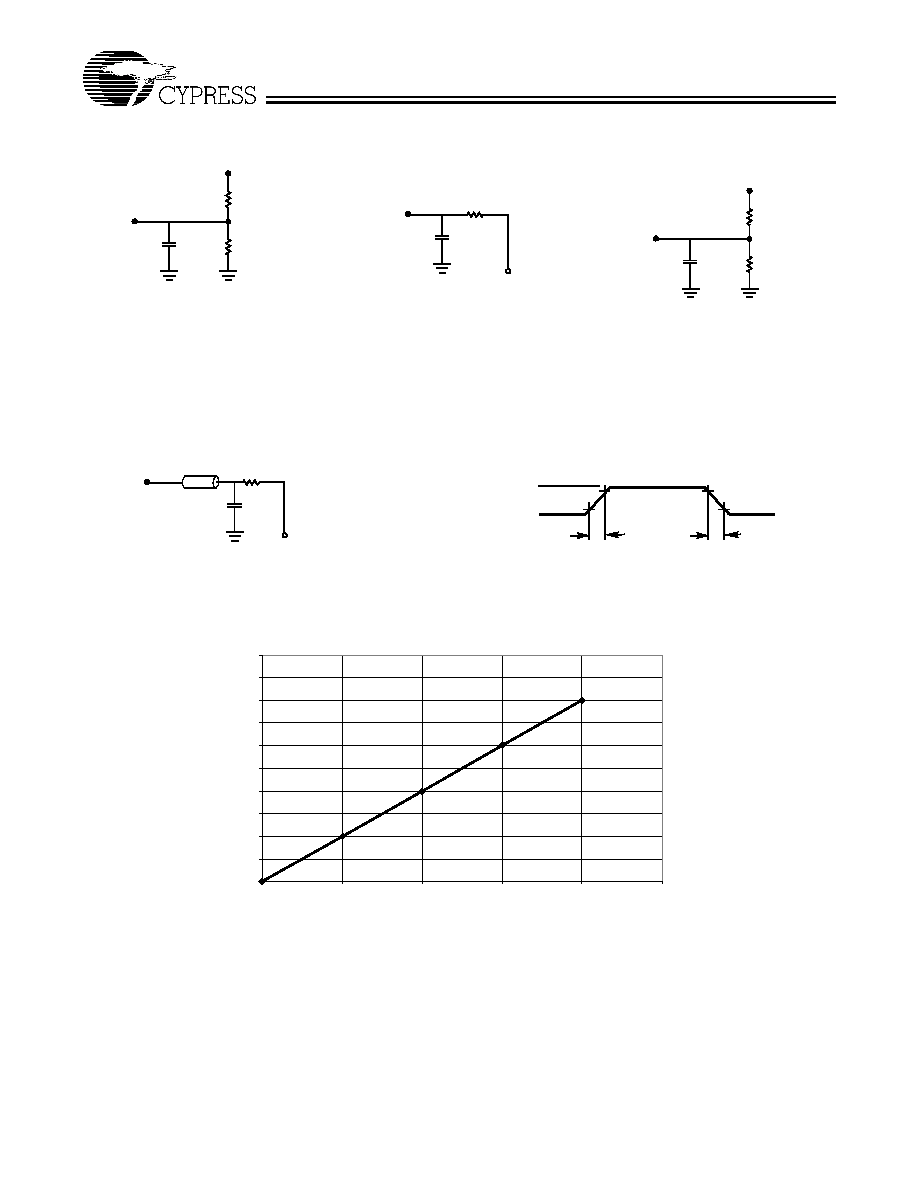
AC Test Loads (Applicable to -12 only)
[9]
Note:
9.
Test Conditions: C = 10 pF.
AC Test Loads and Waveforms
(a) Normal Load (Load 1)
R1 = 893
5V
OUTPUT
R2 = 347
C = 30 pF
V
TH
= 1.4V
OUTPUT
C = 30 pF
(b) Thévenin Equivalent (Load 1)
(c) Three-State Delay (Load 2)
R1 = 893
R2 = 347
5V
OUTPUT
C = 5 pF
R
TH
= 250
(Used for t
LZ
, t
HZ
, t
HZWE
, & t
LZWE
including scope and jig)
V
TH
= 1.4V
OUTPUT
C
(a) Load 1 (-12 only)
R = 50
Z
0
= 50
3.0V
GND
90%
90%
10%
3 ns
3 ns
10%
ALL INPUT PULSES
0. 00
0. 1 0
0. 20
0. 30
0. 40
0. 50
0. 60
0. 70
0. 80
0. 90
1 . 00
1 0
1 5
20
25
30
35
(b) Load Derating Curve
Capacitance (pF)
(ns
)
for
al
l
-
12 a
cces
s
ti
mes
CY7C026A
CY7C036A
Document #: 38-06046 Rev. *A
Page 7 of 18
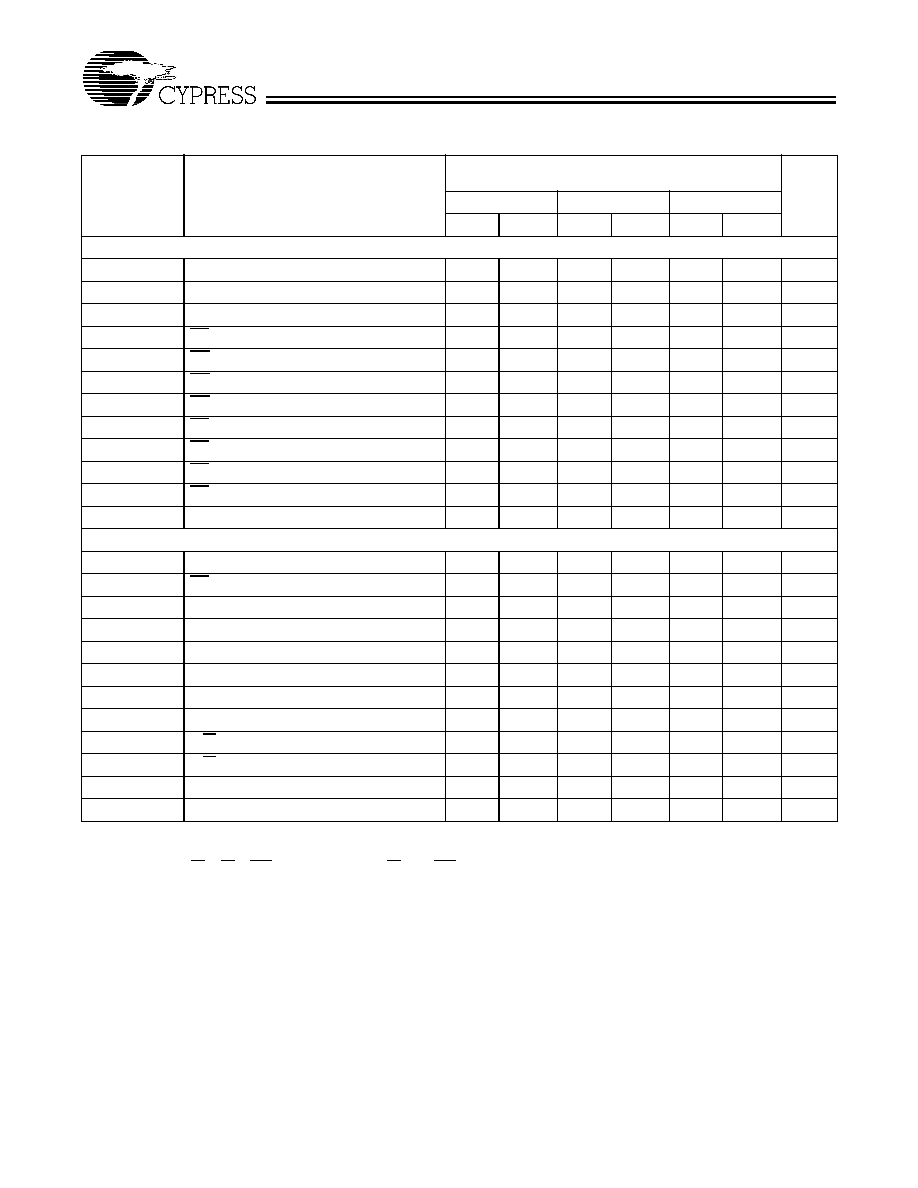
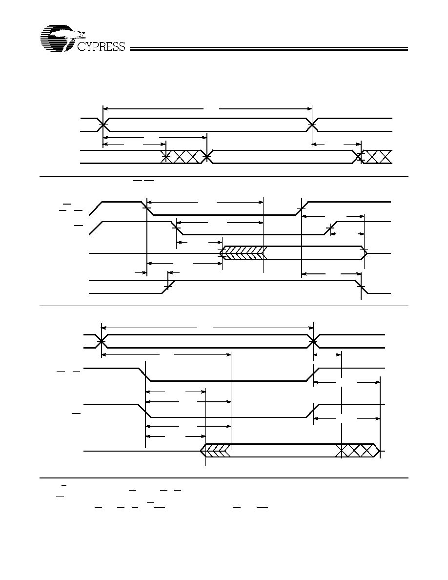
Switching Characteristics
Over the Operating Range
[10]
Parameter
Description
CY7C026A
CY7C036A
Unit
-12
[1]
-15
-20
Min.
Max.
Min.
Max.
Min.
Max.
READ CYCLE
t
RC
Read Cycle Time
12
15
20
ns
t
AA
Address to Data Valid
12
15
20
ns
t
OHA
Output Hold From Address Change
3
3
3
ns
t
ACE
[11]
CE LOW to Data Valid
12
15
20
ns
t
DOE
OE LOW to Data Valid
8
10
12
ns
t
LZOE
[12, 13, 14]
OE LOW to Low Z
3
3
3
ns
t
HZOE
[12, 13, 14]
OE HIGH to High Z
10
10
12
ns
t
LZCE
[12, 13, 14]
CE LOW to Low Z
3
3
3
ns
t
HZCE
[12, 13, 14]
CE HIGH to High Z
10
10
12
ns
t
PU
[14]
CE LOW to Power-Up
0
0
0
ns
t
PD
[14]
CE HIGH to Power-Down
12
15
20
ns
t
ABE
[11]
Byte Enable Access Time
12
15
20
ns
WRITE CYCLE
t
WC
Write Cycle Time
12
15
20
ns
t
SCE
[11]
CE LOW to Write End
10
12
15
ns
t
AW
Address Valid to Write End
10
12
15
ns
t
HA
Address Hold From Write End
0
0
0
ns
t
SA
[11]
Address Set-Up to Write Start
0
0
0
ns
t
PWE
Write Pulse Width
10
12
15
ns
t
SD
Data Set-Up to Write End
10
10
15
ns
t
HD
[16]
Data Hold From Write End
0
0
0
ns
t
HZWE
[13, 14]
R/W LOW to High Z
10
10
12
ns
t
LZWE
[13, 14]
R/W HIGH to Low Z
3
3
3
ns
t
WDD
[15]
Write Pulse to Data Delay
25
30
45
ns
t
DDD
[15]
Write Data Valid to Read Data Valid
20
25
30
ns
Notes:
10. Test conditions assume signal transition time of 3 ns or less, timing reference levels of 1.5V, input pulse levels of 0 to 3.0V, and output loading of the specified
I
OI
/I
OH
and 30-pF load capacitance.
11.
To access RAM, CE=L, UB=L, SEM=H. To access semaphore, CE=H and SEM=L. Either condition must be valid for the entire t
SCE
time.
12. At any given temperature and voltage condition for any given device, t
HZCE
is less than t
LZCE
and t
HZOE
is less than t
LZOE
.
13. Test conditions used are Load 3.
14. This parameter is guaranteed but not tested.
15. For information on port-to-port delay through RAM cells from writing port to reading port, refer to Read Timing with Busy waveform.
16. For 15 ns industrial parts t
HD
Min. is 0.5 ns.
CY7C026A
CY7C036A
Document #: 38-06046 Rev. *A
Page 8 of 18
Data Retention Mode
The CY7C026A and CY7C036A are designed with battery
backup in mind. Data retention voltage and supply current are
guaranteed over temperature. The following rules ensure data
retention:
1. Chip Enable (CE) must be held HIGH during data retention, with-
in V
CC
to V
CC
0.2V.
2. CE must be kept between V
CC
0.2V and 70% of V
CC
during the power-up and power-down transitions.
3. The RAM can begin operation >t
RC
after V
CC
reaches the
minimum operating voltage (4.5 volts).
Notes:
17. Test conditions used are Load 2.
18. t
BDD
is a calculated parameter and is the greater of t
WDD
t
PWE
(actual) or t
DDD
t
SD
(actual).
19. CE = V
CC
, V
in
= GND to V
CC
, T
A
= 25
°
C. This parameter is guaranteed but not tested.
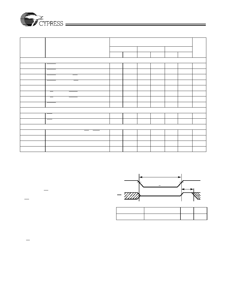
BUSY TIMING
[17]
t
BLA
BUSY LOW from Address Match
12
15
20
ns
t
BHA
BUSY HIGH from Address Mismatch
12
15
20
ns
t
BLC
BUSY LOW from CE LOW
12
15
20
ns
t
BHC
BUSY HIGH from CE HIGH
12
15
17
ns
t
PS
Port Set-Up for Priority
5
5
5
ns
t
WB
R/W HIGH after BUSY (Slave)
0
0
0
ns
t
WH
R/W HIGH after BUSY HIGH (Slave)
11
13
15
ns
t
BDD
[18]
BUSY HIGH to Data Valid
12
15
20
ns
INTERRUPT TIMING
[17]
t
INS
INT Set Time
12
15
20
ns
t
INR
INT Reset Time
12
15
20
ns
SEMAPHORE TIMING
t
SOP
SEM Flag Update Pulse (OE or SEM)
10
10
10
ns
t
SWRD
SEM Flag Write to Read Time
5
5
5
ns
t
SPS
SEM Flag Contention Window
5
5
5
ns
t
SAA
SEM Address Access Time
12
15
20
ns
Switching Characteristics
Over the Operating Range
[10]
(continued)
Parameter
Description
CY7C026A
CY7C036A
Unit
-12
[1]
-15
-20
Min.
Max.
Min.
Max.
Min.
Max.
Timing
Parameter
Test Conditions
[19]
Max.
Unit
ICC
DR1
@ VCC
DR
= 2V
1.5
mA
Data Retention Mode
4.5V
4.5V
V
CC
>
2.0V
V
CC
to V
CC
0.2V
V
CC
CE
t
RC
V
IH
CY7C026A
CY7C036A
Document #: 38-06046 Rev. *A
Page 9 of 18
Switching Waveforms
Notes:
20. R/W is HIGH for read cycles.
21. Device is continuously selected CE = V
IL
and UB or LB = V
IL
. This waveform cannot be used for semaphore reads.
22. OE = V
IL
.
23. Address valid prior to or coincident with CE transition LOW.
24. To access RAM, CE = V
IL
, UB or LB = V
IL
, SEM = V
IH
. To access semaphore, CE = V
IH
, SEM = V
IL
.
t
RC
t
AA
t
OHA
DATA VALID
PREVIOUS DATA VALID
DATA OUT
ADDRESS
t
OHA
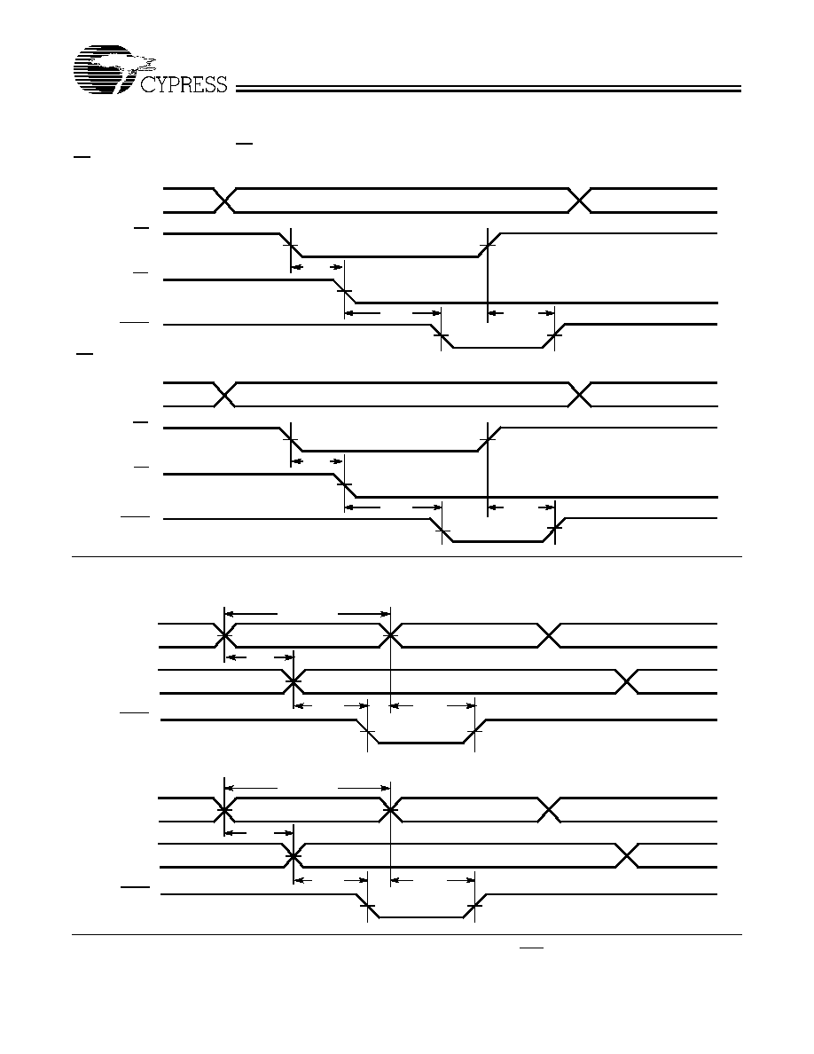
Read Cycle No.1 (Either Port Address Access)
[20, 21, 22]
t
ACE
t
LZOE
t
DOE
t
HZOE
t
HZCE
DATA VALID
t
LZCE
t
PU
t
PD
I
SB
I
CC
DATA OUT
OE
CE and
LB or UB
CURRENT
Read Cycle No.2 (Either Port CE/OE Access)
[20, 23, 24]
UB or LB
DATA OUT
t
RC
ADDRESS
t
AA
t
OHA
CE
t
LZCE
t
ABE
t
HZCE
t
HZCE
t
ACE
t
LZCE
Read Cycle No. 3 (Either Port)
[20, 22, 23, 24]
CY7C026A
CY7C036A
Document #: 38-06046 Rev. *A
Page 10 of 18
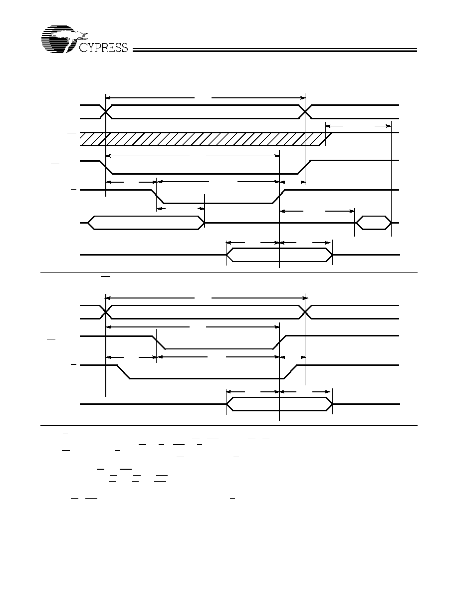
Notes:
25. R/W must be HIGH during all address transitions.
26. A write occurs during the overlap (t
SCE
or t
PWE
) of a LOW CE or SEM and a LOW UB or LB.
27. t
HA
is measured from the earlier of CE or R/W or (SEM or R/W) going HIGH at the end of write cycle.
28. If OE is LOW during a R/W controlled write cycle, the write pulse width must be the larger of t
PWE
or (t
HZWE
+ t
SD
) to allow the I/O drivers to turn off and
data to be placed on the bus for the required t
SD
. If OE is HIGH during an R/W controlled write cycle, this requirement does not apply and the write pulse
can be as short as the specified t
PWE
.
29. To access RAM, CE = V
IL
, SEM = V
IH
.
30. To access upper byte, CE = V
IL
, UB = V
IL
, SEM = V
IH
.
To access lower byte, CE = V
IL
, LB = V
IL
, SEM = V
IH
.
31. Transition is measured
±
500 mV from steady state with a 5-pF load (including scope and jig). This parameter is sampled and not 100% tested.
32. During this period, the I/O pins are in the output state, and input signals must not be applied.
33. If the CE or SEM LOW transition occurs simultaneously with or after the R/W LOW transition, the outputs remain in the high-impedance state.
Switching Waveforms
(continued)
t
AW
t
WC
t
PWE
t
HD
t
SD
t
HA
CE
R/W
OE
DATA OUT
DATA IN
ADDRESS
t
HZOE
t
SA
t
HZWE
t
LZWE
Write Cycle No. 1: R/W Controlled Timing
[25, 26, 27, 28]
[31]
[31]
[28]
[29,30]
NOTE 32
NOTE 32
t
AW
t
WC
t
SCE
t
HD
t
SD
t
HA
CE
R/W
DATA IN
ADDRESS
t
SA
Write Cycle No. 2: CE Controlled Timing
[25, 26, 27, 33]
[29,30]
CY7C026A
CY7C036A
Document #: 38-06046 Rev. *A
Page 11 of 18
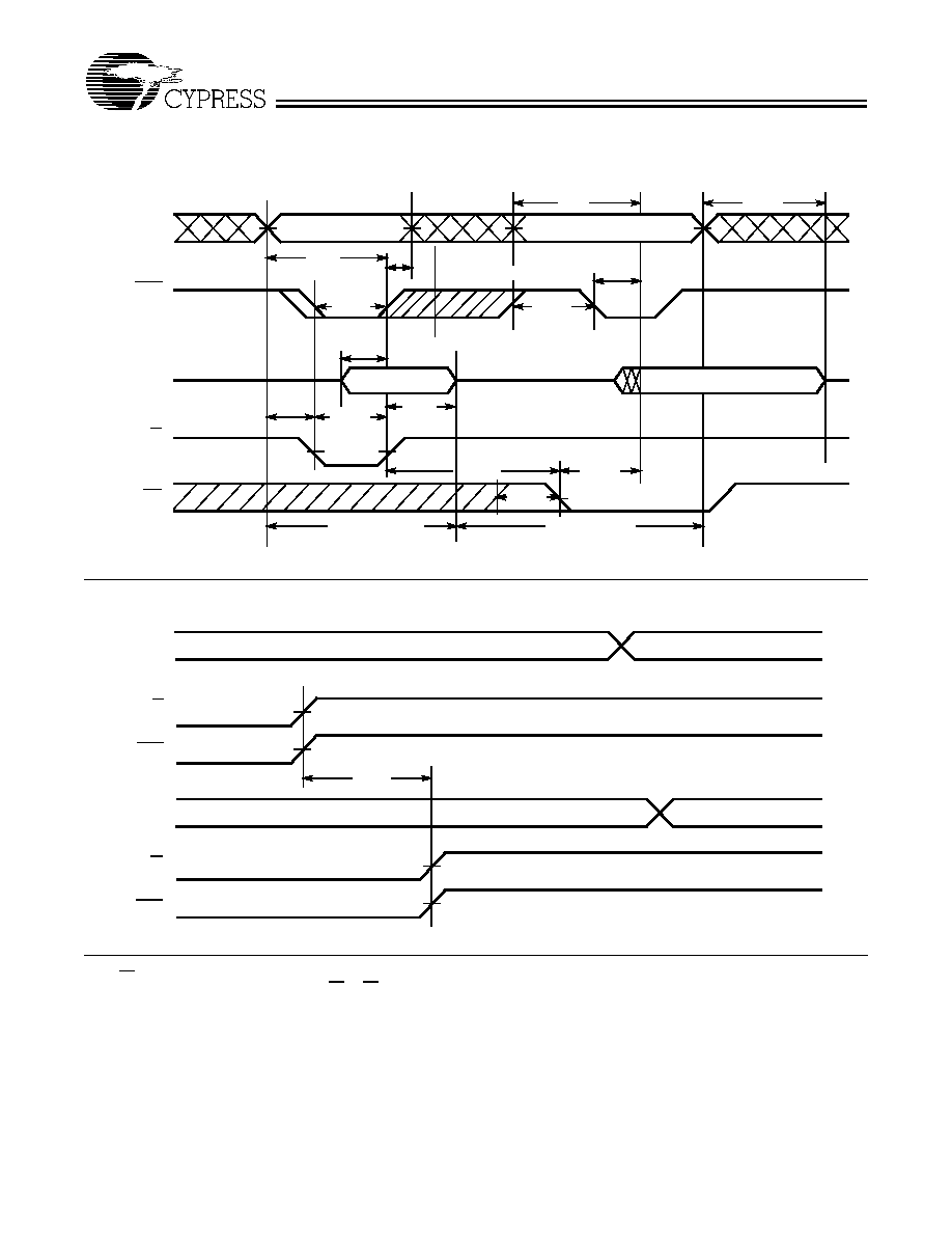
Notes:
34. CE = HIGH for the duration of the above timing (both write and read cycle).
35. I/O
0R
= I/O
0L
= LOW (request semaphore); CE
R
= CE
L
= HIGH.
36. Semaphores are reset (available to both ports) at cycle start.
37. If t
SPS
is violated, the semaphore will definitely be obtained by one side or the other, but which side will get the semaphore is unpredictable.
Switching Waveforms
(continued)
t
SOP
t
SAA
VALID ADRESS
VALID ADRESS
t
HD
DATA
IN
VALID
DATA
OUT
VALID
t
OHA
t
AW
t
HA
t
ACE
t
SOP
t
SCE
t
SD
t
SA
t
PWE
t
SWRD
t
DOE
WRITE CYCLE
READ CYCLE
OE
R/W
I/O
0
SEM
A
0
A
2
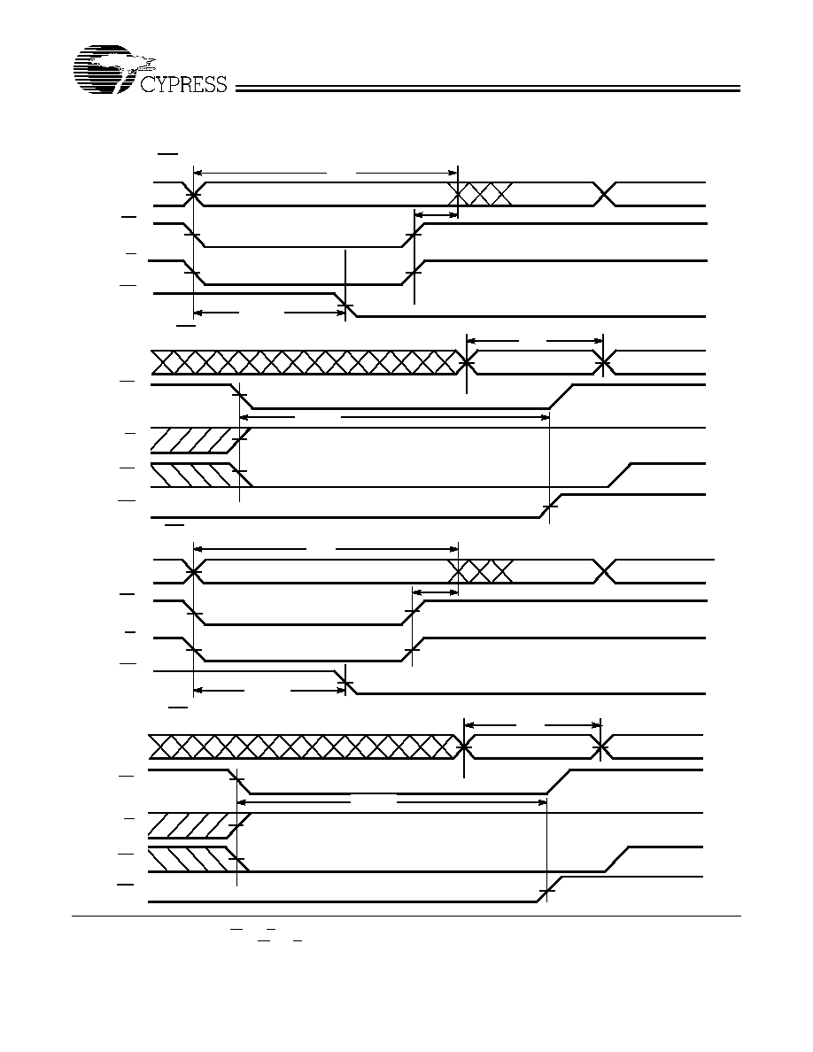
Semaphore Read After Write Timing, Either Side
[34]
MATCH
t
SPS
A
0L
A
2L
MATCH
R/W
L
SEM
L
A
0R
A
2R
R/W
R
SEM
R
Timing Diagram of Semaphore Contention
[35, 36, 37]
CY7C026A
CY7C036A
Document #: 38-06046 Rev. *A
Page 12 of 18
Note:
38. CE
L
= CE
R
= LOW.
Switching Waveforms
(continued)
VALID
t
DDD
t
WDD
MATCH
MATCH
R/W
R
DATA IN
R
DATA
OUTL
t
WC
ADDRESS
R
t
PWE
VALID
t
SD
t
HD
ADDRESS
L
t
PS
t
BLA
t
BHA
t
BDD
BUSY
L
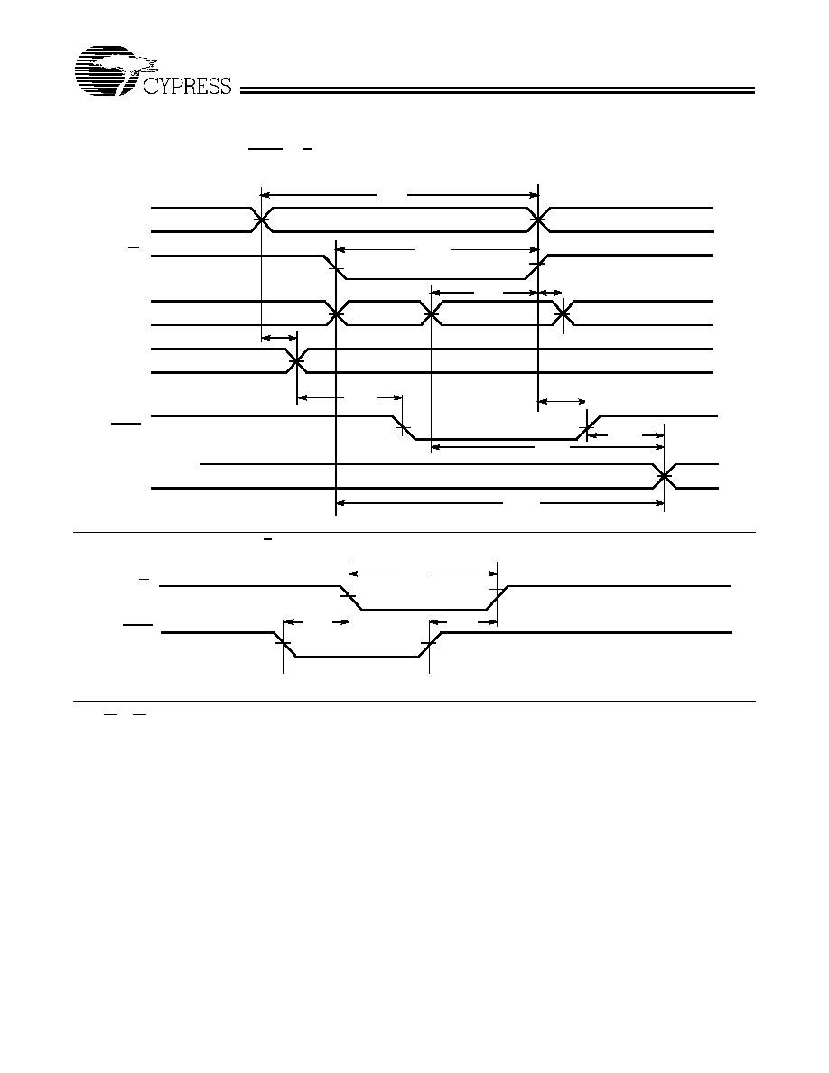
Timing Diagram of Read with BUSY (M/S=HIGH)
[38]
t
PWE
R/W
BUSY
t
WB
t
WH
Write Timing with Busy Input (M/S=LOW)
CY7C026A
CY7C036A
Document #: 38-06046 Rev. *A
Page 13 of 18
Note:
39. If t
PS
is violated, the busy signal will be asserted on one side or the other, but there is no guarantee to which side BUSY will be asserted.
Switching Waveforms
(continued)
ADDRESS MATCH
t
PS
t
BLC
t
BHC
ADDRESS MATCH
t
PS
t
BLC
t
BHC
CE
R
Valid First:
ADDRESS
L,R
BUSY
R
CE
L
CE
R
BUSY
L
CE
R
CE
L
ADDRESS
L,R
Busy Timing Diagram No. 1 (CE Arbitration)
[39]
CE
L
Valid First:
ADDRESS MATCH
t
PS
ADDRESS
L
BUSY
R
ADDRESS MISMATCH
t
RC
or t
WC
t
BLA
t
BHA
ADDRESS
R
ADDRESS MATCH
ADDRESS MISMATCH
t
PS
ADDRESS
L
BUSY
L
t
RC
or t
WC
t
BLA
t
BHA
ADDRESS
R
Right Address Valid First:
Busy Timing Diagram No. 2 (Address Arbitration)
[39]
Left Address Valid First:
CY7C026A
CY7C036A
Document #: 38-06046 Rev. *A
Page 14 of 18
Notes:
40. t
HA
depends on which enable pin (CE
L
or R/W
L
) is deasserted first.
41. t
INS
or t
INR
depends on which enable pin (CE
L
or R/W
L
) is asserted last.
Switching Waveforms
(continued)
Interrupt Timing Diagrams
WRITE 3FFF
t
WC
Right Side Clears INT
R
:
t
HA
READ 3FFF
t
RC
t
INR
WRITE 3FFE
t
WC
Right Side Sets INT
L
:
Left Side Sets INT
R
:
Left Side Clears INT
L
:
READ 3FFE
t
INR
t
RC
ADDRESS
R
CE
L
R/W
L
INT
L
OE
L
ADDRESS
R
R/W
R
CE
R
INT
L
ADDRESS
R
CE
R
R/W
R
INT
R
OE
R
ADDRESS
L
R/W
L
CE
L
INT
R
t
INS
t
HA
t
INS
[40]
[41]
[41]
[41]
[40]
[41]

CY7C026A
CY7C036A
Document #: 38-06046 Rev. *A
Page 15 of 18
Architecture
The CY7C026A and CY7C036A consist of an array of 16K
words of 16 and 18 bits each of dual-port RAM cells, I/O and
address lines, and control signals (CE, OE, R/W). These con-
trol pins permit independent access for reads or writes to any
location in memory. To handle simultaneous writes/reads to
the same location, a BUSY pin is provided on each port. Two
Interrupt (INT) pins can be utilized for port-to-port communica-
tion. Two Semaphore (SEM) control pins are used for allocat-
ing shared resources. With the M/S pin, the devices can func-
tion as a master (BUSY pins are outputs) or as a slave (BUSY
pins are inputs). The devices also have an automatic power-
down feature controlled by CE. Each port is provided with its
own Output Enable control (OE), which allows data to be read
from the device.
Functional Description
Write Operation
Data must be set up for a duration of t
SD
before the rising edge
of R/W in order to guarantee a valid write. A write operation is
controlled by either the R/W pin (see Write Cycle No. 1 wave-
form) or the CE pin (see Write Cycle No. 2 waveform). Re-
quired inputs for non-contention operations are summarized in
Table 1.
If a location is being written to by one port and the opposite
port attempts to read that location, a port-to-port flowthrough
delay must occur before the data is read on the output; other-
wise the data read is not deterministic. Data will be valid on the
port t
DDD
after the data is presented on the other port.
Read Operation
When reading the device, the user must assert both the OE
and CE pins. Data will be available t
ACE
after CE or t
DOE
after
OE is asserted. If the user wishes to access a semaphore flag,
then the SEM pin must be asserted instead of the CE pin, and
OE must also be asserted.
Interrupts
The upper two memory locations may be used for message
passing. The highest memory location (3FFF) is the mailbox
for the right port and the second-highest memory location
(3FFE) is the mailbox for the left port. When one port writes to
the other port's mailbox, an interrupt is generated to the owner.
The interrupt is reset when the owner reads the contents of the
mailbox. The message is user defined.
Each port can read the other port's mailbox without resetting
the interrupt. The active state of the busy signal (to a port)
prevents the port from setting the interrupt to the winning port.
Also, an active busy to a port prevents that port from reading
its own mailbox and, thus, resetting the interrupt to it.
If an application does not require message passing, do not
connect the interrupt pin to the processor's interrupt request
input pin.
The operation of the interrupts and their interaction with Busy
are summarized in Table 2.
Busy
The CY7C026A and CY7C036A provide on-chip arbitration to
resolve simultaneous memory location access (contention). If
both ports' CEs are asserted and an address match occurs
within t
PS
of each other, the busy logic will determine which
port has access. If t
PS
is violated, one port will definitely gain
permission to the location, but it is not predictable which port
will get that permission. BUSY will be asserted t
BLA
after an
address match or t
BLC
after CE is taken LOW.
Master/Slave
A M/S pin is provided in order to expand the word width by
configuring the device as either a master or a slave. The BUSY
output of the master is connected to the BUSY input of the
slave. This will allow the device to interface to a master device
with no external components. Writing to slave devices must be
delayed until after the BUSY input has settled (t
BLC
or t
BLA
),
otherwise, the slave chip may begin a write cycle during a
contention situation. When tied HIGH, the M/S pin allows the
device to be used as a master and, therefore, the BUSY line
is an output. BUSY can then be used to send the arbitration
outcome to a slave.
Semaphore Operation
The CY7C026A and CY7C036A provide eight semaphore
latches, which are separate from the dual-port memory loca-
tions. Semaphores are used to reserve resources that are
shared between the two ports. The state of the semaphore
indicates that a resource is in use. For example, if the left port
wants to request a given resource, it sets a latch by writing a
zero to a semaphore location. The left port then verifies its
success in setting the latch by reading it. After writing to the
semaphore, SEM or OE must be deasserted for t
SOP
before
attempting to read the semaphore. The semaphore value will
be available t
SWRD
+ t
DOE
after the rising edge of the sema-
phore write. If the left port was successful (reads a zero), it
assumes control of the shared resource, otherwise (reads a
one) it assumes the right port has control and continues to poll
the semaphore. When the right side has relinquished control
of the semaphore (by writing a one), the left side will succeed
in gaining control of the semaphore. If the left side no longer
requires the semaphore, a one is written to cancel its request.
Semaphores are accessed by asserting SEM LOW. The SEM
pin functions as a chip select for the semaphore latches (CE
must remain HIGH during SEM LOW). A
02
represents the
semaphore address. OE and R/W are used in the same man-
ner as a normal memory access. When writing or reading a
semaphore, the other address pins have no effect.
When writing to the semaphore, only I/O
0
is used. If a zero is
written to the left port of an available semaphore, a one will
appear at the same semaphore address on the right port. That
semaphore can now only be modified by the side showing zero
(the left port in this case). If the left port now relinquishes con-
trol by writing a one to the semaphore, the semaphore will be
set to one for both sides. However, if the right port had request-
ed the semaphore (written a zero) while the left port had con-
trol, the right port would immediately own the semaphore as
soon as the left port released it. Table 3 shows sample sema-
phore operations.
When reading a semaphore, all sixteen/eighteen data lines
output the semaphore value. The read value is latched in an
output register to prevent the semaphore from changing state
during a write from the other port. If both ports attempt to ac-
cess the semaphore within t
SPS
of each other, the semaphore
will definitely be obtained by one side or the other, but there is
no guarantee which side will control the semaphore.
CY7C026A
CY7C036A
Document #: 38-06046 Rev. *A
Page 16 of 18
Table 1. Non-Contending Read/Write
Inputs
Outputs
CE
R/W
OE
UB
LB
SEM
I/O
9
I/O
17
I/O
0
I/O
8
Operation
H
X
X
X
X
H
High Z
High Z
Deselected: Power-Down
X
X
X
H
H
H
High Z
High Z
Deselected: Power-Down
L
L
X
L
H
H
Data In
High Z
Write to Upper Byte Only
L
L
X
H
L
H
High Z
Data In
Write to Lower Byte Only
L
L
X
L
L
H
Data In
Data In
Write to Both Bytes
L
H
L
L
H
H
Data Out
High Z
Read Upper Byte Only
L
H
L
H
L
H
High Z
Data Out
Read Lower Byte Only
L
H
L
L
L
H
Data Out
Data Out
Read Both Bytes
X
X
H
X
X
X
High Z
High Z
Outputs Disabled
H
H
L
X
X
L
Data Out
Data Out
Read Data in Semaphore Flag
X
H
L
H
H
L
Data Out
Data Out
Read Data in Semaphore Flag
H
X
X
X
L
Data In
Data In
Write D
IN0
into Semaphore Flag
X
X
H
H
L
Data In
Data In
Write D
IN0
into Semaphore Flag
L
X
X
L
X
L
Not Allowed
L
X
X
X
L
L
Not Allowed
Table 2. Interrupt Operation Example (assumes BUSY
L
=BUSY
R
=HIGH)
Left Port
Right Port
Function
R/W
L
CE
L
OE
L
A
0L13L
INT
L
R/W
R
CE
R
OE
R
A
0R13R
INT
R
Set Right INT
R
Flag
L
L
X
3FFF
X
X
X
X
X
L
[43]
Reset Right INT
R
Flag
X
X
X
X
X
X
L
L
3FFF
H
[42]
Set Left INT
L
Flag
X
X
X
X
L
[42]
L
L
X
3FFE
X
Reset Left INT
L
Flag
X
L
L
3FFE
H
[43]
X
X
X
X
X
Table 3. Semaphore Operation Example
Function
I/O
0
I/O
17
Left
I/O
0
I/O
17
Right
Status
No action
1
1
Semaphore free
Left port writes 0 to semaphore
0
1
Left Port has semaphore token
Right port writes 0 to semaphore
0
1
No change. Right side has no write access to semaphore
Left port writes 1 to semaphore
1
0
Right port obtains semaphore token
Left port writes 0 to semaphore
1
0
No change. Left port has no write access to semaphore
Right port writes 1 to semaphore
0
1
Left port obtains semaphore token
Left port writes 1 to semaphore
1
1
Semaphore free
Right port writes 0 to semaphore
1
0
Right port has semaphore token
Right port writes 1 to semaphore
1
1
Semaphore free
Left port writes 0 to semaphore
0
1
Left port has semaphore token
Left port writes 1 to semaphore
1
1
Semaphore free
Notes:
42. If BUSY
L
=L, then no change.
43. If BUSY
R
=L, then no change.
CY7C026A
CY7C036A
Document #: 38-06046 Rev. *A
Page 17 of 18
© Cypress Semiconductor Corporation, 2001. The information contained herein is subject to change without notice. Cypress Semiconductor Corporation assumes no responsibility for the use
of any circuitry other than circuitry embodied in a Cypress Semiconductor product. Nor does it convey or imply any license under patent or other rights. Cypress Semiconductor does not authorize
its products for use as critical components in life-support systems where a malfunction or failure may reasonably be expected to result in significant injury to the user. The inclusion of Cypress
Semiconductor products in life-support systems application implies that the manufacturer assumes all risk of such use and in doing so indemnifies Cypress Semiconductor against all charges.
Ordering Information
16K x16 Asynchronous Dual-Port SRAM
Speed
(ns)
Ordering Code
Package
Name
Package Type
Operating
Range
12
[1]
CY7C026A-12AC
A100
100-Pin Thin Quad Flat Pack
Commercial
15
CY7C026A-15AC
A100
100-Pin Thin Quad Flat Pack
Commercial
CY7C026A-15AI
A100
100-Pin Thin Quad Flat Pack
Industrial
20
CY7C026A-20AC
A100
100-Pin Thin Quad Flat Pack
Commercial
16K x18 Asynchronous Dual-Port SRAM
Speed
(ns)
Ordering Code
Package
Name
Package Type
Operating
Range
12
[1]
CY7C036A-12AC
A100
100-Pin Thin Quad Flat Pack
Commercial
15
CY7C036A-15AC
A100
100-Pin Thin Quad Flat Pack
Commercial
CY7C036A-15AI
A100
100-Pin Thin Quad Flat Pack
Industrial
20
CY7C036A-20AC
A100
100-Pin Thin Quad Flat Pack
Commercial
Package Diagram
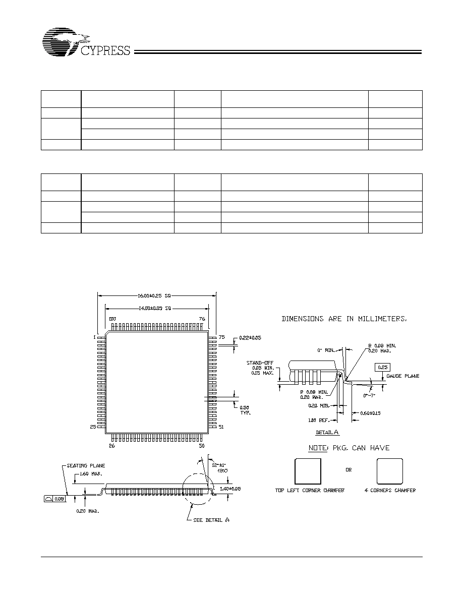
100-Pin Thin Plastic Quad Flat Pack (TQFP) A100
51-85048-B

CY7C026A
CY7C036A
Document #: 38-06046 Rev. *A
Page 18 of 18
Document Title: CY7C026A/CY7C036A 16K X 16/18 Dual-Port Static RAM
Document Number: 38-06046
REV.
ECN NO.
Issue
Date
Orig. of
Change
Description of Change
**
110198
09/29/01
SZV
Change from Spec number: 38-00832 to 38-06046
*A
122296
12/27/02
RBI
Power up requirements added to Maximum Ratings Information