3.3V 8K/16K x 9
Synchronous Dual Port Static RAM
CY7C09159AV
CY7C09169AV
Cypress Semiconductor Corporation
∑
3901 North First Street
∑
San Jose
∑
CA 95134
∑
408-943-2600
Document #: 38-06053 Rev. **
Revised September 21, 2001
25/0251
Features
∑ True Dual-Ported memory cells which allow simulta-
neous access of the same memory location
∑ Two Flow-Through/Pipelined devices
-- 8K x 9 organization (CY7C09159AV)
-- 16K x 9 organization (CY7C09169AV)
∑ Three Modes
-- Flow-Through
-- Pipelined
-- Burst
∑ Pipelined output mode on both ports allows fast 83-MHz
operation
∑ 0.35-micron CMOS for optimum speed/power
∑ High-speed clock to data access 9 and 12 ns (max.)
∑ 3.3V Low operating power
-- Active = 135 mA (typical)
-- Standby = 10
µ
A (typical)
∑ Fully synchronous interface for easier operation
∑ Burst counters increment addresses internally
-- Shorten cycle times
-- Minimize bus noise
-- Supported in Flow-Through and Pipelined modes
∑ Dual Chip Enables for easy depth expansion
∑ Automatic power-down
∑ Commercial and industrial temperature ranges
∑ Available in 100-pin TQFP
Notes:
1.
A
0
-
A
12
for 8K; A
0
-
A
13
for 16K.
v
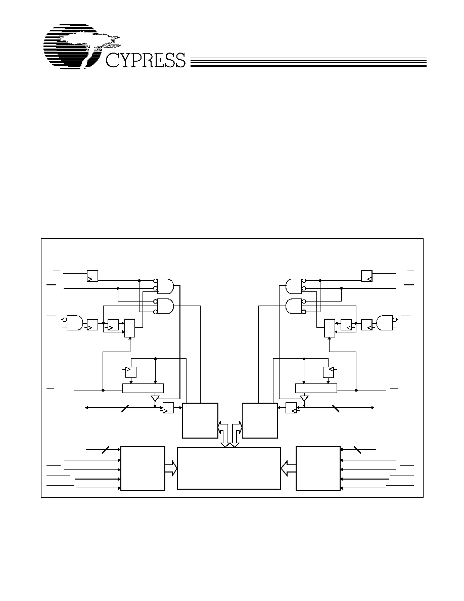
Logic Block Diagram
R/W
L
CE
0L
CE
1L
OE
L
FT/Pipe
L
I/O
0L
-
I/O
8L
Control
A
0
-
A
12/13L
CLK
L
ADS
L
CNTEN
L
CNTRST
L
R/W
R
1
0
0/1
CE
0R
CE
1R
OE
R
1
0/1
0
FT/Pipe
R
I/O
0R
-
I/O
8R
I/O
Control
A
0
-
A
12/13R
CLK
R
ADS
R
CNTEN
R
CNTRST
R
1
0
0/1
1
0/1
0
I/O
Counter/
Address
Register
Decode
True Dual-Ported
RAM Array
Counter/
Address
Register
Decode
9
9
[1]
[1]
13/14
13/14
For the most recent information, visit the Cypress web site at www.cypress.com
CY7C09159AV
CY7C09169AV
Document #: 38-06053 Rev. **
Page 2 of 17
Functional Description
The CY7C09159AV and CY7C09169AV are high-speed syn-
chronous CMOS 8K and 16K x 9 dual-port static RAMs. Two
ports are provided, permitting independent, simultaneous ac-
cess for reads and writes to any location in memory.
[2]
Regis-
ters on control, address, and data lines allow for minimal set-
up and hold times. In pipelined output mode, data is registered
for decreased cycle time. Clock to data valid t
CD2
= 9 ns (pipe-
lined). Flow-through mode can also be used to bypass the
pipelined output register to eliminate access latency. In flow-
through mode data will be available t
CD1
= 18 ns after the ad-
dress is clocked into the device. Pipelined output or flow-
through mode is selected via the FT/Pipe pin.
Each port contains a burst counter on the input address regis-
ter. The internal write pulse width is independent of the LOW-
to-HIGH transition of the clock signal. The internal write pulse
is self-timed to allow the shortest possible cycle times.
A HIGH on CE
0
or LOW on CE
1
for one clock cycle will power
down the internal circuitry to reduce the static power consump-
tion. The use of multiple Chip Enables allows easier banking
of multiple chips for depth expansion configurations. In the
pipelined mode, one cycle is required with CE
0
LOW and CE
1
HIGH to reactivate the outputs.
Counter enable inputs are provided to stall the operation of the
address input and utilize the internal address generated by the
internal counter for fast interleaved memory applications. A
port's burst counter is loaded with the port's Address Strobe
(ADS). When the port's Count Enable (CNTEN) is asserted,
the address counter will increment on each LOW-to-HIGH
transition of that port's clock signal. This will read/write one
word from/into each successive address location until CNTEN
is deasserted. The counter can address the entire memory
array and will loop back to the start. Counter Reset (CNTRST)
is used to reset the burst counter.
All parts are available in 100-pin Thin Quad Plastic Flatpack
(TQFP) packages.
Note:
2.
When simultaneously writing to the same location, final value cannot be guaranteed.
CY7C09159AV
CY7C09169AV
Document #: 38-06053 Rev. **
Page 3 of 17
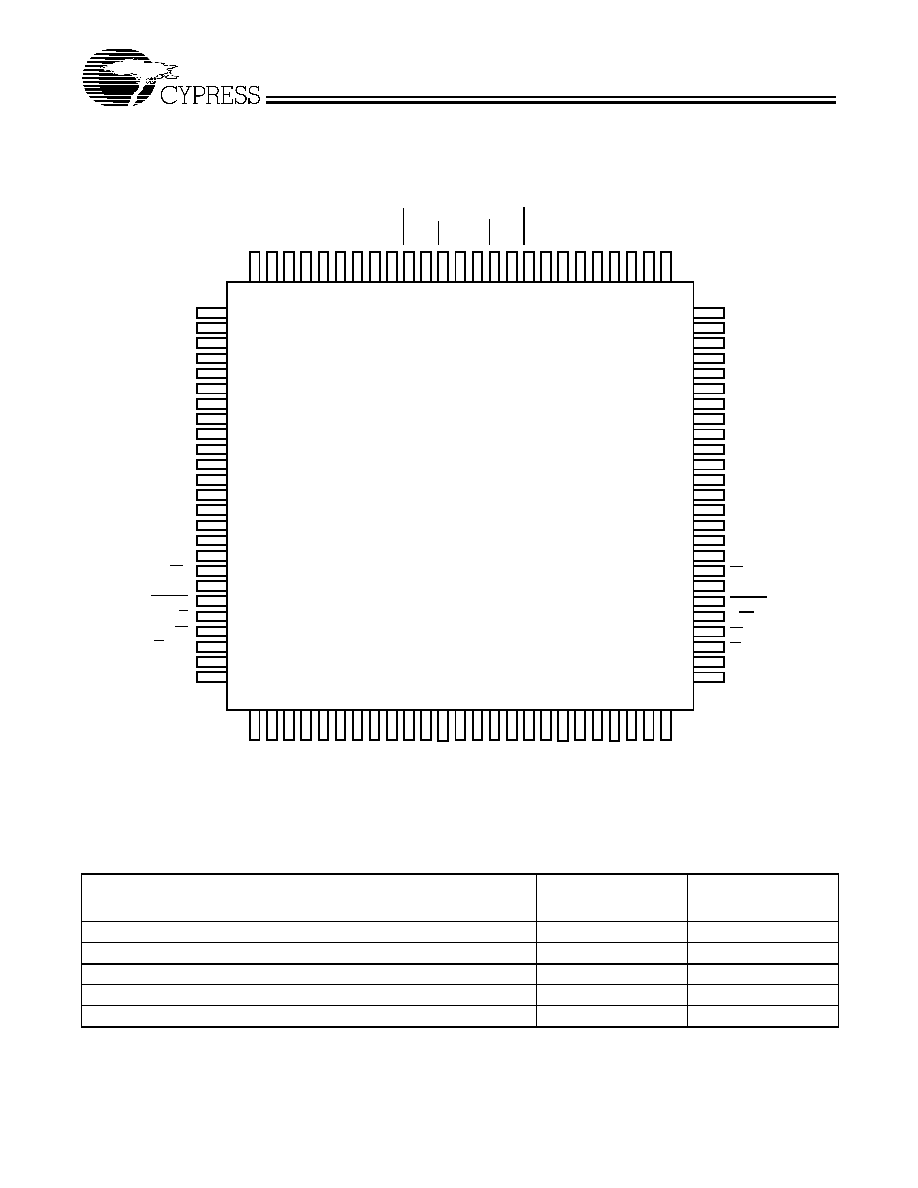
Pin Configuration
Note:
3.
This pin is NC for CY7C09159AV.
Selection Guide
CY7C09159AV
CY7C09169AV
-9
CY7C09159AV
CY7C09169AV
-12
f
MAX2
(MHz) (Pipelined)
67
50
Max Access Time (ns) (Clock to Data, Pipelined)
9
12
Typical Operating Current I
CC
(mA)
135
115
Typical Standby Current for I
SB1
(mA) (Both Ports TTL Level)
20
20
Typical Standby Current for I
SB3
(
µ
A) (Both Ports CMOS Level)
10
µ
A
10
µ
A
1
3
2
92 91 90
84
85
87 86
88
89
83 82 81
76
78 77
79
80
93
94
95
96
97
98
99
100
59
60
61
67
66
64
65
63
62
68
69
70
75
73
74
72
71
NC
NC
A7R
A8R
A9R
A10R
NC
A12R
NC
GND
NC
NC
CE0R
A13R
A11R
NC
NC
CE1R
CNTRSTR
R/WR
OER
FT/PIPER
GND
NC
NC
58
57
56
55
54
53
52
51
CY7C09159AV (8K x 9)
NC
NC
A7L
A8L
A9L
A10L
NC
A12L
NC
VCC
NC
NC
CE0L
A13L
A11L
NC
NC
CE1L
CNTRSTL
R/WL
OEL
FT/PIPEL
NC
NC
NC
17
16
15
9
10
12
11
13
14
8
7
6
4
5
18
19
20
21
22
23
24
25
NC
NC
A6
L
A5
L
A4
L
A3
L
CL
K
L
A1
L
CNT
E
NL
GND
GND
CNT
E
NR
A0
R
A0
L
A2
L
ADS
R
CL
K
R
A1
R
A2
R
A3
R
A4
R
A5
R
A6
R
NC
ADS
L
34 35 36
42
41
39 40
38
37
43 44 45
50
48 49
47
46
NC
NC
I/
O
8
R
I/
O
7
R
I/
O
6
R
I/
O
5
R
I/
01R
I/
O
3
R
I/
O
2
R
GND
VCC
GND
I/O2
L
VCC
I/
O
4
R
I/O0
L
I/O1
L
I/O3
L
I/O4
L
I/O5
L
I/O6
L
I/O7
L
I/O8
L
GND
I/
O
0
R
33
32
31
30
29
28
27
26
CY7C09169AV (16K x 9)
100-Pin TQFP
(Top View)
[3]
[3]
CY7C09159AV
CY7C09169AV
Document #: 38-06053 Rev. **
Page 4 of 17
Maximum Ratings
(Above which the useful life may be impaired. For user guide-
lines, not tested.)
Storage Temperature ................................. ≠65
∞
C to +150
∞
C
Ambient Temperature with Power Applied ..≠55
∞
C to +125
∞
C
Supply Voltage to Ground Potential ............... ≠0.5V to +4.6V
DC Voltage Applied to
Outputs in High Z State ...........................≠0.5V to V
CC
+0.5V
DC Input Voltage......................................≠0.5V to V
CC
+0.5V
Output Current into Outputs (LOW)............................. 20 mA
Static Discharge Voltage ........................................... >2001V
Latch-Up Current ..................................................... >200 mA
Note:
4.
Industrial parts are available in CY7C09169AV only.
Pin Definitions
Left Port
Right Port
Description
A
0L
≠A
13L
A
0R
≠A
13R
Address Inputs (A
0
-
A
12
for 8K; A
0
-
A
13
for 16K devices).
ADS
L
ADS
R
Address Strobe Input. Used as an address qualifier. This signal should be asserted LOW during
normal read or write transactions. Asserting this signal LOW also loads the burst address counter
with data present on the I/O pins.
CE
0L
,CE
1L
CE
0R
,CE
1R
Chip Enable Input. To select either the left or right port, both CE
0
AND CE
1
must be asserted to
their active states (CE
0
V
IL
and CE
1
V
IH
).
CLK
L
CLK
R
Clock Signal. This input can be free-running or strobed. Maximum clock input rate is f
MAX.
CNTEN
L
CNTEN
R
Counter Enable Input. Asserting this signal LOW increments the burst address counter of its
respective port on each rising edge of CLK. CNTEN is disabled if ADS or CNTRST are asserted
LOW.
CNTRST
L
CNTRST
R
Counter Reset Input. Asserting this signal LOW resets the burst address counter of its respective
port to zero. CNTRST is not disabled by asserting ADS or CNTEN.
I/O
0L
≠I/O
8L
I/O
0R
≠I/O
8R
Data Bus Input/Output (I/O
0
≠I/O
7
for x8 devices; I/O
0
≠I/O
8
for x9 devices).
OE
L
OE
R
Output Enable Input. This signal must be asserted LOW to enable the I/O data pins during read
operations.
R/W
L
R/W
R
Read/Write Enable Input. This signal is asserted LOW to write to the dual-port memory array.
For read operations, assert this pin HIGH.
FT/PIPE
L
FT/PIPE
R
Flow-Through/Pipelined Select Input. For flow-through mode operation, assert this pin LOW. For
pipelined mode operation, assert this pin HIGH.
GND
Ground Input.
NC
No Connect.
V
CC
Power Input.
Operating Range
Range
Ambient
Temperature
V
CC
Commercial
0
∞
C to +70
∞
C
3.3V
±
300 mV
Industrial
[4]
≠40
∞
C to +85
∞
C 3.3V
±
300 mV
CY7C09159AV
CY7C09169AV
Document #: 38-06053 Rev. **
Page 5 of 17
Note:
5.
CE
L
and CE
R
are internal signals. To select either the left or right port, both CE
0
AND CE
1
must be asserted to their active states (CE
0
V
IL
and CE
1
V
IH
).
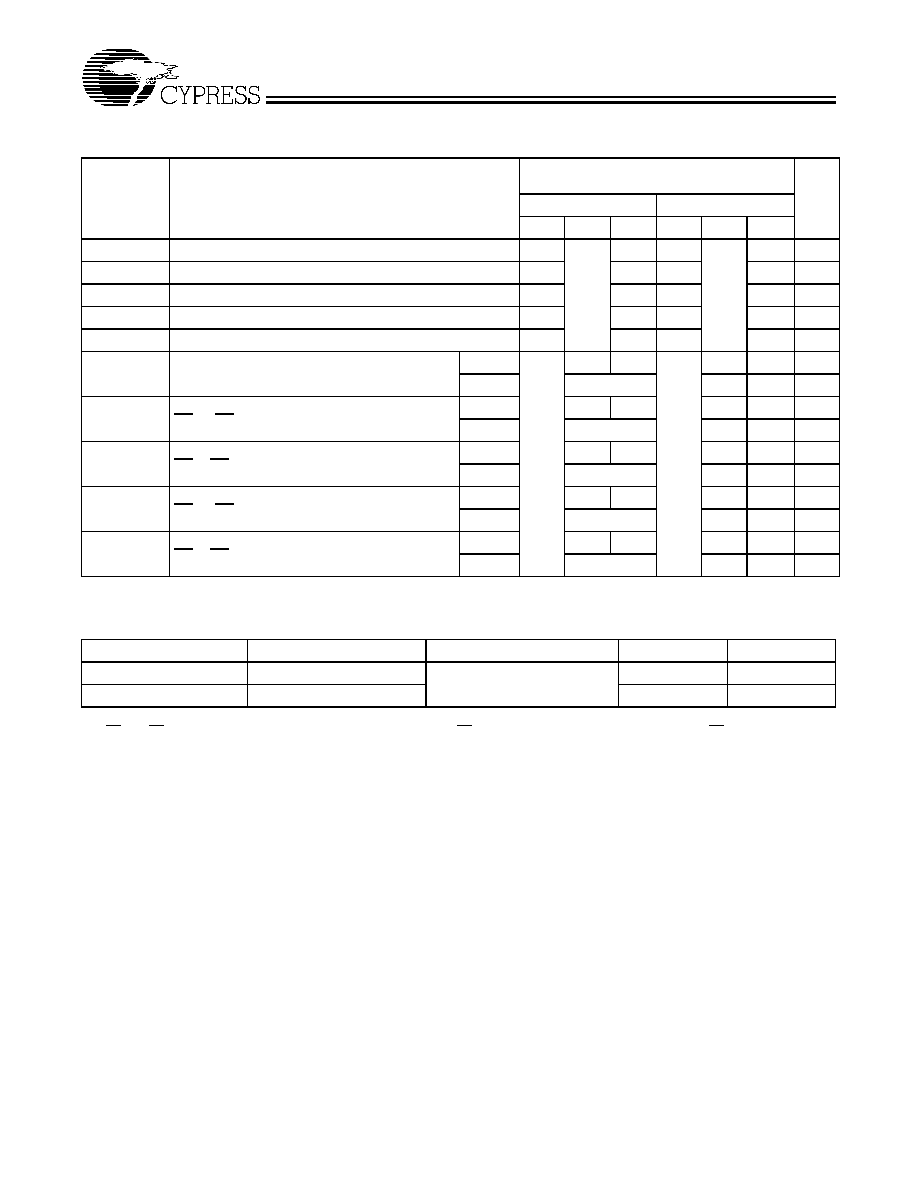
Electrical Characteristics
Over the Operating Range
Parameter
Description
CY7C09159AV
CY7C09169AV
Unit
-9
-12
Min.
Typ.
Max.
Min.
Typ.
Max.
V
OH
Output HIGH Voltage (V
CC
= Min., I
OH
= ≠4.0 mA)
2.4
2.4
V
V
OL
Output LOW Voltage (V
CC
= Min., I
OH
= +4.0 mA)
0.4
0.4
V
V
IH
Input HIGH Voltage
2.0
2.0
V
V
IL
Input LOW Voltage
0.8
0.8
V
I
OZ
Output Leakage Current
≠10
10
≠10
10
µ
A
I
CC
Operating Current (V
CC
= Max.,
I
OUT
= 0 mA) Outputs Disabled
Com'l.
135
230
115
180
mA
Ind.
[4]
155
250
mA
I
SB1
Standby Current (Both Ports TTL Level)
[5]
CE
L
& CE
R
V
IH
, f = f
MAX
Com'l.
20
75
20
70
mA
Ind.
[4]
30
80
mA
I
SB2
Standby Current (One Port TTL Level)
[5]
CE
L
| CE
R
V
IH
, f = f
MAX
Com'l.
95
155
85
140
mA
Ind.
[4]
95
150
mA
I
SB3
Standby Current (Both Ports CMOS Level)
[5]
CE
L
& CE
R
V
CC
≠ 0.2V, f = 0
Com'l.
10
500
10
500
µ
A
Ind.
[4]
10
500
µ
A
I
SB4
Standby Current (One Port CMOS Level)
[5]
CE
L
| CE
R
V
IH
, f = f
MAX
Com'l.
85
115
75
100
mA
Ind.
[4]
85
110
mA
Capacitance
Parameter
Description
Test Conditions
Max.
Unit
C
IN
Input Capacitance
T
A
= 25
∞
C, f = 1 MHz,
V
CC
= 3.3V
10
pF
C
OUT
Output Capacitance
10
pF