Äîêóìåíòàöèÿ è îïèñàíèÿ www.docs.chipfind.ru
1M x 4 Static RAM
CY7C1046CV33
Cypress Semiconductor Corporation
·
3901 North First Street
·
San Jose
·
CA 95134
·
408-943-2600
Document #: 38-05003 Rev. *A
Revised September 13, 2002
Features
· High speed
-- t
AA
= 10ns
· Low active power for 10 ns speed
-- 324 mW (max.)
· 2.0V data retention
· Automatic power-down when deselected
· TTL-compatible inputs and outputs
· Easy memory expansion with CE and OE features
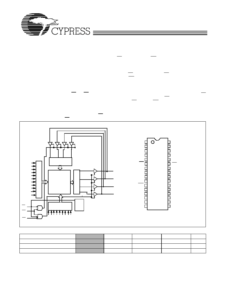
Functional Description
[1]
The CY7C1046CV33 is a high-performance CMOS static
RAM organized as 1,048,576 words by 4 bits. Easy memory
expansion is provided by an active LOW Chip Enable (CE), an
active LOW Output Enable (OE), and three-state drivers.
Writing to the device is accomplished by taking Chip Enable
(CE) and Write Enable (WE) inputs LOW. Data on the four I/O
pins (I/O
0
through I/O
3
) is then written into the location
specified on the address pins (A
0
through A
19
).
Reading from the device is accomplished by taking Chip
Enable (CE) and Output Enable (OE) LOW while forcing Write
Enable (WE) HIGH. Under these conditions, the contents of
the memory location specified by the address pins will appear
on the I/O pins.
The four input/output pins (I/O
0
through I/O
3
) are placed in a
high-impedance state when the device is deselected (CE
HIGH), the outputs are disabled (OE HIGH), or during a Write
operation (CE LOW, and WE LOW).
The CY7C1046CV33 is available in a standard 400-mil-wide
32-pin SOJ package with center power and ground (revolu-
tionary) pinout.
14
15
Logic Block Diagram
Pin Configuration
A
1
A
2
A
3
A
4
A
5
A
6
A
7
A
8
COLUMN
DECODER
ROW DEC
O
D
E
R
SE
NSE AM
PS
INPUT BUFFER
POWER
DOWN
WE
OE
I/O
0
I/O
1
1M x 4
ARRAY
I/O
3
I/O
2
A
0
A
11
A
13
A
12
A
CE
A
A
16
A
17
1
2
3
4
5
6
7
8
9
10
12
21
22
25
24
23
28
27
26
Top View
SOJ
11
29
32
31
30
14
13
19
20
GND
A
1
A
2
A
3
A
4
A
5
A
6
A
7
A
8
WE
V
CC
A
18
A
15
A
12
A
14
I/O
2
A
9
A
0
I/O
0
I/O
1
OE
A
17
A
16
A
13
CE
A
9
A
18
16
15
17
18
GND
I/O
3
V
CC
A
10
A
11
A
19
NC
A
10
A
19
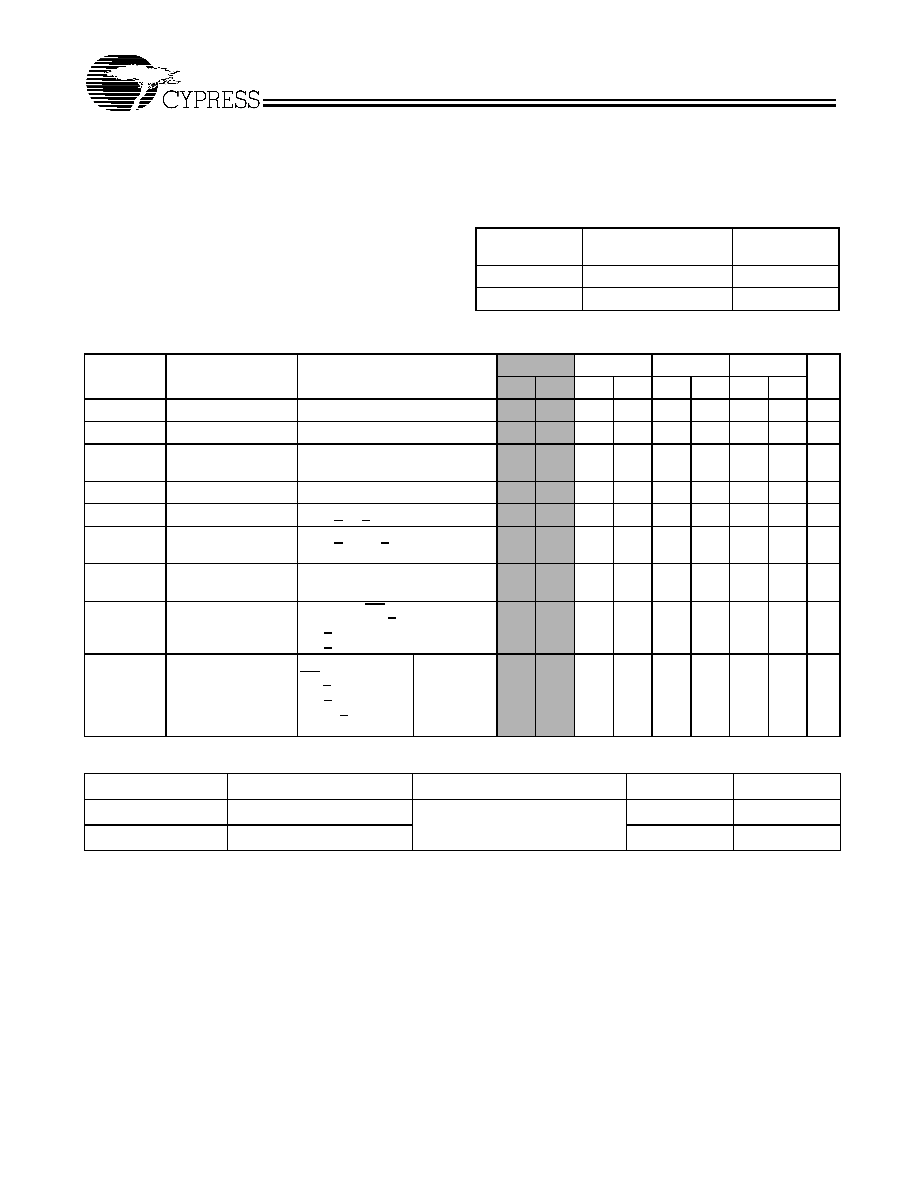
Selection Guide
-8
[2]
-10
-12
-15
Unit
Maximum Access Time
8
10
12
15
ns
Maximum Operating Current
100
90
85
80
mA
Maximum CMOS Standby Current
10
10
10
10
mA
Notes:
1.
For guidelines on SRAM system design, please refer to the `System Design Guidelines' Cypress application note, available on the internet at www.cypress.com.
2.
Shaded areas contain advance information.
CY7C1046CV33
Document #: 38-05003 Rev. *A
Page 2 of 9
Maximum Ratings
(Above which the useful life may be impaired. For user guide-
lines, not tested.)
Storage Temperature .................................65
°
C to +150
°
C
Ambient Temperature with
Power Applied............................................. 55
°
C to +125
°
C
Supply Voltage on V
CC
to Relative GND
[3]
.... 0.5V to +4.6V
DC Voltage Applied to Outputs
in High-Z State
[3]
....................................0.5V to V
CC
+ 0.5V
DC Input Voltage
[3]
.................................0.5V to V
CC
+ 0.5V
Current into Outputs (LOW)......................................... 20 mA
Static Discharge Voltage........................................... > 2001V
(per MIL-STD-883, Method 3015)
Latch-up Current..................................................... > 200 mA
Operating Range
Range
Ambient
Temperature
V
CC
Commercial
0
°
C to +70
°
C
3.0V 3.6V
Industrial
40
°
C to + 85
°
C
3.0V 3.6V
DC Electrical Characteristics
Over the Operating Range
Parameter
Description
Test Conditions
-8
[2]
-10
-12
-15
Unit
Min. Max. Min. Max. Min. Max. Min. Max.
V
OH
Output HIGH Voltage V
CC
= Min., I
OH
= 4.0 mA
2.4
2.4
2.4
2.4
V
V
OL
Output LOW Voltage V
CC
= Min., I
OL
= 8.0 mA
0.4
0.4
0.4
0.4
V
V
IH
Input HIGH Voltage
2.0
V
CC
+ 0.3
2.0
V
CC
+ 0.3
2.0
V
CC
+ 0.3
2.0
V
CC
+ 0.3
V
V
IL
Input LOW Voltage
[3]
0.3
0.8
0.3
0.8
0.3
0.8
0.3
0.8
V
I
IX
Input Load Current
GND < V
I
< V
CC
1
+1
1
+1
1
+1
1
+1
µ
A
I
OZ
Output Leakage
Current
GND < V
OUT
< V
CC
,
Output Disabled
1
+1
1
+1
1
+1
1
+1
µ
A
I
CC
V
CC
Operating
Supply Current
V
CC
= Max.,
f = f
MAX
= 1/t
RC
100
90
85
80
mA
I
SB1
Automatic CE
Power-Down Current
-- TTL Inputs
Max. V
CC
, CE > V
IH
V
IN
> V
IH
or
V
IN
< V
IL
, f = f
MAX
40
40
40
40
mA
I
SB2
Automatic CE
Power-Down Current
-- CMOS Inputs
Max. V
CC
,
CE > V
CC
0.3V,
V
IN
> V
CC
0.3V,
or V
IN
< 0.3V,
f = 0
Commercial
10
10
10
10
mA
Capacitance
[4]
Parameter
Description
Test Conditions
Max.
Unit
C
IN
Input Capacitance
T
A
= 25
°
C, f = 1 MHz, V
CC
= 3.3V
6
pF
C
OUT
I/O Capacitance
6
pF
Notes:
3.
V
IL
(min.) = 2.0V for pulse durations of less than 20 ns.
4.
Tested initially and after any design or process changes that may affect these parameters.
CY7C1046CV33
Document #: 38-05003 Rev. *A
Page 3 of 9
AC Test Loads and Waveforms
[5]
Notes:
5.
AC characteristics (except High-Z) for all 8-ns and 10-ns parts are tested using the load conditions shown in Figure (a). All other speeds are tested using the
Thevenin load shown in Figure (b). High-Z characteristics are tested for all speeds using the test load shown in Figure (d).
90%
10%
3.0V
GND
90%
10%
ALL INPUT PULSES
3.3V
OUTPUT
30 pF
* CAPACITIVE LOAD CONSISTS
OF ALL COMPONENTS OF THE
TEST ENVIRONMENT
(b)
R 317
R2
351
Rise Time: 1 V/ns
Fall Time: 1 V/ns
30 pF*
OUTPUT
Z=50
50
1.5V
(c)
(a)
3.3V
OUTPUT
5 pF
(d)
R 317
R2
351
8-, 10-ns devices:
12-, 15-ns devices:
High-Z characteristics:
CY7C1046CV33
Document #: 38-05003 Rev. *A
Page 4 of 9
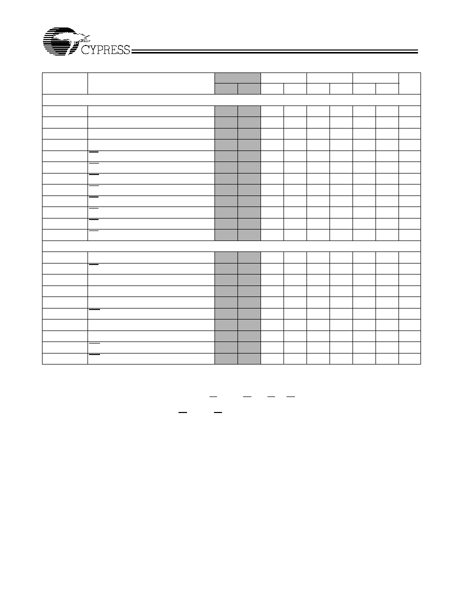
AC Switching Characteristics
[6]
Over the Operating Range
Parameter
Description
-8
[2]
-10
-12
-15
Unit
Min.
Max.
Min.
Max.
Min.
Max.
Min.
Max.
Read Cycle
t
power
[7]
V
CC
(typical) to the first access
1
1
1
1
µ
s
t
RC
Read Cycle Time
8
10
12
15
ns
t
AA
Address to Data Valid
8
10
12
15
ns
t
OHA
Data Hold from Address Change
3
3
3
3
ns
t
ACE
CE LOW to Data Valid
8
10
12
15
ns
t
DOE
OE LOW to Data Valid
4
5
6
7
ns
t
LZOE
OE LOW to Low-Z
[9]
0
0
0
0
ns
t
HZOE
OE HIGH to High-Z
[8, 9]
4
5
6
7
ns
t
LZCE
CE LOW to Low-Z
[9]
3
3
3
3
ns
t
HZCE
CE HIGH to High-Z
[8, 9]
4
5
6
7
ns
t
PU
CE LOW to Power-up
0
0
0
0
ns
t
PD
CE HIGH to Power-Down
8
10
12
15
ns
Write Cycle
[10, 11]
t
WC
Write Cycle Time
8
10
12
15
ns
t
SCE
CE LOW to Write End
6
7
8
10
ns
t
AW
Address Set-up to Write End
6
7
8
10
ns
t
HA
Address Hold from Write End
0
0
0
0
ns
t
SA
Address Set-up to Write Start
0
0
0
0
ns
t
PWE
WE Pulse Width
6
7
8
10
ns
t
SD
Data Set-up to Write End
4
5
6
7
ns
t
HD
Data Hold from Write End
0
0
0
0
ns
t
LZWE
WE HIGH to Low-Z
[9]
3
3
3
3
ns
t
HZWE
WE LOW to High-Z
[8, 9]
4
5
6
7
ns
Notes:
6.
Test conditions assume signal transition time of 3 ns or less, timing reference levels of 1.5V, input pulse levels of 0 to 3.0V.
7.
t
POWER
gives the minimum amount of time that the power supply should be at stable, typical Vcc values until the first memory access can be performed.
8.
t
HZOE
, t
HZCE
, and t
HZWE
are specified with a load capacitance of 5 pF as in part (d) of AC Test Loads. Transition is measured
±
500 mV from steady-state voltage.
9.
At any given temperature and voltage condition, t
HZCE
is less than t
LZCE
, t
HZOE
is less than t
LZOE
, and t
HZWE
is less than t
LZWE
for any given device.
10. The internal Write time of the memory is defined by the overlap of CE LOW, and WE LOW. CE and WE must be LOW to initiate a Write, and the transition of
either of these signals can terminate the Write. The input data set-up and hold timing should be referenced to the leading edge of the signal that terminates
the Write.
11.
The minimum Write cycle time for Write Cycle no. 3 (WE controlled, OE LOW) is the sum of t
HZWE
and t
SD
.
CY7C1046CV33
Document #: 38-05003 Rev. *A
Page 5 of 9
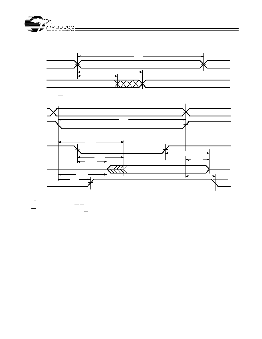
s
Switching Waveforms
Read Cycle No. 1
[14, 15]
Read Cycle No. 2 (OE Controlled)
[15, 16]
Notes:
12. t
r
< 3 ns for the -10, -12, and -15 speeds.
13. No input may exceed V
CC
+ 0.5V.
14. Device is continuously selected. OE, CE = V
IL
.
15. WE is HIGH for Read cycle.
16. Address valid prior to or coincident with CE transition LOW.
PREVIOUS DATA VALID
DATA VALID
t
RC
t
AA
t
OHA
ADDRESS
DATA OUT
50%
50%
DATA VALID
t
RC
t
ACE
t
DOE
t
LZOE
t
LZCE
t
PU
HIGH IMPEDANCE
t
HZOE
t
HZCE
t
PD
HIGH
OE
CE
I
CC
I
SB
IMPEDANCE
ADDRESS
DATA OUT
V
CC
SUPPLY
CURRENT