4-Mbit (512K x 8) Static RAM
CY7C1049CV33
Cypress Semiconductor Corporation
∑
3901 North First Street
∑
San Jose
,
CA 95134
∑
408-943-2600
Document #: 38-05006 Rev. *C
Revised July 19, 2004
Features
∑ Temperature Ranges
-- Commercial: 0∞C to 70∞C
-- Industrial: ≠40∞C to 85∞C
-- Automotive: ≠40∞C to 125∞C
∑ High speed
-- t
AA
= 10 ns
∑ Low active power
-- 324 mW (max.)
∑ 2.0V data retention
∑ Automatic power-down when deselected
∑ TTL-compatible inputs and outputs
∑ Easy memory expansion with CE and OE features
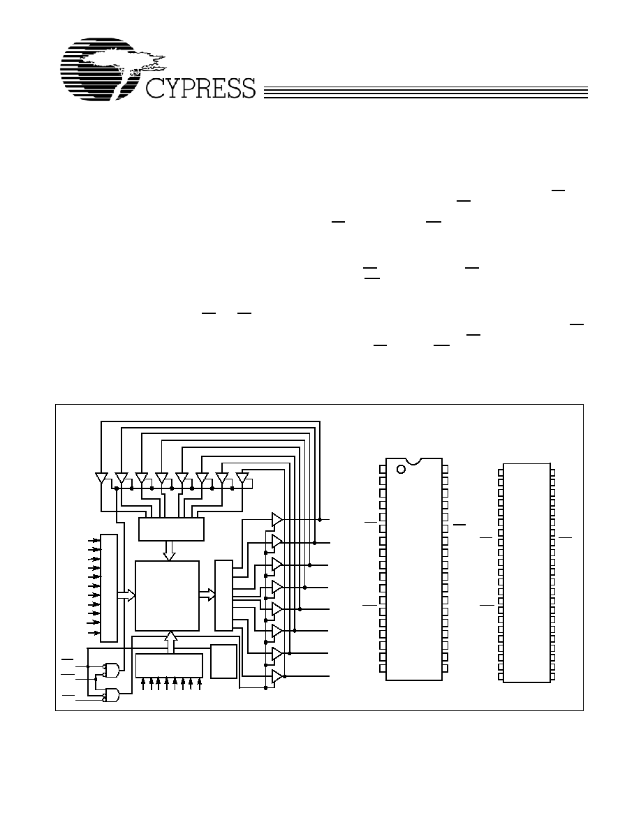
Functional Description
[1]
The CY7C1049CV33 is a high-performance CMOS Static
RAM organized as 524,288 words by 8 bits. Easy memory
expansion is provided by an active LOW Chip Enable (CE), an
active LOW Output Enable (OE), and three-state drivers.
Writing to the device is accomplished by taking Chip Enable
(CE) and Write Enable (WE) inputs LOW. Data on the eight I/O
pins (I/O
0
through I/O
7
) is then written into the location
specified on the address pins (A
0
through A
18
).
Reading from the device is accomplished by taking Chip
Enable (CE) and Output Enable (OE) LOW while forcing Write
Enable (WE) HIGH. Under these conditions, the contents of
the memory location specified by the address pins will appear
on the I/O pins.
The eight input/output pins (I/O
0
through I/O
7
) are placed in a
high-impedance state when the device is deselected (CE
HIGH), the outputs are disabled (OE HIGH), or during a Write
operation (CE LOW, and WE LOW).
The CY7C1049CV33 is available in standard 400-mil-wide
36-pin SOJ package and 44-pin TSOP II package with center
power and ground (revolutionary) pinout.
Notes:
1. For guidelines on SRAM system design, please refer to the `System Design Guidelines' Cypress application note, available on the internet at www.cypress.com.
14
15
Logic Block Diagram
Pin Configuration
A
1
A
2
A
3
A
4
A
5
A
6
A
7
A
8
COLUMN
DECODER
RO
W
DEC
O
D
E
R
SEN
S
E
AM
P
S
INPUT BUFFER
POWER
DOWN
WE
OE
I/O
0
I/O
1
I/O
2
I/O
3
512K x 8
ARRAY
I/O
7
I/O
6
I/O
5
I/O
4
A
0
A
11
A
13
A
12
A
CE
A A
16
A
17
1
2
3
4
5
6
7
8
9
10
11
14
23
24
28
27
26
25
29
32
31
30
Top View
SOJ
12
13
33
36
35
34
16
15
21
22
GND
A
1
A
2
A
3
A
4
A
5
A
6
A
7
A
8
WE
V
CC
A
18
A
15
A
12
A
14
I/O
5
I/O
4
A
9
A
0
I/O
0
I/O
1
I/O
2
OE
A
17
A
16
A
13
CE
A
9
A
18
18
17
19
20
GND
I/O
7
I/O
3
I/O
6
V
CC
A
10
A
11
NC
NC
A
10
A
6
1
2
3
4
5
6
7
8
9
10
11
14
31
32
36
35
34
33
37
40
39
38
Top View
TSOP II
12
13
41
44
43
42
16
15
29
30
V
CC
A
7
A
8
A
9
NC
NC
NC
NC
A
18
V
SS
NC
A
15
A
0
A
3
I/O
0
A
4
CE
A
17
A
12
A
1
A
2
18
17
20
19
I/O
1
27
28
25
26
22
21
23
24
NC
V
SS
WE
I/O
2
I/O
3
A
5
NC
A
16
V
CC
OE
I/O
7
I/O
6
I/O
5
I/O
4
A
14
A
13
A
11
A
10
NC
NC
NC
CY7C1049CV33
Document #: 38-05006 Rev. *C
Page 2 of 9
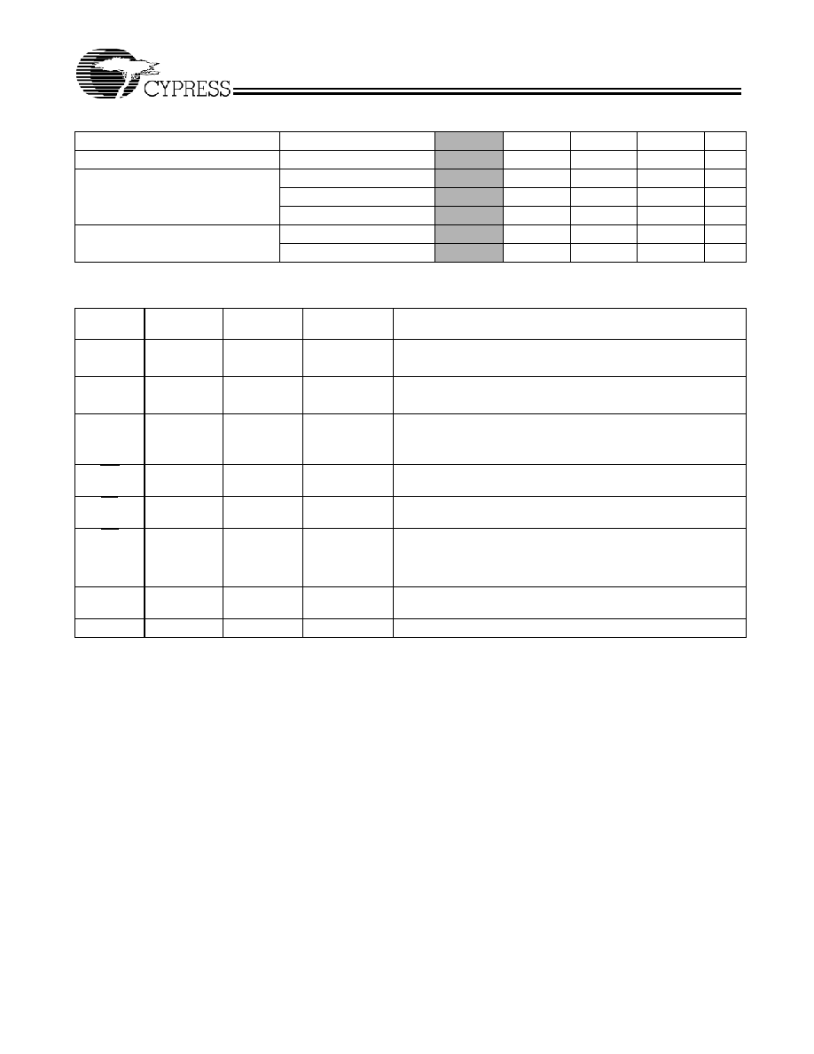
Selection Guide
-8
[]
-10
-12
-15
Unit
Maximum Access Time
8
10
12
15
ns
Maximum Operating Current
Commercial
100
90
85
80
mA
Industrial
110
100
95
90
mA
Automotive
-
-
-
95
mA
Maximum CMOS Standby Current
Commercial / Industrial
10
10
10
10
mA
Automotive
-
-
-
15
mA
Shaded areas contain advance information.
Pin Definitions
Pin Name
36-SOJ
Pin Number
44 TSOP-II
Pin Number
I/O Type
Description
A
0
-A
18
1-5,14-18,
20-24,32-35
3-7,16-20,
26-30,38-41
Input
Address Inputs used to select one of the address locations.
I/O
0
- I/O
7
7,8,11,12,25,
26,29,30
9,10,13,14,
31,32,35,36
Input/Output
Bidirectional Data I/O lines. Used as input or output lines
depending on operation
NC
[2]
19,36
1,2,21,22,23,
24,25,42,43,
44
No Connect
No Connects. This pin is not connected to the die
WE
13
15
Input/Control
Write Enable Input, active LOW. When selected LOW, a WRITE
is conducted. When selected HIGH, a READ is conducted.
CE
6
8
Input/Control
Chip Enable Input, active LOW. When LOW, selects the chip.
When HIGH, deselects the chip.
OE
31
37
Input/Control
Output Enable, active LOW. Controls the direction of the I/O pins.
When LOW, the I/O pins are allowed to behave as outputs. When
deasserted HIGH, I/O pins are three-stated, and act as input data
pins.
V
SS
, GND
10,28
12,34
Ground
Ground for the device. Should be connected to ground of the
system.
V
CC
9,27
11,33
Power Supply Power Supply inputs to the device.
Notes:
2. NC pins are not connected on the die.
CY7C1049CV33
Document #: 38-05006 Rev. *C
Page 3 of 9
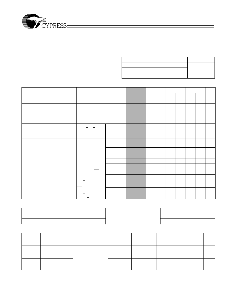
Maximum Ratings
(Above which the useful life may be impaired. For user guide-
lines, not tested.)
Storage Temperature .................................≠65
∞
C to +150
∞
C
Ambient Temperature with
Power Applied.............................................≠55
∞
C to +125
∞
C
Supply Voltage on V
CC
to Relative GND
[3]
.... ≠0.5V to +4.6V
DC Voltage Applied to Outputs
in High-Z State
[3]
.................................... ≠0.5V to V
CC
+ 0.5V
DC Input Voltage
[3]
................................ ≠0.5V to V
CC
+ 0.5V
Current into Outputs (LOW)......................................... 20 mA
Operating Range
Range
Ambient Temperature
V
CC
Commercial
0
∞
C to +70
∞
C
3.3V
±
0.3V
Industrial
≠40
∞
C to +85
∞
C
Automotive
≠40
∞
C to +125
∞
C
Electrical Characteristics
Over the Operating Range
Parame-
ter
Description
Test Conditions
-8
[]
-10
-12
-15
Unit
Min. Max. Min. Max. Min. Max. Min. Max.
V
OH
Output HIGH Voltage
V
CC
= Min.; I
OH
= ≠4.0 mA
2.4
2.4
2.4
2.4
V
V
OL
Output LOW Voltage
V
CC
= Min.,; I
OL
= 8.0 mA
0.4
0.4
0.4
0.4
V
V
IH
Input HIGH Voltage
2.0
V
CC
+ 0.3
2.0
V
CC
+ 0.3
2.0
V
CC
+ 0.3
2.0
V
CC
+ 0.3
V
V
IL
Input LOW Voltage
[3]
≠0.3
0.8
≠0.3
0.8
≠0.3
0.8
≠0.3
0.8
V
I
IX
Input Load Current
GND < V
I
< V
CC
Com'l / Ind'l
≠1
+1
≠1
+1
≠1
+1
≠1
+1
µ
A
Automotive
-
-
-
-
-
-
≠20
+20
µ
A
I
OZ
Output Leakage
Current
GND < V
OUT
<
V
CC
,
Output Disabled
Com'l / Ind'l
≠1
+1
≠1
+1
≠1
+1
≠1
+1
µ
A
Automotive
-
-
-
-
-
-
≠20
+20
µ
A
I
CC
V
CC
Operating
Supply Current
V
CC
= Max.,
f = f
MAX
= 1/t
RC
Com'l
100
90
85
80
mA
Ind'l
110
100
95
90
mA
Automotive
-
-
-
95
mA
I
SB1
Automatic CE
Power-down Current
--TTL Inputs
Max. V
CC
, CE >
V
IH
; V
IN
> V
IH
or
V
IN
< V
IL
, f = f
MAX
Com'l / Ind'l
40
40
40
40
mA
Automotive
-
-
-
45
mA
I
SB2
Automatic CE
Power-down Current
--CMOS Inputs
Max. V
CC
,
CE > V
CC
≠ 0.3V,
V
IN
> V
CC
≠ 0.3V,
or V
IN
< 0.3V, f = 0
Com'l/Ind'l
10
10
10
10
mA
Automotive
-
-
-
15
mA
Capacitance
[4]
Parameter
Description
Test Conditions
Max.
Unit
C
IN
Input Capacitance
T
A
= 25
∞
C, f = 1 MHz,
V
CC
= 3.3V
8
pF
C
OUT
I/O Capacitance
8
pF
Thermal Resistance
[4]
Parameter
Description
Test Conditions
36-pin SOJ
(Non
Pb-Free)
36-pin SOJ
( Pb-Free)
44-TSOP-II
(Non
Pb-Free)
44-TSOP-II
( Pb-Free)
Unit
JA
Thermal Resistance
(Junction to
Ambient)
Test conditions follow
standard test methods
and procedures for
measuring thermal
impedance, per EIA /
JESD51.
46.51
46.51
41.66
41.66
∞
C/W
JC
Thermal Resistance
(Junction to Case)
18.8
18.8
10.56
10.56
∞
C/W
Notes:
3. V
IL
(min.) = ≠2.0V and V
IH
(max) = V
CC
+ 0.5V for pulse durations of less than 20 ns.
4. Tested initially and after any design or process changes that may affect these parameters.
CY7C1049CV33
Document #: 38-05006 Rev. *C
Page 4 of 9
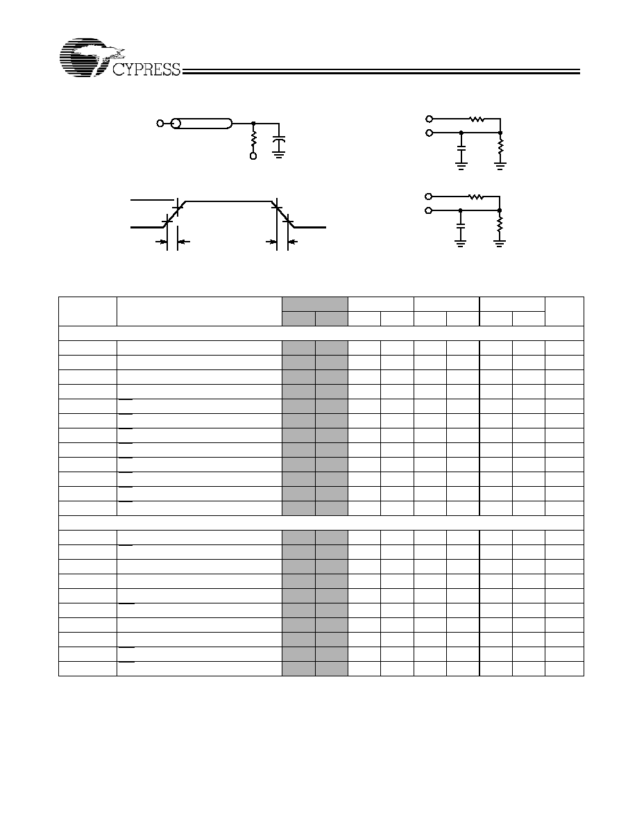
AC Test Loads and Waveforms
[5]
90%
10%
3.0V
GND
90%
10%
ALL INPUT PULSES
3.3V
OUTPUT
30 pF
* CAPACITIVE LOAD CONSISTS
OF ALL COMPONENTS OF THE
TEST ENVIRONMENT
(b)
R 317
R2
351
Rise Time: 1 V/ns
Fall Time: 1 V/ns
30 pF*
OUTPUT
Z = 50
50
1.5V
(c)
(a)
3.3V
OUTPUT
5 pF
(d)
R 317
R2
351
8-, 10-ns devices:
12-, 15-ns devices:
High-Z characteristics:
AC Switching Characteristics
[6]
Over the Operating Range
Parameter
Description
-8
[]
-10
-12
-15
Unit
Min.
Max.
Min.
Max.
Min.
Max.
Min.
Max.
Read Cycle
t
power
[7]
V
CC
(typical) to the first access
1
1
1
1
µ
s
t
RC
Read Cycle Time
8
10
12
15
ns
t
AA
Address to Data Valid
8
10
12
15
ns
t
OHA
Data Hold from Address Change
3
3
3
3
ns
t
ACE
CE LOW to Data Valid
8
10
12
15
ns
t
DOE
OE LOW to Data Valid
4
5
6
7
ns
t
LZOE
OE LOW to Low-Z
0
0
0
0
ns
t
HZOE
OE HIGH to High-Z
[8, 9]
4
5
6
7
ns
t
LZCE
CE LOW to Low-Z
[9]
3
3
3
3
ns
t
HZCE
CE HIGH to High-Z
[8, 9]
4
5
6
7
ns
t
PU
CE LOW to Power-up
0
0
0
0
ns
t
PD
CE HIGH to Power-down
8
10
12
15
ns
Write Cycle
[10, 11]
t
WC
Write Cycle Time
8
10
12
15
ns
t
SCE
CE LOW to Write End
6
7
8
10
ns
t
AW
Address Set-up to Write End
6
7
8
10
ns
t
HA
Address Hold from Write End
0
0
0
0
ns
t
SA
Address Set-up to Write Start
0
0
0
0
ns
t
PWE
WE Pulse Width
6
7
8
10
ns
t
SD
Data Set-up to Write End
4
5
6
7
ns
t
HD
Data Hold from Write End
0
0
0
0
ns
t
LZWE
WE HIGH to Low-Z
[9]
3
3
3
3
ns
t
HZWE
WE LOW to High-Z
[8, 9]
4
5
6
7
ns
Notes:
5. AC characteristics (except High-Z) for all 8-ns and 10-ns parts are tested using the load conditions shown in Figure (a). All other speeds are tested using the
Thevenin load shown in Figure (b). High-Z characteristics are tested for all speeds using the test load shown in Figure (d).
CY7C1049CV33
Document #: 38-05006 Rev. *C
Page 5 of 9
Switching Waveforms
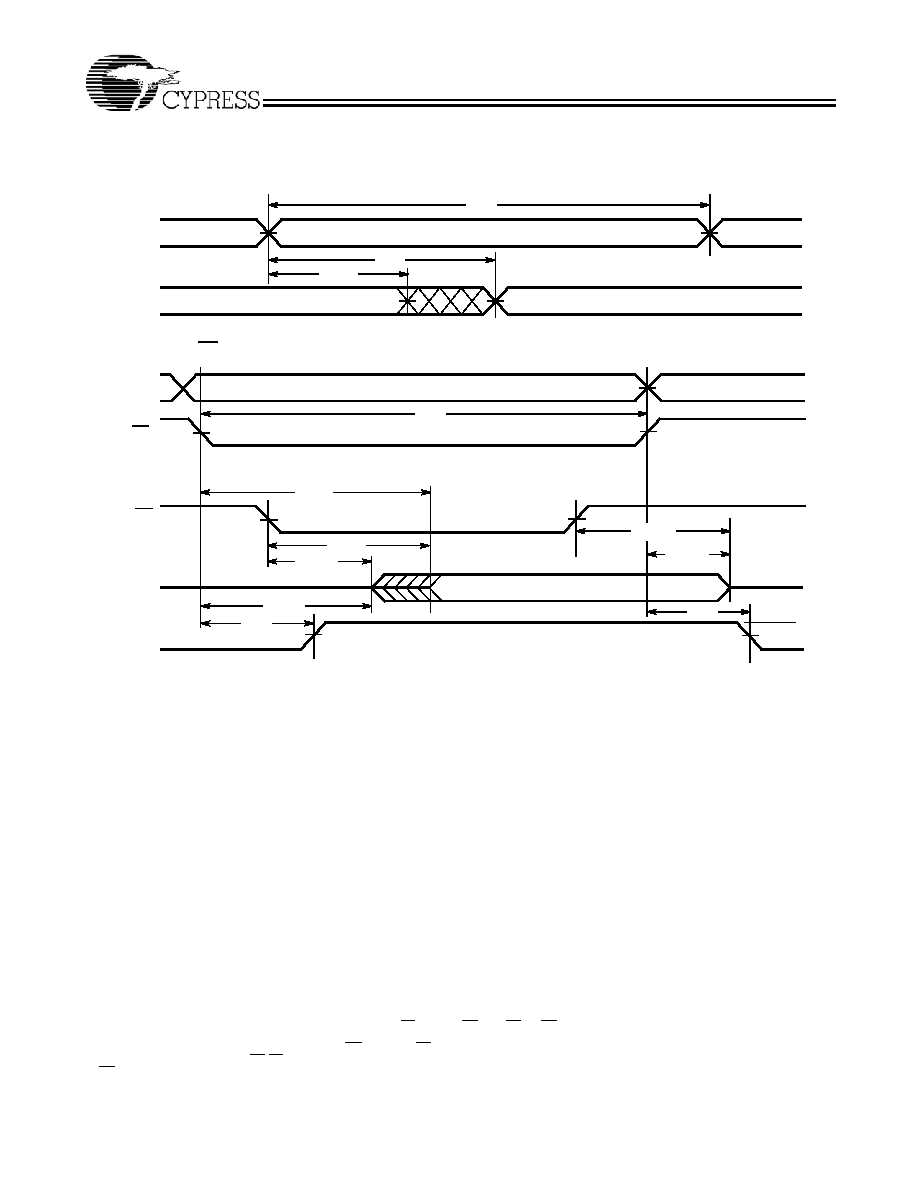
Read Cycle No. 1
[12, 13]
Read Cycle No. 2 (OE Controlled)
[13, 14]
Notes:
6. Test conditions assume signal transition time of 3 ns or less, timing reference levels of 1.5V, input pulse levels of 0 to 3.0V.
7. t
POWER
gives the minimum amount of time that the power supply should be at stable, typical V
CC
values until the first memory access can be performed.
8. t
HZOE
, t
HZCE
, and t
HZWE
are specified with a load capacitance of 5 pF as in part (d) of AC Test Loads. Transition is measured
±
500 mV from steady-state voltage.
9. At any given temperature and voltage condition, t
HZCE
is less than t
LZCE
, t
HZOE
is less than t
LZOE
, and t
HZWE
is less than t
LZWE
for any given device.
10. The internal Write time of the memory is defined by the overlap of CE LOW, and WE LOW. CE and WE must be LOW to initiate a Write, and the transition of either of these
signals can terminate the Write. The input data set-up and hold timing should be referenced to the leading edge of the signal that terminates the Write.
11. The minimum Write cycle time for Write Cycle No. 3 (WE controlled, OE LOW) is the sum of t
HZWE
and t
SD
.
12. Device is continuously selected. OE, CE = V
IL
.
13. WE is HIGH for Read cycle.
PREVIOUS DATA VALID
DATA VALID
t
RC
t
AA
t
OHA
ADDRESS
DATA OUT
50%
50%
DATA VALID
t
RC
t
ACE
t
DOE
t
LZOE
t
LZCE
t
PU
HIGH IMPEDANCE
t
HZOE
t
HZCE
t
PD
HIGH
OE
CE
I
CC
I
SB
IMPEDANCE
ADDRESS
DATA OUT
V
CC
SUPPLY
CURRENT