1M x 16 Static RAM
CY7C1061AV33
Cypress Semiconductor Corporation
∑
3901 North First Street
∑
San Jose
∑
CA 95134
∑
408-943-2600
Document #: 38-05256 Rev. *D
Revised February 21, 2003
Features
∑ High speed
-- t
AA
= 8, 10, 12 ns
∑ Low active power
-- 1080 mW (max.)
∑ Operating voltages of 3.3 ± 0.3V
∑ 2.0V data retention
∑ Automatic power-down when deselected
∑ TTL-compatible inputs and outputs
∑ Easy memory expansion with CE
1
and CE
2
features
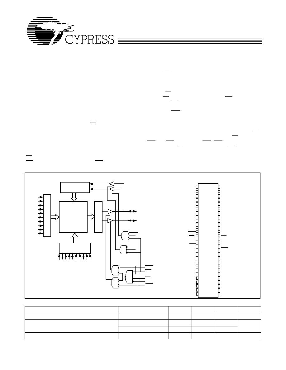
Functional Description
The CY7C1061AV33 is a high-performance CMOS Static
RAM organized as 1,048,576 words by 16 bits.
Writing to the device is accomplished by enabling the chip
(CE
1
LOW and CE
2
HIGH) while forcing the Write Enable
(WE) input LOW. If Byte Low Enable (BLE) is LOW, then data
from I/O pins (I/O
0
through I/O
7
), is written into the location
specified on the address pins (A
0
through A
19
). If Byte High
Enable (BHE) is LOW, then data from I/O pins (I/O
8
through
I/O
15
) is written into the location specified on the address pins
(A
0
through A
19
).
Reading from the device is accomplished by enabling the chip
by taking CE
1
LOW and CE
2
HIGH while forcing the Output
Enable (OE) LOW and the Write Enable (WE) HIGH. If Byte
Low Enable (BLE) is LOW, then data from the memory location
specified by the address pins will appear on I/O
0
to I/O
7
. If Byte
High Enable (BHE) is LOW, then data from memory will appear
on I/O
8
to I/O
15
. See the truth table at the back of this data
sheet for a complete description of Read and Write modes.
The input/output pins (I/O
0
through I/O
15
) are placed in a
high-impedance state when the device is deselected (CE
1
HIGH/CE
2
LOW), the outputs are disabled (OE HIGH), the
BHE and BLE are disabled (BHE, BLE HIGH), or during a
Write operation (CE
1
LOW, CE
2
HIGH, and WE LOW).
The CY7C1061AV33 is available in a 54-pin TSOP II package
with center power and ground (revolutionary) pinout, and a
48-ball fine-pitch ball grid array (FBGA) package.
Selection Guide
-8
-10
-12
Unit
Maximum Access Time
8
10
12
ns
Maximum Operating Current
Commercial
300
275
260
mA
Industrial
300
275
260
Maximum CMOS Standby Current
Commercial/Industrial
50
50
50
mA
Logic Block Diagram
Pin Configuration
TSOP II (Top View)
WE
1
2
3
4
5
6
7
8
9
10
11
14
31
32
36
35
34
33
37
40
39
38
12
13
41
43
42
16
15
29
30
A
5
A
6
A
7
A
8
A
0
A
1
OE
V
SS
A
17
I/O
15
A
2
CE
1
I/O
2
I/O
0
I/O
1
BHE
A
3
A
4
18
17
20
19
I/O
3
27
28
25
26
22
21
23
24
I/O
6
I/O
4
I/O
5
I/O
7
A
16
A
15
BLE
V
CC
I/O
14
I/O
13
I/O
12
I/O
10
I/O
9
I/O
8
A
14
A
13
A
12
A
11
A
9
A
10
CE
2
44
46
45
47
50
49
48
51
53
52
54
V
SS
V
CC
A
19
A
18
V
CC
V
CC
V
SS
DNU (Do Not Use)
V
SS
NC
V
CC
I/O
11
V
SS
15
16
A
1
A
2
A
3
A
4
A
5
A
6
A
7
A
8
COLUMN
DECODER
ROW DE
CODER
S
E
N
S
E AM
PS
INPUT BUFFER
1M x 16
ARRAY
A
0
A
12
A
14
A
13
A
A
A
17
A
18
A
10
A
11
4096 x 4096
I/O
0
≠I/O
7
OE
I/O
8
≠I/O
15
CE
1
WE
BLE
BHE
A
9
A
19
CE
2
CY7C1061AV33
Document #: 38-05256 Rev. *D
Page 2 of 11
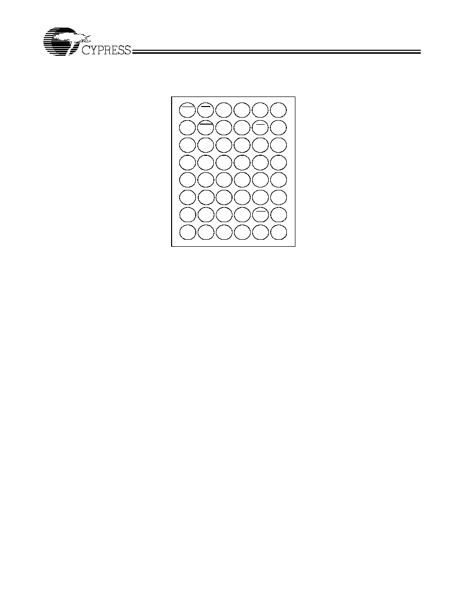
Pin Configurations
48-ball FBGA
WE
V
CC
A
11
A
10
NC
A
6
A
0
A
3
CE
1
I/O
10
I/O
8
I/O
9
A
4
A
5
I/O
11
I/O
13
I/O
12
I/O
14
I/O
15
V
SS
A
9
A
8
OE
V
SS
A
7
I/O
0
BHE
CE
2
A
17
A
2
A
1
BLE
V
CC
I/O
2
I/O
1
I/O
3
I/O
4
I/O
5
I/O
6
I/O
7
A
15
A
14
A
13
A
12
DNU
3
2
6
5
4
1
D
E
B
A
C
F
G
H
(Top View)
A
16
A
18
A
19
CY7C1061AV33
Document #: 38-05256 Rev. *D
Page 3 of 11
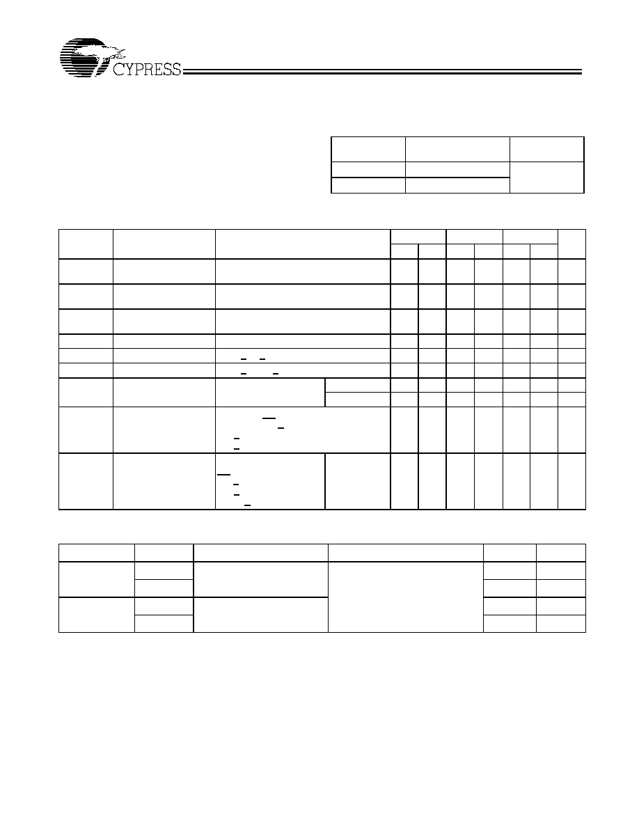
Maximum Ratings
(Above which the useful life may be impaired. For user guide-
lines, not tested.)
Storage Temperature .................................≠65
∞
C to +150
∞
C
Ambient Temperature with
Power Applied............................................. ≠55
∞
C to +125
∞
C
Supply Voltage on V
CC
to Relative GND
[1]
.... ≠0.5V to +4.6V
DC Voltage Applied to Outputs
in High-Z State
[1]
....................................≠0.5V to V
CC
+ 0.5V
DC Input Voltage
[1]
................................ ≠0.5V to V
CC
+ 0.5V
Current into Outputs (LOW)......................................... 20 mA
Operating Range
Range
Ambient
Temperature
V
CC
Commercial
0
∞
C to +70
∞
C
3.3V
±
0.3V
Industrial
≠40
∞
C to +85
∞
C
DC Electrical Characteristics
Over the Operating Range
Parameter
Description
Test Conditions
-8
-10
-12
Unit
Min. Max. Min. Max. Min. Max.
V
OH
Output HIGH Voltage
V
CC
= Min.,
I
OH
= ≠4.0 mA
2.4
2.4
2.4
V
V
OL
Output LOW Voltage
V
CC
= Min.,
I
OL
= 8.0 mA
0.4
0.4
0.4
V
V
IH
Input HIGH Voltage
2.0
V
CC
+ 0.3
2.0
V
CC
+ 0.3
2.0
V
CC
+ 0.3
V
V
IL
Input LOW Voltage
[1]
≠0.3
0.8
≠0.3
0.8
≠0.3
0.8
V
I
IX
Input Load Current
GND < V
I
< V
CC
≠1
+1
≠1
+1
≠1
+1
µ
A
I
OZ
Output Leakage Current GND < V
OUT
< V
CC
, Output Disabled
≠1
+1
≠1
+1
≠1
+1
µ
A
I
CC
V
CC
Operating
Supply Current
V
CC
= Max., f = f
MAX
=
1/t
RC
Commercial
300
275
260
mA
Industrial
300
275
260
mA
I
SB1
Automatic CE
Power-down Current
-- TTL Inputs
CE
2
<= V
IL
Max. V
CC
, CE > V
IH
V
IN
> V
IH
or
V
IN
< V
IL
, f = f
MAX
70
70
70
mA
I
SB2
Automatic CE
Power-down Current
-- CMOS Inputs
CE
2
<= 0.3V
Max. V
CC
,
CE > V
CC
≠ 0.3V,
V
IN
> V
CC
≠ 0.3V,
or V
IN
< 0.3V, f = 0
Commercial/
Industrial
50
50
50
mA
Capacitance
[2]
Parameter
Package
Description
Test Conditions
Max.
Unit
C
IN
Z54
Input Capacitance
T
A
= 25
∞
C, f = 1 MHz, V
CC
= 3.3V
6
pF
BA48
8
pF
C
OUT
Z54
I/O Capacitance
8
pF
BA48
10
pF
Notes:
1.
V
IL
(min.) = ≠2.0V for pulse durations of less than 20 ns.
2.
Tested initially and after any design or process changes that may affect these parameters.
CY7C1061AV33
Document #: 38-05256 Rev. *D
Page 4 of 11
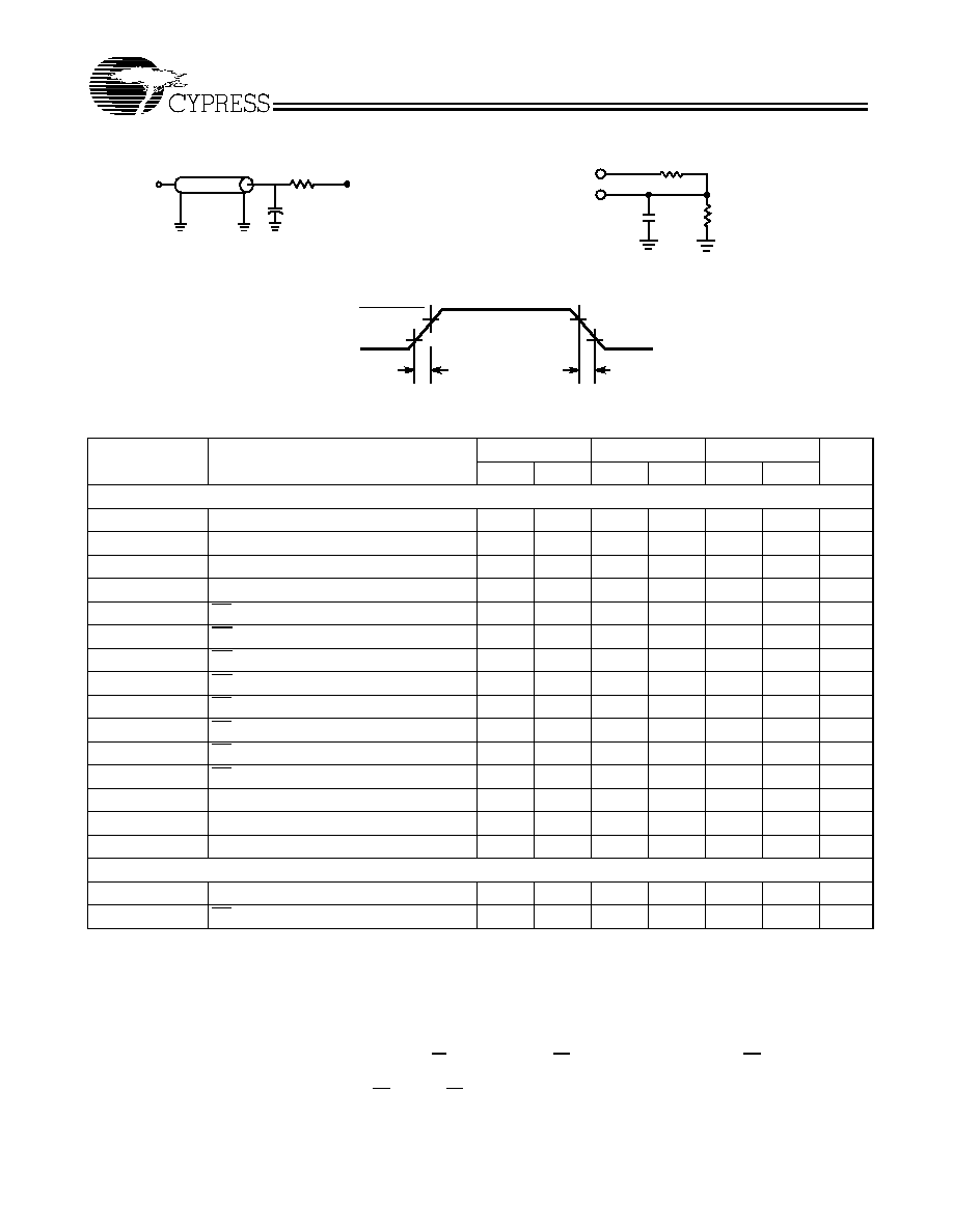
AC Test Loads and Waveforms
[3]
AC Switching Characteristics
Over the Operating Range
[4]
Parameter
Description
-8
-10
-12
Unit
Min.
Max.
Min.
Max.
Min.
Max.
Read Cycle
t
power
V
CC
(typical) to the first access
[5]
1
1
1
ms
t
RC
Read Cycle Time
8
10
12
ns
t
AA
Address to Data Valid
8
10
12
ns
t
OHA
Data Hold from Address Change
3
3
3
ns
t
ACE
CE
1
LOW / CE
2
HIGH to Data Valid
8
10
12
ns
t
DOE
OE LOW to Data Valid
5
5
6
ns
t
LZOE
OE LOW to Low-Z
1
1
1
ns
t
HZOE
OE HIGH to High-Z
[6]
5
5
6
ns
t
LZCE
CE
1
LOW/CE
2
HIGH to Low-Z
[6]
3
3
3
ns
t
HZCE
CE
1
HIGH/CE
2
LOW to High-Z
[6]
5
5
6
ns
t
PU
CE
1
LOW/CE
2
HIGH to Power-Up
[7]
0
0
0
ns
t
PD
CE
1
HIGH/CE
2
LOW to Power-Down
[7]
8
10
12
ns
t
DBE
Byte Enable to Data Valid
5
5
6
ns
t
LZBE
Byte Enable to Low-Z
1
1
1
ns
t
HZBE
Byte Disable to High-Z
5
5
6
ns
Write Cycle
[8, 9]
t
WC
Write Cycle Time
8
10
12
ns
t
SCE
CE
1
LOW/CE
2
HIGH to Write End
6
7
8
ns
Notes:
3.
Valid SRAM operation does not occur until the power supplies have reached the minimum operating V
DD
(3.0V). As soon as 1ms (T
power
) after reaching the
minimum operating V
DD
, normal SRAM operation can begin including reduction in V
DD
to the data retention (V
CCDR
, 2.0V) voltage.
4.
Test conditions assume signal transition time of 3 ns or less, timing reference levels of 1.5V, input pulse levels of 0 to 3.0V, and output loading of the specified
I
OL
/I
OH
and specified transmission line loads. Test conditions for the Read cycle use output loading shown in part a) of the AC test loads, unless specified otherwise.
5.
This part has a voltage regulator which steps down the voltage from 3V to 2V internally. t
power
time has to be provided initially before a Read/Write operation
is started.
6.
t
HZOE
, t
HZCE
, t
HZWE
, t
HZBE
and t
LZOE
, t
LZCE
, t
\LZWE
, t
LZBE
are specified with a load capacitance of 5 pF as in (b) of AC Test Loads. Transition is measured
±
200 mV from
steady-state voltage.
7.
These parameters are guaranteed by design and are not tested.
8.
The internal Write time of the memory is defined by the overlap of CE
1
LOW (CE
2
HIGH) and WE LOW. Chip enables must be active and WE and byte enables must
be LOW to initiate a Write, and the transition of any of these signals can terminate the Write. The input data set-up and hold timing should be referenced to the
leading edge of the signal that terminates the Write.
9.
The minimum Write cycle time for Write Cycle No. 3 (WE controlled, OE LOW) is the sum of t
HZWE
and t
SD
.
90%
10%
3.3V
GND
90%
10%
ALL INPUT PULSES
3.3V
OUTPUT
5 pF*
INCLUDING
JIG AND
SCOPE
(a)
(b)
R1 317
R2
351
Rise time > 1V/ns
Fall time:
> 1V/ns
(c)
OUTPUT
50
Z
0
= 50
V
TH
= 1.5V
30 pF*
* Capacitive Load consists of all com-
ponents of the test environment.
CY7C1061AV33
Document #: 38-05256 Rev. *D
Page 5 of 11
t
AW
Address Set-up to Write End
6
7
8
ns
t
HA
Address Hold from Write End
0
0
0
ns
t
SA
Address Set-up to Write Start
0
0
0
ns
t
PWE
WE Pulse Width
6
7
8
ns
t
SD
Data Set-up to Write End
5
5.5
6
ns
t
HD
Data Hold from Write End
0
0
0
ns
t
LZWE
WE HIGH to Low-Z
[6]
3
3
3
ns
t
HZWE
WE LOW to High-Z
[6]
5
5
6
ns
t
BW
Byte Enable to End of Write
6
7
8
ns
AC Switching Characteristics
Over the Operating Range (continued)
[4]
Parameter
Description
-8
-10
-12
Unit
Min.
Max.
Min.
Max.
Min.
Max.
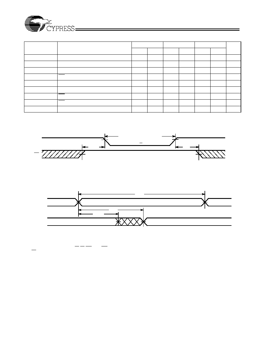
Data Retention Waveform
3.0V
3.0V
t
CDR
V
DR
> 2V
DATA RETENTION MODE
t
R
CE
V
CC
Switching Waveforms
Notes:
10. Device is continuously selected. OE, CE, BHE and/or BHE = V
IL
. CE2 = V
IH
.
11. WE is HIGH for Read cycle.
Read Cycle No. 1
PREVIOUS DATA VALID
DATA VALID
t
RC
t
AA
t
OHA
ADDRESS
DATA OUT
[10, 11]