PRELIMINARY
512K x 32 Static RAM
CY7C1062AV25
Cypress Semiconductor Corporation
∑
3901 North First Street
∑
San Jose
,
CA 95134
∑
408-943-2600
Document #: 38-05333 Rev. **
Revised January 27, 2003
Features
∑ High speed
-- t
AA
= 8, 10, 12 ns
∑ Low active power
-- 1080 mW (max.)
∑ Operating voltages of 2.5 ± 0.2V
∑ 1.5V data retention
∑ Automatic power-down when deselected
∑ TTL-compatible inputs and outputs
∑ Easy memory expansion with CE
1
, CE
2
, and CE
3
features
Functional Description
The CY7C1062AV25 is a high-performance CMOS Static
RAM organized as 524,288 words by 32 bits.
Writing to the device is accomplished by enabling the chip
(CE
1,
CE
2
and CE
3
LOW) and forcing the Write Enable (WE)
input LOW. If Byte Enable A (B
A
) is LOW, then data from I/O
pins (I/O
0
through I/O
7
), is written into the location specified on
the address pins (A
0
through A
18
). If Byte Enable B (B
B
) is
LOW, then data from I/O pins (I/O
8
through I/O
15
) is written
into the location specified on the address pins (A
0
through
A
18
). Likewise, B
C
and B
D
correspond with the I/O pins I/O
16
to I/O
23
and I/O
24
to I/O
31
, respectively.
Reading from the device is accomplished by enabling the chip
(CE
1,
CE
2
,
and CE
3
LOW) while forcing the Output Enable
(OE) LOW and Write Enable (WE) HIGH. If the first Byte
Enable (B
A
) is LOW, then data from the memory location
specified by the address pins will appear on I/O
0
to I/O
7
. If Byte
Enable B (B
B
) is LOW, then data from memory will appear on
I/O
8
to I/O
15
. Similarly, B
c
and B
D
correspond to the third and
fourth bytes. See the truth table at the back of this data sheet
for a complete description of read and write modes.
The input/output pins (I/O
0
through I/O
31
) are placed in a
high-impedance state when the device is deselected (CE
1,
CE
2
or CE
3
HIGH), the outputs are disabled (OE HIGH), the
byte selects are disabled (B
A-D
HIGH), or during a write
operation (CE
1,
CE
2
, and CE
3
LOW, and WE LOW).
The CY7C1062AV25 is available in a 119-ball pitch ball grid
array (PBGA) package.
Selection Guide
-8
-10
-12
Unit
Maximum Access Time
8
10
12
ns
Maximum Operating Current
Com'l
300
275
260
mA
Ind'l
300
275
260
Maximum CMOS Standby Current
Com'l/Ind'l
50
50
50
mA
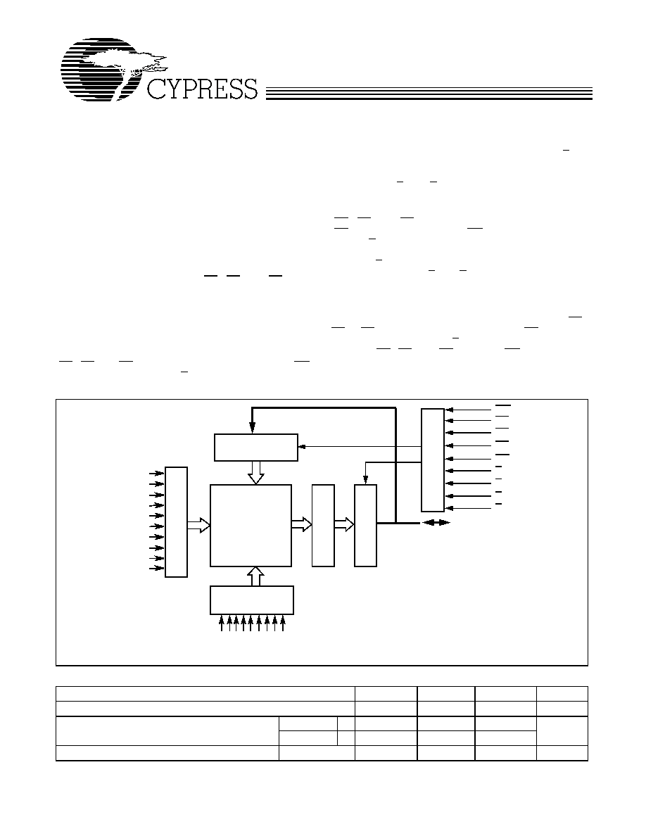
Logic Block Diagram
15
16
A 1
A 2
A 3
A 4
A 5
A 6
A 7
A 8
COLUMN
DECODER
RO
W D
E
CO
DE
R
S
E
N
S
E AM
P
S
INPUT BUFFERS
512K x 32
ARRAY
A 0
A
12
A
14
A
13
A
A A
17
A
18
A
10
A
11
4096 x 4096
I/O
0
≠I/O
31
OE
CE
3
B
A
B
D
A 9
O
U
TP
UT B
U
FFE
RS
CONT
R
O
L LOGI
C
B
B
B
C
WE
CE
2
CE
1
PRELIMINARY
CY7C1062AV25
Document #: 38-05333 Rev. **
Page 2 of 9
Pin Configuration
2
3
4
5
6
7
1
A
B
C
D
E
F
G
H
J
K
L
M
N
P
R
T
U
I/O
12
I/O
16
I/O
17
I/O
18
I/O
19
I/O
27
I/O
23
I/O
25
A
A
A
A
A
I/O
0
A
A
I/O
21
NC
I/O
26
I/O
31
I/O
29
I/O
30
B
c
V
SS
V
SS
V
DD
V
DD
A
V
SS
A
A
V
DD
CE
2
A
CE
1
A
A
I/O
1
NC
CE
3
B
a
I/O
2
V
SS
V
SS
V
SS
V
DD
I/O
4
I/O
6
V
SS
V
DD
V
DD
V
SS
I/O
8
A
A
A
I/O
15
OE
V
DD
V
SS
V
SS
V
DD
V
SS
V
SS
V
DD
V
SS
B
d
V
SS
V
DD
V
SS
V
SS
I/O
5
V
DD
V
SS
V
SS
V
SS
DNU
V
SS
V
DD
V
SS
V
SS
V
SS
V
SS
V
DD
V
SS
V
SS
I/O
10
V
DD
I/O
14
I/O
13
A
A
V
SS
V
SS
V
SS
NC
B
b
V
DD
I/O
3
WE
A
I/O
20
V
SS
V
DD
I/O
22
V
DD
V
SS
I/O
7
V
DD
I/O
9
I/O
11
V
DD
V
DD
I/O
24
V
SS
I/O
28
V
SS
V
DD
119-ball PBGA
V
DD
(Top View)
PRELIMINARY
CY7C1062AV25
Document #: 38-05333 Rev. **
Page 3 of 9
Maximum Ratings
(Above which the useful life may be impaired. For user guide-
lines, not tested.)
Storage Temperature .................................≠65
∞
C to +150
∞
C
Ambient Temperature with
Power Applied............................................. ≠55
∞
C to +125
∞
C
Supply Voltage on V
CC
to Relative GND
[1]
.... ≠0.5V to +3.6V
DC Voltage Applied to Outputs
in High-Z State
[1]
....................................≠0.5V to V
CC
+ 0.5V
DC Input Voltage
[1]
................................ ≠0.5V to V
CC
+ 0.5V
Current into Outputs (LOW)......................................... 20 mA
Operating Range
Range
Ambient
Temperature
V
CC
Commercial
0
∞
C to +70
∞
C
2.5V
±
0.2V
Industrial
≠40
∞
C to +85
∞
C
DC Electrical Characteristics
Over the Operating Range
Parameter
Description
Test Conditions
-8
-10
-12
Unit
Min.
Max.
Min.
Max.
Min.
Max.
V
OH
Output HIGH Voltage
V
CC
= Min.,
I
OH
= ≠1.0mA
2.0
2.0
2.0
V
V
OL
Output LOW Voltage
V
CC
= Min.,
I
OL
= 1.0 mA
0.4
0.4
0.4
V
V
IH
Input HIGH Voltage
2.0
V
CC
+ 0.3
2.0
V
CC
+ 0.3
2.0
V
CC
+ 0.3
V
V
IL
Input LOW Voltage
[1]
≠0.3
0.8
≠0.3
0.8
≠0.3
0.8
V
I
IX
Input Load Current
GND < V
I
< V
CC
≠1
+1
≠1
+1
≠1
+1
µ
A
I
OZ
Output Leakage Current
GND < V
OUT
< V
CC
, Output
Disabled
≠1
+1
≠1
+1
≠1
+1
µ
A
I
CC
V
CC
Operating
Supply Current
V
CC
= Max., f = f
MAX
= 1/t
RC
Com'l
300
275
260
mA
Ind'l
300
275
260
mA
I
SB1
Automatic CE
Power-down Current
--TTL Inputs
Max. V
CC
, CE > V
IH
V
IN
> V
IH
or
V
IN
< V
IL
, f = f
MAX
100
100
100
mA
I
SB2
Automatic CE
Power-down Current
--CMOS Inputs
Max. V
CC
,
CE > V
CC
≠ 0.2V,
V
IN
> V
CC
≠ 0.2V,
or V
IN
< 0.2V, f = 0
Com'l/Ind'l
50
50
50
mA
Capacitance
[2]
Parameter
Description
Test Conditions
Max.
Unit
C
IN
Input Capacitance
T
A
= 25
∞
C, f = 1 MHz, V
CC
= 2.5V
8
pF
C
OUT
I/O Capacitance
10
pF
Notes:
1.
V
IL
(min.) = ≠2.0V for pulse durations of less than 20 ns.
2.
Tested initially and after any design or process changes that may affect these parameters.
PRELIMINARY
CY7C1062AV25
Document #: 38-05333 Rev. **
Page 4 of 9
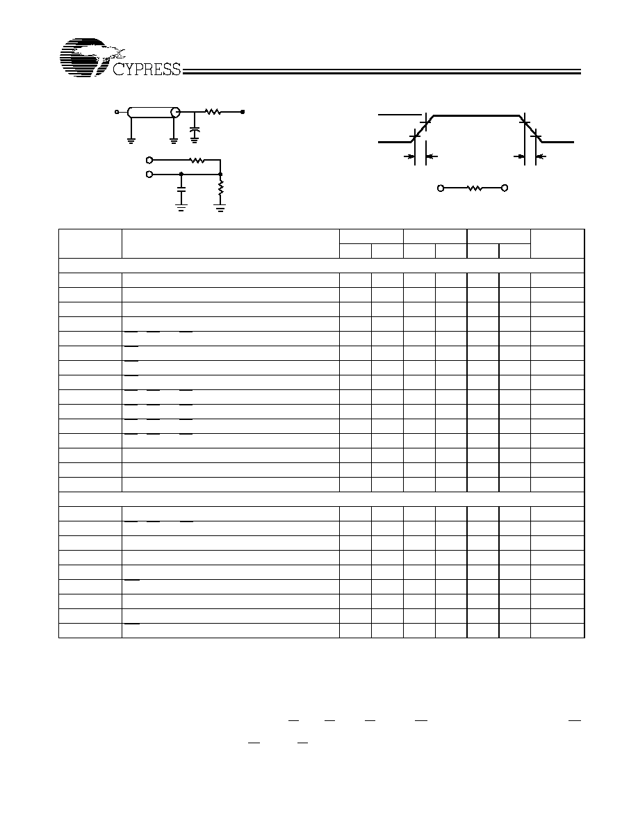
AC Test Loads and Waveforms
[3]
AC Switching Characteristics
Over the Operating Range
[4]
Parameter
Description
-8
-10
-12
Unit
Min.
Max.
Min.
Max.
Min.
Max.
Read Cycle
t
power
V
CC
(typical) to the first access
[5]
1
1
1
ms
t
RC
Read Cycle Time
8
10
12
ns
t
AA
Address to Data Valid
8
10
12
ns
t
OHA
Data Hold from Address Change
3
3
3
ns
t
ACE
CE
1
, CE
2
,
or CE
3
LOW to Data Valid
8
10
12
ns
t
DOE
OE LOW to Data Valid
5
5
6
ns
t
LZOE
OE LOW to Low-Z
[6]
1
1
1
ns
t
HZOE
OE HIGH to High-Z
[6]
5
5
6
ns
t
LZCE
CE
1
, CE
2
,
or CE
3
LOW to Low-Z
[6]
3
3
3
ns
t
HZCE
CE
1
, CE
2
,
or CE
3
HIGH to High-Z
[6]
5
5
6
ns
t
PU
CE
1
, CE
2
,
or CE
3
LOW to Power-up
[7]
0
0
0
ns
t
PD
CE
1
, CE
2
,
or CE
3
HIGH to Power-down
[7]
8
10
12
ns
t
DBE
Byte Enable to Data Valid
5
5
6
ns
t
LZBE
Byte Enable to Low-Z
[6]
1
1
1
ns
t
HZBE
Byte Disable to High-Z
[6]
5
5
6
ns
Write Cycle
[8, 9]
t
WC
Write Cycle Time
8
10
12
ns
t
SCE
CE
1
, CE
2
, or CE
3
LOW to Write End
6
7
8
ns
t
AW
Address Set-up to Write End
6
7
8
ns
t
HA
Address Hold from Write End
0
0
0
ns
t
SA
Address Set-up to Write Start
0
0
0
ns
t
PWE
WE Pulse Width
6
7
8
ns
t
SD
Data Set-up to Write End
5
5.5
6
ns
t
HD
Data Hold from Write End
0
0
0
ns
t
LZWE
WE HIGH to Low-Z
[6]
3
3
3
ns
Notes:
3.
Valid SRAM operation does not occur until the power supplies have reached the minimum operating V
DD
(2.3V). As soon as 1ms (T
power
) after reaching the
minimum operating V
DD
, normal SRAM operation can begin including reduction in V
DD
to the data retention (V
CCDR
, 1.5V) voltage.
4.
Test conditions assume signal transition time of 3 ns or less, timing reference levels of 1.1V, input pulse levels of 0 to 2.3V, and output loading of the specified
I
OL
/I
OH
and transmission line loads. Test conditions for the read cycle use output loading as shown in (a) of AC Test Loads, unless specified otherwise.
5.
This part has a voltage regulator that steps down the voltage from 2.3V to 2V internally. t
power
time has to be provided initially before a read/write operation is
started.
6.
t
HZOE
, t
HZCE
, t
HZWE
, t
HZBE
, and t
LZOE
, t
LZCE
, t
LZWE
, and t
LZBE
are specified with a load capacitance of 5 pF as in (b) of AC Test Loads. Transition is measured
± 200 mV from steady-state voltage.
7.
These parameters are guaranteed by design and are not tested.
8.
The internal write time of the memory is defined by the overlap of CE1 LOW, CE 2 HIGH, CE3 LOW, and WE LOW. The chip enables must be active and WE
must be LOW to initiate a write, and the transition of any of these signals can terminate the write. The input data set-up and hold timing should be referenced
to the leading edge of the signal that terminates the write.
9.
The minimum write cycle time for Write Cycle No. 3 (WE controlled, OE LOW) is the sum of t
HZWE
and t
SD
.
90%
10%
2.5V
GND
90%
10%
ALL INPUT PULSES
2.5V
OUTPUT
5 pF
Including
Jig and
Scope
OUTPUT
(a)
(b)
R1 317
167
R2
351
VENIN EQUIVALENT
TH…
1.73V
Rise time > 1 V/ns
Fall time:
> 1 V/ns
(c)
OUTPUT
50
Z
0
= 50
V
TH
= V
DD
/2
30 pF
Including all Components
of Test Equipment
PRELIMINARY
CY7C1062AV25
Document #: 38-05333 Rev. **
Page 5 of 9
t
HZWE
WE LOW to High-Z
[6]
5
5
6
ns
t
BW
Byte Enable to End of Write
6
7
8
ns
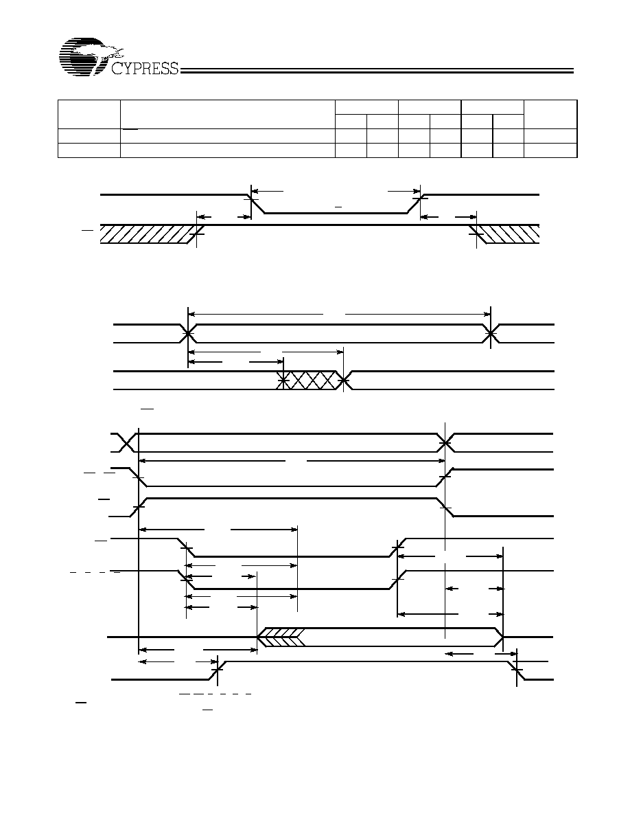
Data Retention Waveform
Switching Waveforms
Notes:
10. Device is continuously selected. OE, CE, B
A
, B
B
, B
C
, B
D
= V
IL
.
11. WE is HIGH for read cycle.
12. Address valid prior to or coincident with CE transition LOW.
AC Switching Characteristics
Over the Operating Range
[4]
(continued)
Parameter
Description
-8
-10
-12
Unit
Min.
Max.
Min.
Max.
Min.
Max.
2.3V
2.3V
t
CDR
V
DR
> 1.5V
DATA RETENTION MODE
t
R
CE
V
CC
Read Cycle No. 1
PREVIOUS DATA VALID
DATA VALID
t
RC
t
AA
t
OHA
ADDRESS
DATA OUT
[10, 11]
Read Cycle No. 2 (OE Controlled)
50%
50%
DATA VALID
t
RC
t
ACE
t
DOE
t
LZOE
t
LZCE
t
PU
HIGH IMPEDANCE
t
HZOE
t
HZBE
t
PD
HIGH
OE
CE
1
, CE
3
ICC
I
SB
IMPEDANCE
ADDRESS
DATA OUT
V
CC
SUPPLY
t
DBE
t
LZBE
t
HZCE
B
A
, B
B
, B
C
, B
D
[11, 12]
CURRENT
I
CC
CE
2