/home/web/doc/html/cypress/169448
1M x 1 Static RAM
CY7C107
CY7C1007
Cypress Semiconductor Corporation
·
3901 North First Street
·
San Jose
·
CA 95134
·
408-943-2600
Document #: 38-05034 Rev. **
Revised August 24, 2001
007
Features
· High speed
-- t
AA
= 12 ns
· CMOS for optimum speed/power
· Low active power
-- 825 mW
· Low standby power
-- 275 mW
· 2.0V data retention (optional)
-- 100
µ
W
· Automatic power-down when deselected
· TTL-compatible inputs and outputs
Functional Description
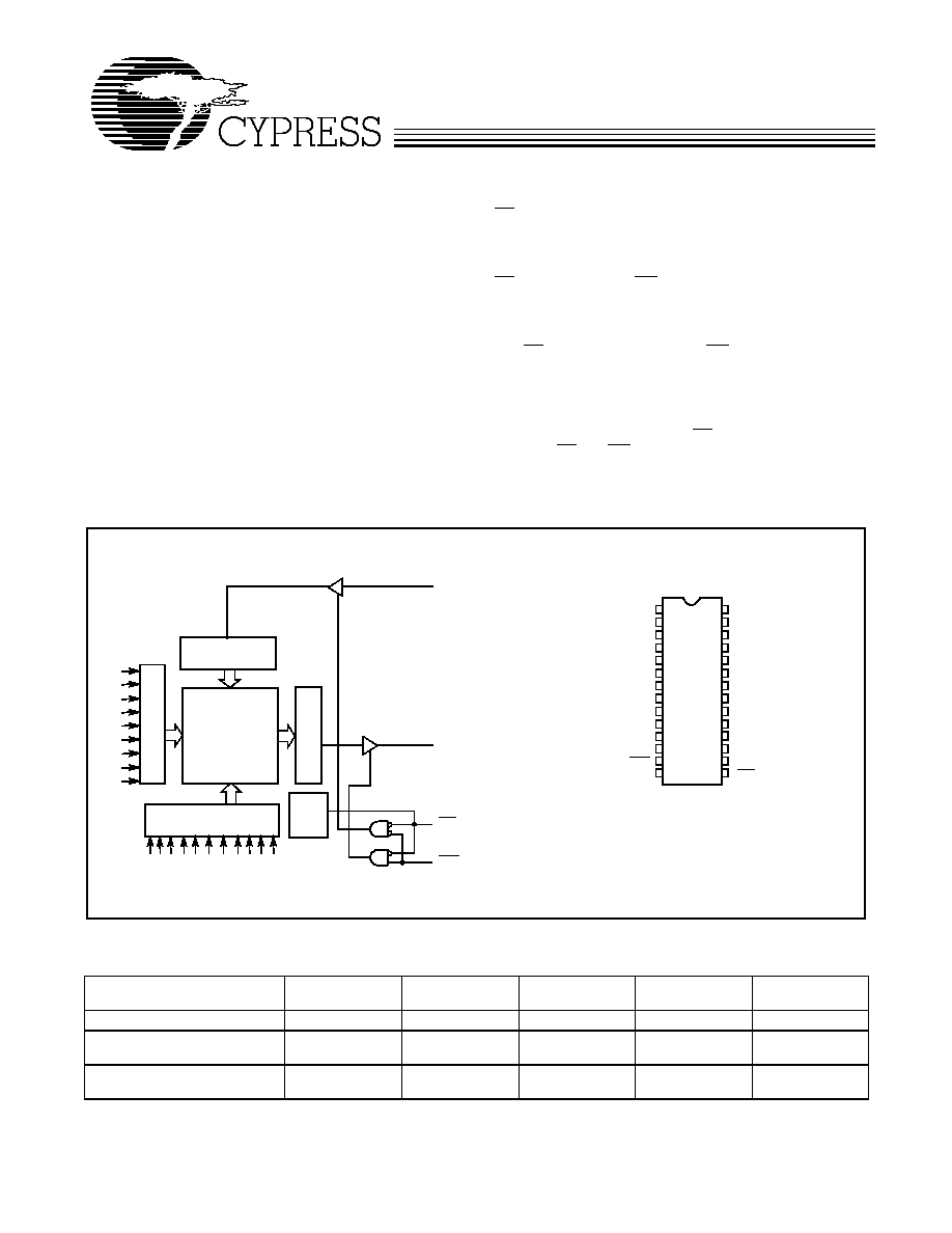
The CY7C107 and CY7C1007 are high-performance CMOS
static RAMs organized as 1,048,576 words by 1 bit. Easy
memory expansion is provided by an active LOW Chip Enable
(CE) and three-state drivers. These devices have an automat-
ic power-down feature that reduces power consumption by
more than 65% when deselected.
Writing to the devices is accomplished by taking Chip Enable
(CE) and Write Enable (WE) inputs LOW. Data on the input pin
(D
IN
) is written into the memory location specified on the ad-
dress pins (A
0
through A
19
).
Reading from the devices is accomplished by taking Chip En-
able (CE) LOW while Write Enable (WE) remains HIGH. Under
these conditions, the contents of the memory location speci-
fied by the address pins will appear on the data output (D
OUT
)
pin.
The output pin (D
OUT
) is placed in a high-impedance state
when the device is deselected (CE HIGH) or during a write
operation (CE and WE LOW).
The CY7C107 is available in a standard 400-mil-wide SOJ; the
CY7C1007 is available in a standard 300-mil-wide SOJ.
Logic Block Diagram
Pin Configuration
Top View
SOJ
512x2048
ARRAY
A
5
A
6
A
7
COLUMN
DECODER
ROW
DE
CODE
R
S
E
N
S
E AMP
S
POWER
DOWN
WE
CE
INPUT BUFFER
D
OUT
D
IN
A
4
A
3
A
2
A
1
A
0
1
2
3
4
5
6
7
8
9
10
11
14
15
16
20
19
18
17
21
24
23
22
12
13
25
28
27
26
GND
A
11
A
12
A
13
A
14
WE
V
CC
A
9
A
10
CE
A
0
D
OUT
D
IN
A
8
A
7
A
6
A
2
A
1
A
4
NC
NC
A
15
A
16
A
8
A
12
A
14
A
16
A
15
A
10
A
11
A
13
A
17
A
18
A
19
A
17
A
18
A
19
A
5
A
3
A
9
107-1
107-2
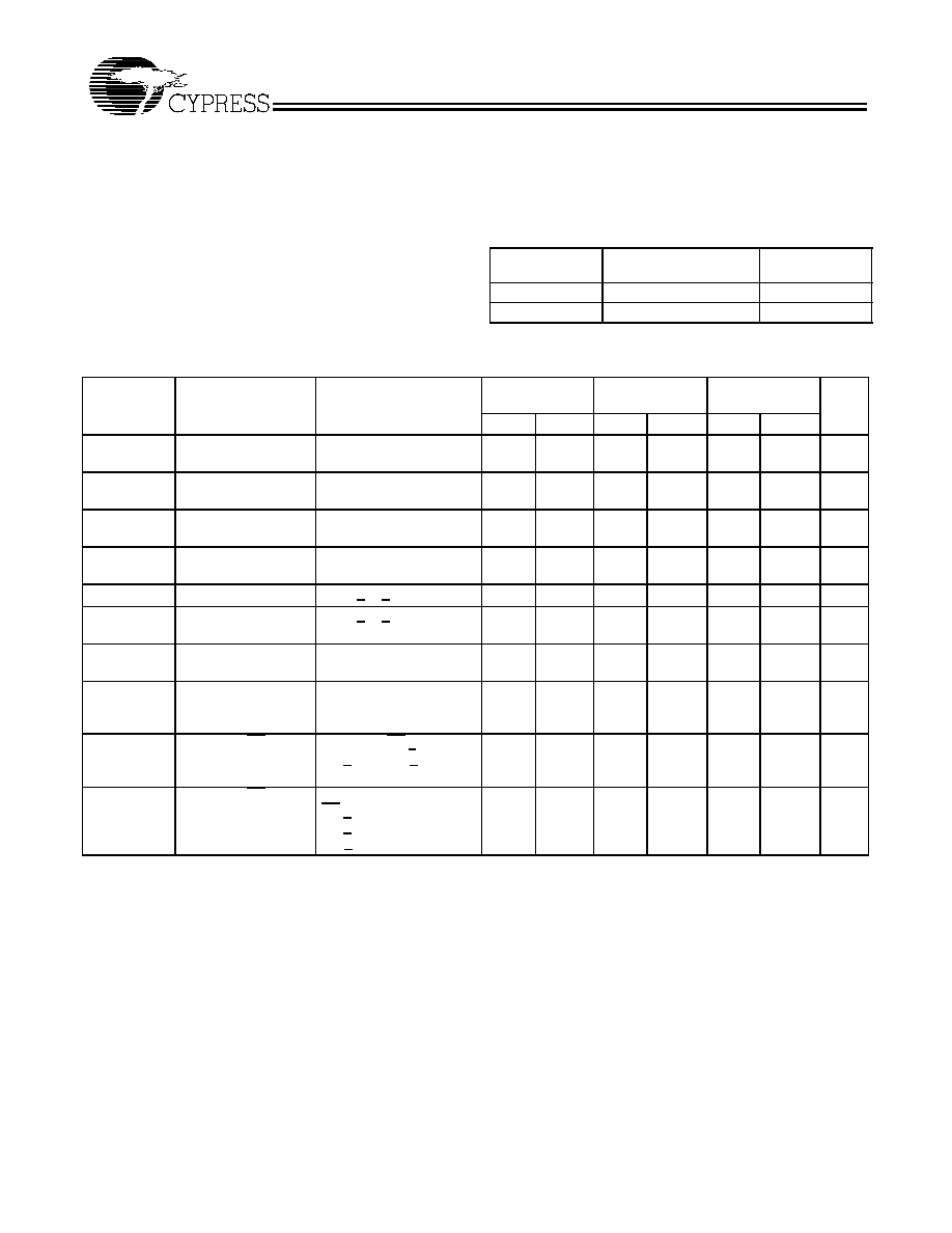
Selection Guide
7C107-12
7C1007-12
7C107-15
7C1007-15
7C107-20
7C1007-20
7C107-25
7C1007-25
7C107-35
Maximum Access Time (ns)
12
15
20
25
35
Maximum Operating
Current (mA)
150
135
125
120
110
Maximum Standby
Current (mA)
50
40
30
30
25
CY7C107
CY7C1007
Document #: 38-05034 Rev. **
Page 2 of 9
Maximum Ratings
(Above which the useful life may be impaired. For user guide-
lines, not tested.)
Storage Temperature
..................................... -
65°C to +150°C
Ambient Temperature with
Power Applied
.................................................. -
55°C to +125°C
Supply Voltage on V
CC
Relative to GND
[1]
.....-
0.5V to +7.0V
DC Voltage Applied to Outputs
in High Z State
[1]
....................................... -
0.5V to V
CC
+ 0.5V
DC Input Voltage
[1]
.................................... -
0.5V to V
CC
+ 0.5V
Current into Outputs (LOW) ........................................ 20 mA
Static Discharge Voltage ........................................... >2001V
(per MIL-STD-883, Method 3015)
Latch-Up Current ..................................................... >200 mA
Notes:
1.
V
IL
(min.) = 2.0V for pulse durations of less than 20 ns.
2.
T
A
is the "instant on" case temperature.
3.
Not more than 1 output should be shorted at one time. Duration of the short circuit should not exceed 30 seconds.
Operating Range
Range
Ambient
Temperature
[2]
V
CC
Commercial
0°C to +70°C
5V
±
10%
Industrial
-
40°C to +85°C
5V
±
10%
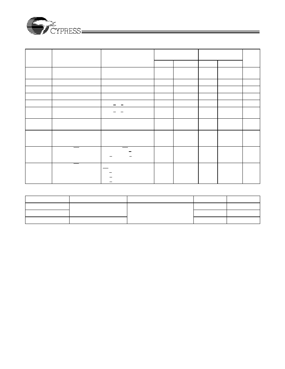
Electrical Characteristics
Over the Operating Range
Parameter
Description
Test Conditions
7C107-12
7C1007-12
7C107-15
7C1007-15
7C107-20
7C1007-20
Min.
Max.
Min.
Max.
Min.
Max.
Unit
V
OH
Output HIGH
Voltage
V
CC
= Min., I
OH
=
-
4.0 mA
2.4
2.4
2.4
V
V
OL
Output LOW
Voltage
V
CC
= Min., I
OL
= 8.0 mA
0.4
0.4
0.4
V
V
IH
Input HIGH
Voltage
2.2
V
CC
+
0.3
2.2
V
CC
+
0.3
2.2
V
CC
+
0.3
V
V
IL
Input LOW
Voltage
[1]
-
0.3
0.8
-
0.3
0.8
-
0.3
0.8
V
I
IX
Input Load Current
GND < V
I
< V
CC
-
1
+1
-
1
+1
-
1
+1
µ
A
I
OZ
Output Leakage
Current
GND < V
I
< V
CC
,
Output Disabled
5
+5
5
+5
5
+5
µ
A
I
OS
Output Short
Circuit Current
[3]
V
CC
= Max., V
OUT
= GND
-
300
-
300
-
300
mA
I
CC
V
CC
Operating
Supply Current
V
CC
= Max.,
I
OUT
= 0 mA,
f = f
MAX
= 1/t
RC
150
135
125
mA
I
SB1
Automatic CE
Power-Down
Current-- TTL Inputs
Max. V
CC
, CE > V
IH
,
V
IN
>V
IH
or V
IN
< V
IL
,
f = f
MAX
50
40
30
mA
I
SB2
Automatic CE
Power-Down
Current--
CMOS Inputs
Max. V
CC
,
CE > V
CC
0.3V,
V
IN
> V
CC
0.3V or
V
IN
< 0.3V, f = 0
2
2
2
mA
CY7C107
CY7C1007
Document #: 38-05034 Rev. **
Page 3 of 9
Electrical Characteristics
Over the Operating Range (continued)
Parameter
Description
Test Conditions
7C107-25
7C1007-25
7C107-35
Min.
Max.
Min.
Max.
Unit
V
OH
Output HIGH
Voltage
V
CC
= Min., I
OH
=
-
4.0 mA
2.4
2.4
V
V
OL
Output LOW Voltage
V
CC
= Min., I
OL
= 8.0 mA
0.4
0.4
V
V
IH
Input HIGH Voltage
2.2
V
CC
+ 0.3
2.2
V
CC
+ 0.3
V
V
IL
Input LOW Voltage
[1]
-
0.3
0.8
-
0.3
0.8
V
I
IX
Input Load Current
GND < V
I
< V
CC
-
1
+1
-
1
+1
µ
A
I
OZ
Output Leakage
Current
GND < V
I
< V
CC
,
Output Disabled
-
5
+5
-
5
+5
µ
A
I
OS
Output Short
Circuit Current
[3]
V
CC
= Max., V
OUT
= GND
-
300
-
300
mA
I
CC
V
CC
Operating
Supply Current
V
CC
= Max.,
I
OUT
= 0 mA,
f = f
MAX
= 1/t
RC
120
110
mA
I
SB1
Automatic CE
Power-Down
Current--TTL Inputs
Max. V
CC
, CE > V
IH
,
V
IN
>V
IH
or V
IN
< V
IL
,
f = f
MAX
30
25
mA
I
SB2
Automatic CE
Power-Down
Current--CMOS Inputs
Max. V
CC
,
CE > V
CC
0.3V,
V
IN
> V
CC
0.3V or
V
IN
< 0.3V, f = 0
2
2
mA
Capacitance
[4]
Parameter
Description
Test Conditions
Max.
Unit
C
IN
: Addresses
Input Capacitance
T
A
= 25
°
C, f = 1 MHz,
V
CC
= 5.0V
7
pF
C
IN
: Controls
10
pF
C
OUT
Output Capacitance
10
pF
Note:
4.
Tested initially and after any design or process changes that may affect these parameters.
CY7C107
CY7C1007
Document #: 38-05034 Rev. **
Page 4 of 9
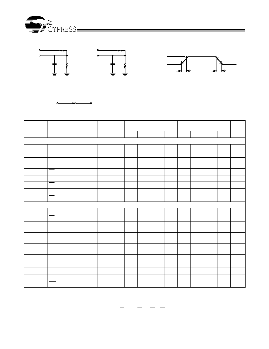
AC Test Loads and Waveforms
3.0V
5V
OUTPUT
R1 480
R2
255
30 pF
INCLUDING
JIG AND
SCOPE
GND
90%
10%
90%
10%
3 ns
3 ns
5V
OUTPUT
5 pF
INCLUDING
JIG AND
SCOPE
(a)
(b)
OUTPUT
1.73V
Equivalent to:
THÉ VENIN EQUIVALENT
ALL INPUT PULSES
R2
255
R1 480
167
107-3
107-4
Switching Characteristics
[5]
Over the Operating Range
7C107-12
7C1007-12
7C107-15
7C1007-15
7C107-20
7C1007-20
7C107-25
7C1007-25
7C107-35
Parameter
Description
Min.
Max.
Min.
Max.
Min.
Max.
Min.
Max.
Min.
Max.
Unit
READ CYCLE
t
RC
Read Cycle Time
12
15
20
25
35
ns
t
AA
Address to Data Valid
12
15
20
25
35
ns
t
OHA
Data Hold from Address
Change
3
3
3
3
3
ns
t
ACE
CE LOW to Data Valid
12
15
20
25
35
ns
t
LZCE
CE LOW to Low Z
[6]
3
3
3
3
3
ns
t
HZCE
CE HIGH to High Z
[6, 7]
6
7
8
10
10
ns
t
PU
CE LOW to Power-Up
0
0
0
0
0
ns
t
PD
CE HIGH to Power-Down
12
15
20
25
35
ns
WRITE CYCLE
[8]
t
WC
Write Cycle Time
12
15
20
25
35
ns
t
SCE
CE LOW to Write End
10
12
15
20
25
ns
t
AW
Address Set-Up to Write
End
10
12
15
20
25
ns
t
HA
Address Hold from Write
End
0
0
0
0
0
ns
t
SA
Address Set-Up to Write
Start
0
0
0
0
0
ns
t
PWE
WE Pulse Width
10
12
15
20
25
ns
t
SD
Data Set-Up to Write End
7
8
10
15
20
ns
t
HD
Data Hold from Write End
0
0
0
0
0
ns
t
LZWE
WE HIGH to Low Z
[6]
3
3
3
3
3
ns
t
HZWE
WE LOW to High Z
[6, 7]
6
7
8
10
10
ns
Notes:
5.
Test conditions assume signal transition time of 3 ns or less, timing reference levels of 1.5V, input pulse levels of 0 to 3.0V, and output loading of the specified
I
OL
/I
OH
and 30-pF load capacitance.
6.
At any given temperature and voltage condition, t
HZCE
is less than t
LZCE
and t
HZWE
is less than t
LZWE
for any given device.
7.
t
HZCE
and t
HZWE
are specified with a load capacitance of 5 pF as in part (b) of AC Test Loads. Transition is measured
±
500 mV from steady-state voltage.
8.
The internal write time of the memory is defined by the overlap of CE LOW and WE LOW. CE and WE must be LOW to initiate a write, and the transition of any of these
signals can terminate the write. The input data set-up and hold timing should be referenced to the leading edge of the signal that terminates the write.
CY7C107
CY7C1007
Document #: 38-05034 Rev. **
Page 5 of 9
Data Retention Characteristics
Over the Operating Range (L Version Only)
Parameter
Description
Conditions
[9]
Min.
Max.
Unit
V
DR
V
CC
for Data Retention
2.0
V
I
CCDR
Data Retention Current
V
CC
= V
DR
= 2.0V,
CE > V
CC
0.3V,
V
IN
> V
CC
0.3 or
V
IN
< 0.3V
50
µ
A
t
CDR
[4]
Chip Deselect to Data Retention Time
0
ns
t
R
[4]
Operation Recovery Time
t
RC
ns
Data Retention Waveform
4.5V
4.5V
CE
V
CC
t
CDR
V
DR
> 2V
DATA RETENTION MODE
t
R
107-5
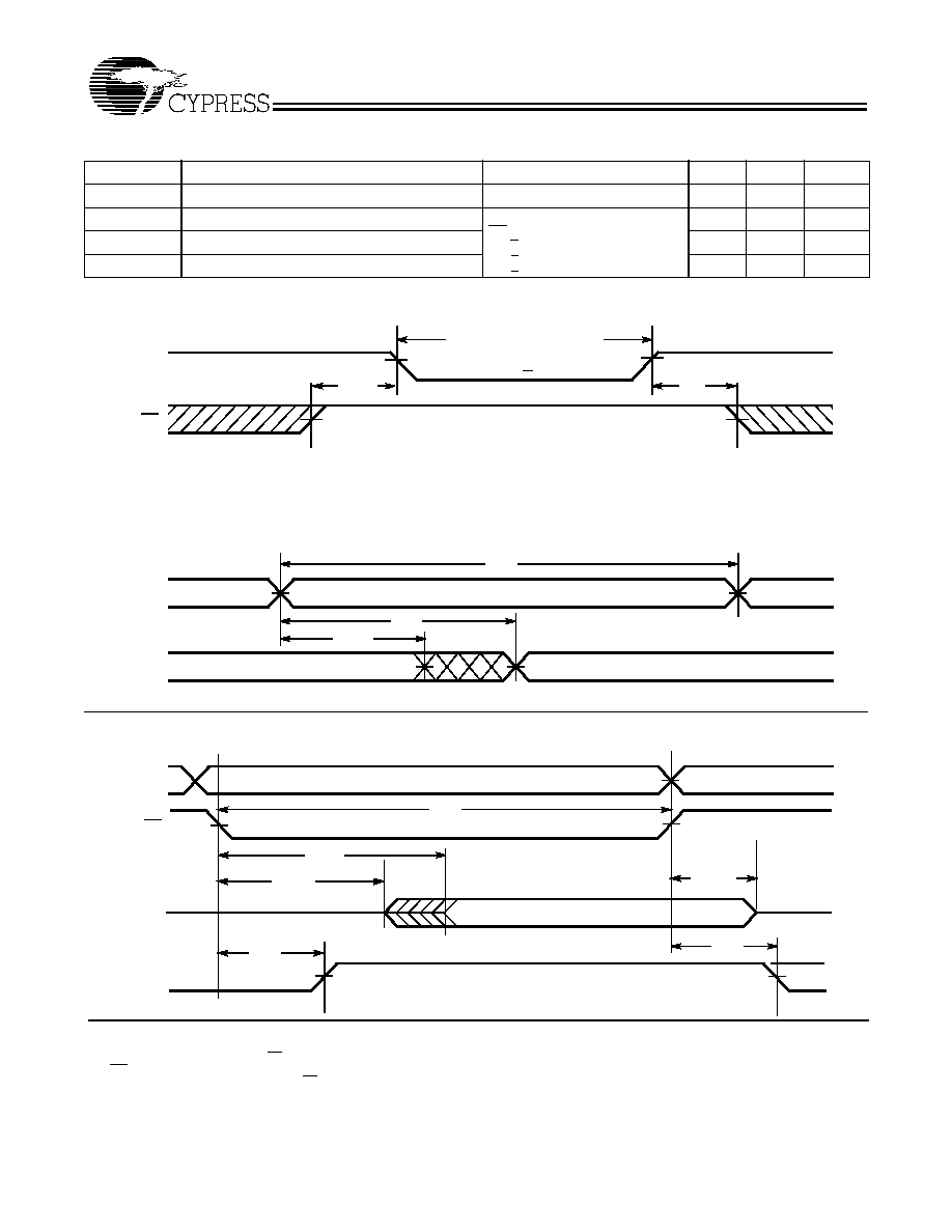
Switching Waveforms
Read Cycle No. 1
[10, 11]
Read Cycle No. 2
[11, 12]
Notes:
9.
No input may exceed V
CC
+ 0.5V.
10. Device is continuously selected, CE = V
IL
.
11. WE is HIGH for read cycle.
12. Address valid prior to or coincident with CE transition LOW.
PREVIOUS DATA VALID
DATA VALID
t
RC
t
AA
t
OHA
107-6
ADDRESS
DATA OUT
50%
50%
DATA VALID
t
RC
t
ACE
t
LZCE
t
PU
HIGH IMPEDANCE
t
HZCE
t
PD
HIGH
ICC
ISB
IMPEDANCE
ADDRESS
CE
DATA OUT
V
CC
SUPPLY
CURRENT
107-7