128K x 8 Static RAM
CY7C109
CY7C1009
Cypress Semiconductor Corporation
∑
3901 North First Street
∑
San Jose
∑
CA 95134
∑
408-943-2600
Document #: 38-05032 Rev. **
Revised August 24, 2001
009
Features
∑ High speed
-- t
AA
= 10 ns
∑ Low active power
-- 1017 mW (max., 12 ns)
∑ Low CMOS standby power
-- 55 mW (max.), 4 mW (Low power version)
∑ 2.0V Data Retention (Low power version)
∑ Automatic power-down when deselected
∑ TTL-compatible inputs and outputs
∑ Easy memory expansion with CE
1
, CE
2
, and OE options
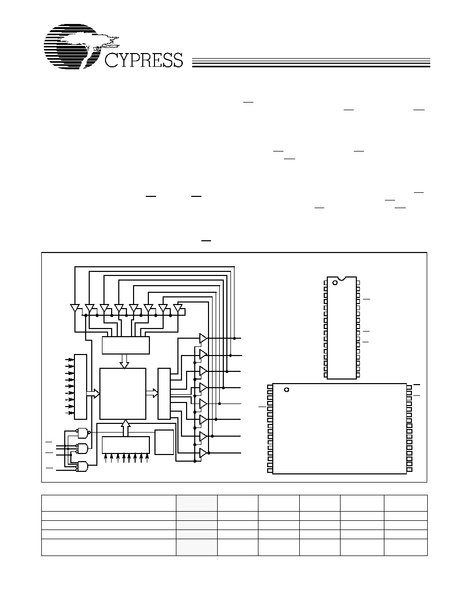
Functional Description
The CY7C109 / CY7C1009 is a high-performance CMOS stat-
ic RAM organized as 131,072 words by 8 bits. Easy memory
expansion is provided by an active LOW chip enable (CE
1
), an
active HIGH chip enable (CE
2
), an active LOW output enable
(OE), and three-state drivers. Writing to the device is accom-
plished by taking chip enable one (CE
1
) and write enable (WE)
inputs LOW and chip enable two (CE
2
) input HIGH. Data on
the eight I/O pins (I/O
0
through I/O
7
) is then written into the
location specified on the address pins (A
0
through A
16
).
Reading from the device is accomplished by taking chip en-
able one (CE
1
) and output enable (OE) LOW while forcing
write enable (WE) and chip enable two (CE
2
) HIGH. Under
these conditions, the contents of the memory location speci-
fied by the address pins will appear on the I/O pins.
The eight input/output pins (I/O
0
through I/O
7
) are placed in a
high-impedance state when the device is deselected (CE
1
HIGH or CE
2
LOW), the outputs are disabled (OE HIGH), or
during a write operation (CE
1
LOW, CE
2
HIGH, and WE LOW).
The CY7C109 is available in standard 400-mil-wide SOJ and
32-pin TSOP type I packages. The CY7C1009 is available in
a 300-mil-wide SOJ package. The CY7C1009 and CY7C109
are functionally equivalent in all other respects.
14
15
Logic Block Diagram
Pin Configurations
A
1
A
2
A
3
A
4
A
5
A
6
A
7
A
8
COLUMN
DECODER
ROW DECODER
SENS
E AM
PS
INPUT BUFFER
POWER
DOWN
WE
OE
I/O
0
CE
2
I/O
1
I/O
2
I/O
3
512 x 256 x 8
ARRAY
I/O
7
I/O
6
I/O
5
I/O
4
A
0
A
11
A
13
A
12
A
A
10
CE
1
A
A
16
A
9
1
2
3
4
5
6
7
8
9
10
11
14
19
20
24
23
22
21
25
28
27
26
Top View
SOJ
12
13
29
32
31
30
16
15
17
18
GND
A
16
A
14
A
12
A
7
A
6
A
5
A
4
A
3
WE
V
CC
A
15
A
13
A
8
A
9
I/O
7
I/O
6
I/O
5
I/O
4
109≠1
A
2
NC
I/O
0
I/O
1
I/O
2
CE
1
OE
A
10
I/O
3
A
1
A
0
A
11
CE
2
109≠2
A
6
A
7
A
16
A
14
A
12
WE
V
CC
A
4
A
13
A
8
A
9
OE
TSOP I
Top View
(not to scale)
1
6
2
3
4
5
7
32
27
31
30
29
28
26
21
25
24
23
22
19
20
I/O
2
I/O
1
GND
I/O
7
I/O
4
I/O
5
I/O
6
I/O
0
CE
A
11
A
5
17
18
8
9
10
11
12
13
14
15
16
CE
2
A
15
NC
A
10
I/O
3
A
1
A
0
A
3
A
2
109≠3
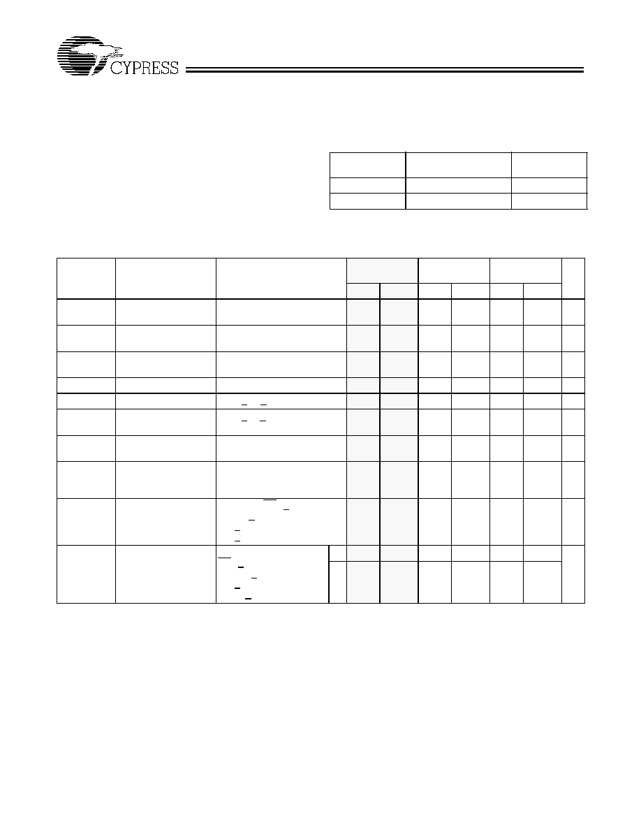
Selection Guide
7C109-10
7C1009-10
7C109-12
7C1009-12
7C109-15
7C1009-15
7C109-20
7C1009-20
7C109-25
7C1009-25
7C109-35
7C1009-35
Maximum Access Time (ns)
10
12
15
20
25
35
Maximum Operating Current (mA)
195
185
155
140
135
125
Maximum CMOS Standby Current (mA)
10
10
10
10
10
10
Maximum CMOS Standby Current (mA)
Low Power Version
2
2
2
--
--
--
Shaded areas contain preliminary information.
CY7C109
CY7C1009
Document #: 38-05032 Rev. **
Page 2 of 12
Maximum Ratings
(Above which the useful life may be impaired. For user guide-
lines, not tested.)
Storage Temperature ................................. ≠65
∞
C to +150
∞
C
Ambient Temperature with
Power Applied............................................. ≠55
∞
C to +125
∞
C
Supply Voltage on V
CC
to Relative GND
[1]
.... ≠0.5V to +7.0V
DC Voltage Applied to Outputs
in High Z State
[1]
....................................≠0.5V to V
CC
+ 0.5V
DC Input Voltage
[1]
................................≠0.5V to V
CC
+ 0.5V
Current into Outputs (LOW) .........................................20 mA
Static Discharge Voltage ........................................... >2001V
(per MIL-STD-883, Method 3015)
Latch-Up Current ..................................................... >200 mA
Operating Range
Range
Ambient
Temperature
[2]
V
CC
Commercial
0
∞
C to +70
∞
C
5V
±
10%
Industrial
-
40
∞
C to +85
∞
C
5V
±
10%
Electrical Characteristics
Over the Operating Range
[3]
Test Conditions
7C109-10
7C1009-10
7C109-12
7C1009-12
7C109-15
7C1009≠15
Parameter
Description
Min.
Max.
Min.
Max.
Min.
Max.
Unit
V
OH
Output HIGH Voltage
V
CC
= Min.,
I
OH
= ≠4.0 mA
2.4
2.4
2.4
V
V
OL
Output LOW Voltage
V
CC
= Min.,
I
OL
= 8.0 mA
0.4
0.4
0.4
V
V
IH
Input HIGH Voltage
2.2
V
CC
+ 0.3
2.2
V
CC
+ 0.3
2.2
V
CC
+ 0.3
V
V
IL
Input LOW Voltage
[1]
≠0.3
0.8
≠0.3
0.8
≠0.3
0.8
V
I
IX
Input Load Current
GND < V
I
< V
CC
≠1
+1
≠1
+1
≠1
+1
µ
A
I
OZ
Output Leakage
Current
GND < V
I
< V
CC
,
Output Disabled
≠5
+5
≠5
+5
≠5
+5
µ
A
I
OS
Output Short
Circuit Current
[3]
V
CC
= Max.,
V
OUT
= GND
≠300
≠300
≠300
mA
I
CC
V
CC
Operating
Supply Current
V
CC
= Max.,
I
OUT
= 0 mA,
f = f
MAX
= 1/t
RC
195
185
155
mA
I
SB1
Automatic CE
Power-Down Current
-- TTL Inputs
Max. V
CC
, CE
1
> V
IH
or CE
2
< V
IL
,
V
IN
> V
IH
or
V
IN
< V
IL
, f = f
MAX
45
45
40
mA
I
SB2
Automatic CE
Power-Down Current
-- CMOS Inputs
Max. V
CC
,
CE
1
> V
CC
≠ 0.3V,
or CE
2
< 0.3V,
V
IN
> V
CC
≠ 0.3V,
or V
IN
< 0.3V, f=0
10
10
10
mA
L
2
2
2
Shaded areas contain preliminary information.
CY7C109
CY7C1009
Document #: 38-05032 Rev. **
Page 3 of 12
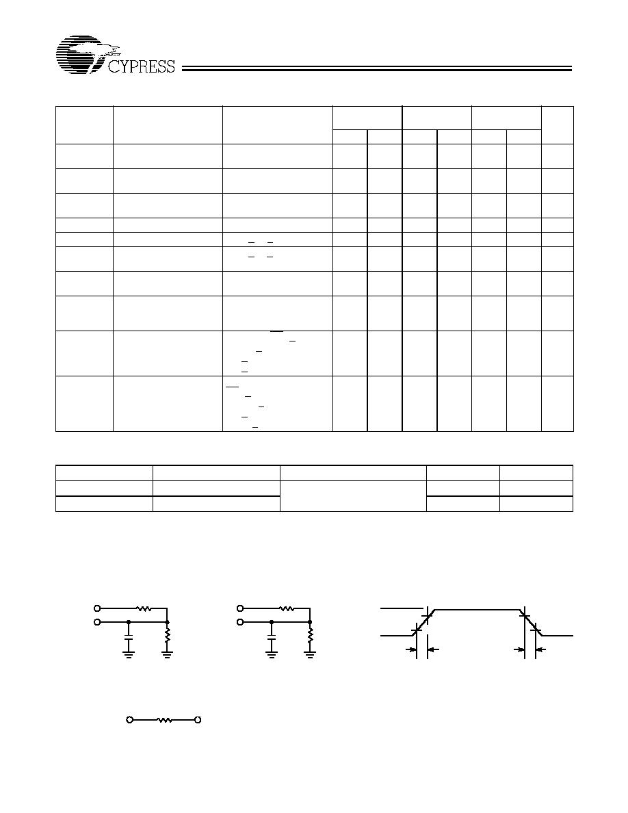
Electrical Characteristics
Over the Operating Range (continued)
7C109-20
7C1009-20
7C109-25
7C1009-25
7C109-35
7C1009-35
Parameter
Description
Test Conditions
Min.
Max.
Min.
Max.
Min.
Max.
Unit
V
OH
Output HIGH Voltage
V
CC
= Min.,
I
OH
= ≠4.0 mA
2.4
2.4
2.4
V
V
OL
Output LOW Voltage
V
CC
= Min.,
I
OL
= 8.0 mA
0.4
0.4
0.4
V
V
IH
Input HIGH Voltage
2.2
V
CC
+ 0.3
2.2
V
CC
+ 0.3
2.2
V
CC
+ 0.3
V
V
IL
Input LOW Voltage
[1]
≠0.3
0.8
≠0.3
0.8
≠0.3
0.8
V
I
IX
Input Load Current
GND < V
I
< V
CC
≠1
+1
≠1
+1
≠1
+1
µ
A
I
OZ
Output Leakage
Current
GND < V
I
< V
CC
,
Output Disabled
≠5
+5
≠5
+5
≠5
+5
µ
A
I
OS
Output Short
Circuit Current
[3]
V
CC
= Max.,
V
OUT
= GND
≠300
≠300
≠300
mA
I
CC
V
CC
Operating
Supply Current
V
CC
= Max.,
I
OUT
= 0 mA,
f = f
MAX
= 1/t
RC
140
135
125
mA
I
SB1
Automatic CE
Power-Down Current
-- TTL Inputs
Max. V
CC
, CE
1
> V
IH
or CE
2
< V
IL
,
V
IN
> V
IH
or
V
IN
< V
IL
, f = f
MAX
30
30
25
mA
I
SB2
Automatic CE
Power-Down Current
-- CMOS Inputs
Max. V
CC
,
CE
1
> V
CC
≠ 0.3V,
or CE
2
< 0.3V,
V
IN
> V
CC
≠ 0.3V,
or V
IN
< 0.3V, f=0
10
10
10
mA
Capacitance
[4]
Parameter
Description
Test Conditions
Max.
Unit
C
IN
Input Capacitance
T
A
= 25
∞
C, f = 1 MHz,
V
CC
= 5.0V
9
pF
C
OUT
Output Capacitance
8
pF
Notes:
1.
V
IL
(min.) = ≠2.0V for pulse durations of less than 20 ns.
2.
T
A
is the "instant on" case temperature.
3.
Not more than one output should be shorted at one time. Duration of the short circuit should not exceed 30 seconds.
4.
Tested initially and after any design or process changes that may affect these parameters.
AC Test Loads and Waveforms
109≠3
109≠4
90%
10%
3.0V
GND
90%
10%
ALL INPUT PULSES
5V
OUTPUT
30 pF
INCLUDING
JIG AND
SCOPE
5V
OUTPUT
5 pF
INCLUDING
JIG AND
SCOPE
(a)
(b)
3ns
3 ns
OUTPUT
R1 480
R1 480
R2
255
R2
255
167
Equivalent to:
VENIN EQUIVALENT
1.73V
TH…
CY7C109
CY7C1009
Document #: 38-05032 Rev. **
Page 4 of 12
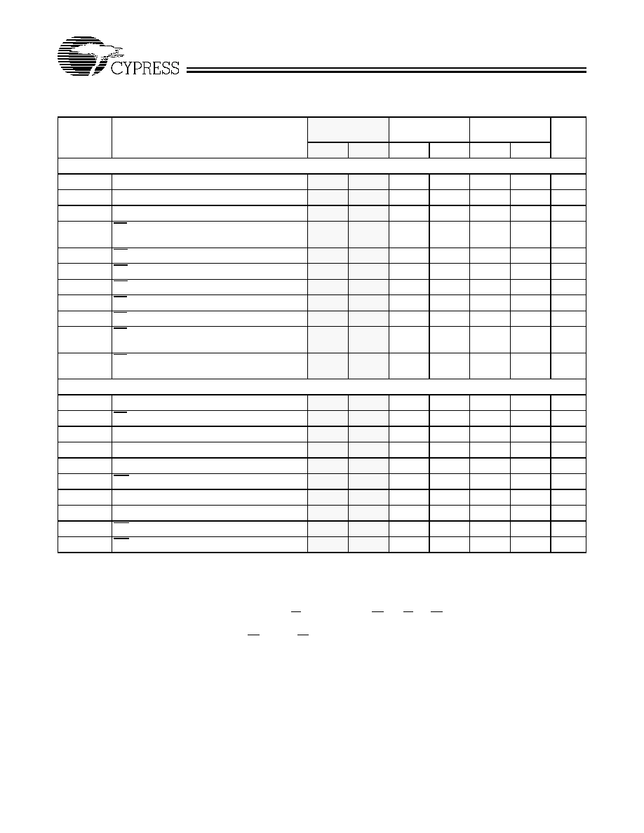
Switching Characteristics
[3, 5]
Over the Operating Range
7C109-10
7C1009-10
7C109-12
7C1009-12
7C109-15
7C1009-15
Parameter
Description
Min.
Max.
Min.
Max.
Min.
Max.
Unit
READ CYCLE
t
RC
Read Cycle Time
10
12
15
ns
t
AA
Address to Data Valid
10
12
15
ns
t
OHA
Data Hold from Address Change
3
3
3
ns
t
ACE
CE
1
LOW to Data Valid, CE
2
HIGH to Data
Valid
10
12
15
ns
t
DOE
OE LOW to Data Valid
5
6
7
ns
t
LZOE
OE LOW to Low Z
0
0
0
ns
t
HZOE
OE HIGH to High Z
[6, 7]
5
6
7
ns
t
LZCE
CE
1
LOW to Low Z, CE
2
HIGH to Low Z
[7]
3
3
3
ns
t
HZCE
CE
1
HIGH to High Z, CE
2
LOW to High Z
[6, 7]
5
6
7
ns
t
PU
CE
1
LOW to Power-Up, CE
2
HIGH to
Power-Up
0
0
0
ns
t
PD
CE
1
HIGH to Power-Down, CE
2
LOW to
Power-Down
10
12
15
ns
WRITE CYCLE
[8,9]
t
WC
Write Cycle Time
10
12
15
ns
t
SCE
CE
1
LOW to Write End, CE
2
HIGH to Write End
8
10
12
ns
t
AW
Address Set-Up to Write End
8
10
12
ns
t
HA
Address Hold from Write End
0
0
0
ns
t
SA
Address Set-Up to Write Start
0
0
0
ns
t
PWE
WE Pulse Width
8
10
12
ns
t
SD
Data Set-Up to Write End
6
7
8
ns
t
HD
Data Hold from Write End
0
0
0
ns
t
LZWE
WE HIGH to Low Z
[7]
3
3
3
ns
t
HZWE
WE LOW to High Z
[6, 7]
5
6
7
ns
Shaded areas contain preliminary information.
Notes:
5.
Test conditions assume signal transition time of 3 ns or less, timing reference levels of 1.5V, input pulse levels of 0 to 3.0V, and output loading of the specified
I
OL
/I
OH
and 30-pF load capacitance.
6.
t
HZOE
, t
HZCE
, and t
HZWE
are specified with a load capacitance of 5 pF as in part (b) of AC Test Loads. Transition is measured
±
500 mV from steady-state voltage.
7.
At any given temperature and voltage condition, t
HZCE
is less than t
LZCE
, t
HZOE
is less than t
LZOE
, and t
HZWE
is less than t
LZWE
for any given device.
8.
The internal write time of the memory is defined by the overlap of CE
1
LOW, CE
2
HIGH, and WE LOW. CE
1
and WE must be LOW and CE
2
HIGH to initiate a write,
and the transition of any of these signals can terminate the write. The input data set-up and hold timing should be referenced to the leading edge of the signal that terminates
the write.
9.
The minimum write cycle time for Write Cycle no. 3 (WE controlled, OE LOW) is the sum of t
HZWE
and T
SD
.
CY7C109
CY7C1009
Document #: 38-05032 Rev. **
Page 5 of 12
Switching Characteristics
[3, 5]
Over the Operating Range
Parameter
Description
7C109-20
7C1009-20
7C109-25
7C1009-25
7C109-35
7C1009-35
Unit
Min.
Max.
Min.
Max.
Min.
Min.
READ CYCLE
t
RC
Read Cycle Time
20
25
35
ns
t
AA
Address to Data Valid
20
25
35
ns
t
OHA
Data Hold from Address Change
3
5
5
ns
t
ACE
CE
1
LOW to Data Valid, CE
2
HIGH to Data
Valid
20
25
35
ns
t
DOE
OE LOW to Data Valid
8
10
15
ns
t
LZOE
OE LOW to Low Z
0
0
0
ns
t
HZOE
OE HIGH to High Z
[6, 7]
8
10
15
ns
t
LZCE
CE
1
LOW to Low Z, CE
2
HIGH to Low Z
[7]
3
5
5
ns
t
HZCE
CE
1
HIGH to High Z, CE
2
LOW to High Z
[6, 7]
8
10
15
ns
t
PU
CE
1
LOW to Power-Up, CE
2
HIGH to
Power-Up
0
0
0
ns
t
PD
CE
1
HIGH to Power-Down, CE
2
LOW to
Power-Down
20
25
35
ns
WRITE CYCLE
[8]
t
WC
Write Cycle Time
20
25
35
ns
t
SCE
CE
1
LOW to Write End, CE
2
HIGH to Write End
15
20
25
ns
t
AW
Address Set-Up to Write End
15
20
25
ns
t
HA
Address Hold from Write End
0
0
0
ns
t
SA
Address Set-Up to Write Start
0
0
0
ns
t
PWE
WE Pulse Width
12
15
20
ns
t
SD
Data Set-Up to Write End
10
15
20
ns
t
HD
Data Hold from Write End
0
0
0
ns
t
LZWE
WE HIGH to Low Z
[7]
3
5
5
ns
t
HZWE
WE LOW to High Z
[6, 7]
8
10
15
ns
Data Retention Characteristics
Over the Operating Range (L Version Only)
Parameter
Description
Conditions
Min.
Max
Unit
V
DR
V
CC
for Data Retention
No input may exceed V
CC
+ 0.5V
V
CC
= V
DR
= 2.0V,
CE
1
> V
CC
≠ 0.3V or CE
2
< 0.3V,
V
IN
> V
CC
≠ 0.3V or V
IN
< 0.3V
2.0
V
I
CCDR
Data Retention Current
50
µ
A
t
CDR
Chip Deselect to Data Retention Time
0
ns
t
R
Operation Recovery Time
t
RC
ns
Shaded areas contain preliminary information.