Äîêóìåíòàöèÿ è îïèñàíèÿ www.docs.chipfind.ru
1-Mb (32K x 32) Pipelined Sync SRAM
CY7C1215F
Cypress Semiconductor Corporation
·
3901 North First Street
·
San Jose
,
CA 95134
·
408-943-2600
Document #: 38-05421 Rev. **
Revised January 26, 2004
Features
· Registered inputs and outputs for pipelined operation
· 32K × 32 common I/O architecture
· 3.3V core power supply
· 3.3V I/O operation
· Fast clock-to-output times
-- 3.5ns (for 166-MHz device)
-- 4.0 ns (for 133-MHz device)
· Provide high-performance 3-1-1-1 access rate
· User-selectable burst counter supporting Intel
Pentium
®
interleaved or linear burst sequences
· Separate processor and controller address strobes
· Synchronous self-timed writes
· Asynchronous output enable
· Offered in JEDEC-standard 100-pin TQFP package
· "ZZ" Sleep Mode Option
Functional Description
[1]
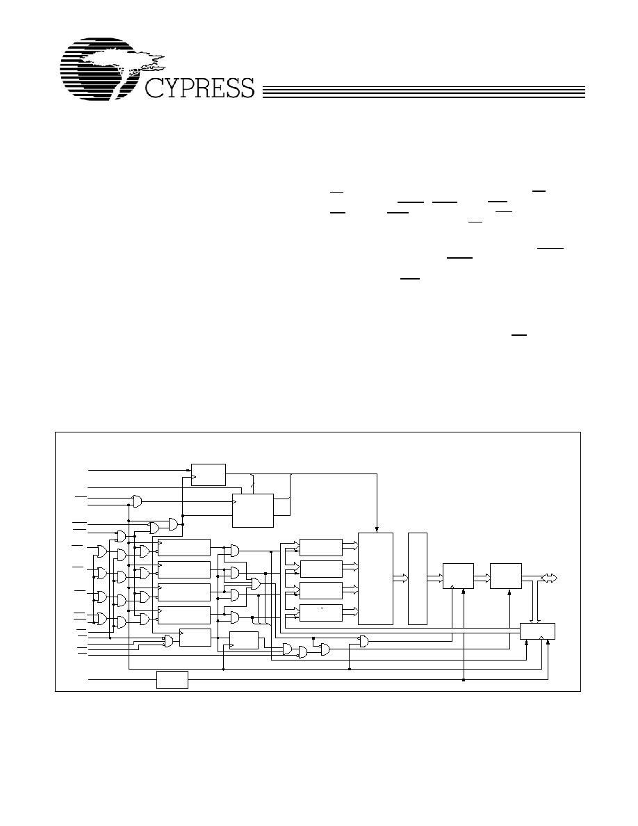
The CY7C1215F SRAM integrates 32,768 x 32 SRAM cells
with advanced synchronous peripheral circuitry and a two-bit
counter for internal burst operation. All synchronous inputs are
gated by registers controlled by a positive-edge-triggered
Clock Input (CLK). The synchronous inputs include all
addresses, all data inputs, address-pipelining Chip Enable
(CE
1
), depth-expansion Chip Enables (CE
2
and
CE
3
), Burst
Control inputs (ADSC, ADSP, and ADV), Write Enables
(BW
[A:D]
, and BWE), and Global Write (GW). Asynchronous
inputs include the Output Enable (OE) and the ZZ pin.
Addresses and chip enables are registered at rising edge of
clock when either Address Strobe Processor (ADSP) or
Address Strobe Controller (ADSC) are active. Subsequent
burst addresses can be internally generated as controlled by
the Advance pin (ADV).
Address, data inputs, and write controls are registered on-chip
to initiate a self-timed Write cycle.This part supports Byte Write
operations (see Pin Descriptions and Truth Table for further
details). Write cycles can be one to four bytes wide as
controlled by the Byte Write control inputs. GW when active
LOW causes all bytes to be written.
The CY7C1215F operates from a +3.3V core power supply
while all outputs may operate with a +3.3V supply. All inputs
and outputs are JEDEC-standard JESD8-5-compatible.
1
Note:
1. For best-practices recommendations, please refer to the Cypress application note System Design Guidelines on www.cypress.com.
Logic Block Diagram
ADDRESS
REGISTER
ADV
CLK
BURST
COUNTER
AND
LOGIC
CLR
Q1
Q0
ADSP
ADSC
MODE
BWE
GW
CE
1
CE
2
CE
3
OE
ENABLE
REGISTER
OUTPUT
REGISTERS
SENSE
AMPS
OUTPUT
BUFFERS
E
PIPELINED
ENABLE
INPUT
REGISTERS
A0, A1, A
BW
B
BW
C
BW
D
BW
A
MEMORY
ARRAY
D Q s
SLEEP
CONTROL
ZZ
A
[1:0]
2
DQ
A
BYTE
WRITE REGISTER
DQ
B
BYTE
WRITE REGISTER
DQ
C
BYTE
WRITE REGISTER
DQ
D
BYTE
WRITE REGISTER
DQ
A
BYTE
WRITE DRIVER
DQ
B
BYTE
WRITE DRIVER
DQ
C
BYTE
WRITE DRIVER
DQ
D
BYTE
WRITE DRIVER
CY7C1215F
Document #: 38-05421 Rev. **
Page 2 of 16
Pin Configuration
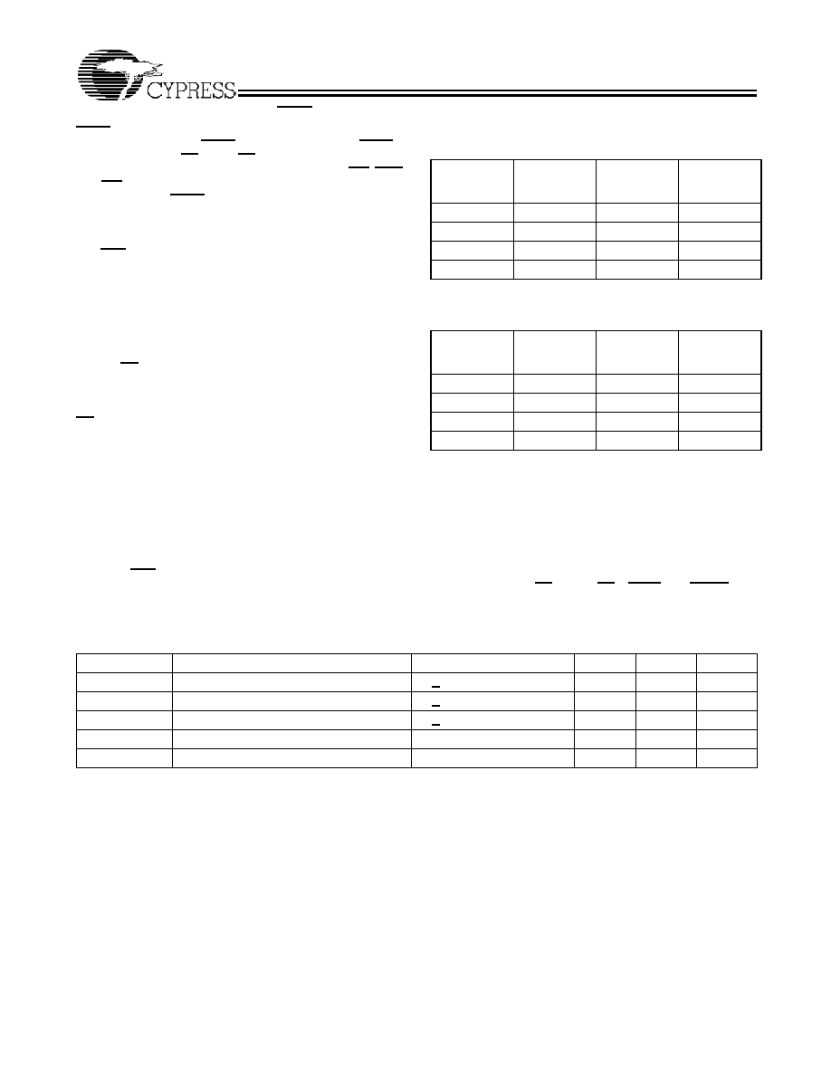
Selection Guide
166 MHz
133 MHz
Unit
Maximum Access Time
3.5
4.0
ns
Maximum Operating Current
240
225
mA
Maximum CMOS Standby Current
40
40
mA
A
A
A
A
A
1
A
0
NC
NC
V
SS
V
DD
NC
NC
A
A
A
A
A
NC
NC
NC
DQ
B
DQ
B
V
DDQ
V
SSQ
DQ
B
DQ
B
DQ
B
DQ
B
V
SSQ
V
DDQ
DQ
B
DQ
B
V
SS
NC
V
DD
ZZ
DQ
A
DQ
A
V
DDQ
V
SSQ
DQ
A
DQ
A
DQ
A
DQ
A
V
SSQ
V
DDQ
DQ
A
DQ
A
NC
NC
DQ
C
DQ
C
V
DDQ
V
SSQ
DQ
C
DQ
C
DQ
C
DQ
C
V
SSQ
V
DDQ
DQ
C
DQ
C
NC
V
DD
NC
V
SS
DQ
D
DQ
D
V
DDQ
V
SSQ
DQ
D
DQ
D
DQ
D
DQ
D
V
SSQ
V
DDQ
DQ
D
DQ
D
NC
A
A
CE
1
CE
2
BW
D
BW
C
BW
B
BW
A
CE
3
V
DD
V
SS
CLK
GW
BWE
OE
ADSC
ADSP
ADV
A
A
1
2
3
4
5
6
7
8
9
10
11
12
13
14
15
16
17
18
19
20
21
22
23
24
25
26
27
28
29
30
31
32
33
34
35
36
37
38
39
40
41
42
43
44
45
46
47
48
49
50
80
79
78
77
76
75
74
73
72
71
70
69
68
67
66
65
64
63
62
61
60
59
58
57
56
55
54
53
52
51
100
99
98
97
96
95
94
93
92
91
90 89
88
87
86
85
84
83
82
81
MOD
E
BYTE A
BYTE B
BYTE D
BYTE C
100-pin TQFP
CY7C1215F
CY7C1215F
Document #: 38-05421 Rev. **
Page 3 of 16
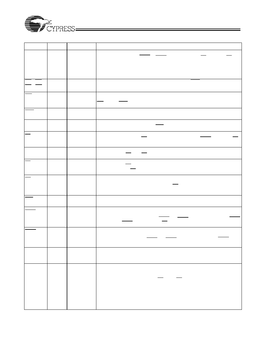
Pin Definitions
Name
TQFP
I/O
Description
A
0
, A
1
, A
37,36,
32,33,34,
35,44,45,
46,47,48,
81,82,99,
100
Input-
Synchronous
Address Inputs used to select one of the 32K address locations. Sampled at the
rising edge of the CLK if ADSP or ADSC is active LOW, and CE
1
,
CE
2
, and
CE
3
are
sampled active. A
1
, A
0
feed the 2-bit counter.
BW
A
,
BW
B
BW
C
,
BW
D
93,94,95,
96
Input-
Synchronous
Byte Write Select Inputs, active LOW. Qualified with BWE to conduct Byte Writes
to the SRAM. Sampled on the rising edge of CLK.
GW
88
Input-
Synchronous
Global Write Enable Input, active LOW. When asserted LOW on the rising edge of
CLK, a global Write is conducted (ALL bytes are written, regardless of the values on
BW
[A:D]
and BWE).
BWE
87
Input-
Synchronous
Byte Write Enable Input, active LOW. Sampled on the rising edge of CLK. This
signal must be asserted LOW to conduct a byte write.
CLK
89
Input-
Clock
Clock Input. Used to capture all synchronous inputs to the device. Also used to
increment the burst counter when ADV is asserted LOW, during a burst operation.
CE
1
98
Input-
Synchronous
Chip Enable 1 Input, active LOW. Sampled on the rising edge of CLK. Used in
conjunction with CE
2
and CE
3
to select/deselect the device. ADSP is ignored if CE
1
is HIGH.
CE
2
97
Input-
Synchronous
Chip Enable 2 Input, active HIGH. Sampled on the rising edge of CLK. Used in
conjunction with CE
1
and CE
3
to select/deselect the device.
CE
3
92
Input-
Synchronous
Chip Enable 3 Input, active LOW. Sampled on the rising edge of CLK. Used in
conjunction with CE
1
and
CE
2
to select/deselect the device. Not connected for BGA.
Where referenced, CE
3
is assumed active throughout this document for BGA.
OE
86
Input-
Asynchronous
Output Enable, asynchronous input, active LOW. Controls the direction of the I/O
pins. When LOW, the I/O pins behave as outputs. When deasserted HIGH, I/O pins
are three-stated, and act as input data pins. OE is masked during the first clock of a
Read cycle when emerging from a deselected state.
ADV
83
Input-
Synchronous
Advance Input signal, sampled on the rising edge of CLK, active LOW. When
asserted, it automatically increments the address in a burst cycle.
ADSP
84
Input-
Synchronous
Address Strobe from Processor, sampled on the rising edge of CLK, active
LOW. When asserted LOW, A is captured in the address registers. A
1
, A
0
are also
loaded into the burst counter. When ADSP and ADSC are both asserted, only ADSP
is recognized. ASDP is ignored when CE
1
is deasserted HIGH.
ADSC
85
Input-
Synchronous
Address Strobe from Controller, sampled on the rising edge of CLK, active LOW.
When asserted LOW, A is captured in the address registers. A
1
, A
0
are also loaded
into the burst counter. When ADSP and ADSC are both asserted, only ADSP is rec-
ognized.
ZZ
64
Input-
Asynchronous
ZZ "Sleep" Input, active HIGH. This input, when HIGH places the device in a
non-time-critical "sleep" condition with data integrity preserved. For normal operation,
this pin has to be LOW or left floating. ZZ pin has an internal pull-down.
DQs
52,53,56,
57,58,59,
62,63,68,
69,72,73,
74,75,78,
79,2,3,6,
7,8,9,12,
13,18,19,
22,23,24,
25,28,29
I/O-
Synchronous
Bidirectional Data I/O lines. As inputs, they feed into an on-chip data register that is
triggered by the rising edge of CLK. As outputs, they deliver the data contained in the
memory location specified by "A" during the previous clock rise of the Read cycle. The
direction of the pins is controlled by OE. When OE is asserted LOW, the pins behave
as outputs. When HIGH, DQ are placed in a three-state condition.
CY7C1215F
Document #: 38-05421 Rev. **
Page 4 of 16
Functional Overview
All synchronous inputs pass through input registers controlled
by the rising edge of the clock. All data outputs pass through
output registers controlled by the rising edge of the clock.
The CY7C1215F supports secondary cache in systems
utilizing either a linear or interleaved burst sequence. The
interleaved burst order supports Pentium and i486
processors. The linear burst sequence is suited for processors
that utilize a linear burst sequence. The burst order is user
selectable, and is determined by sampling the MODE input.
Accesses can be initiated with either the Processor Address
Strobe (ADSP) or the Controller Address Strobe (ADSC).
Address advancement through the burst sequence is
controlled by the ADV input. A two-bit on-chip wraparound
burst counter captures the first address in a burst sequence
and automatically increments the address for the rest of the
burst access.
Byte Write operations are qualified with the Byte Write Enable
(BWE) and Byte Write Select (BW
[A:D]
) inputs. A Global Write
Enable (GW) overrides all Byte Write inputs and writes data to
all four bytes. All writes are simplified with on-chip
synchronous self-timed Write circuitry.
Three synchronous Chip Selects (CE
1
, CE
2
, CE
3
) and an
asynchronous Output Enable (OE) provide for easy bank
selection and output three-state control. ADSP is ignored if
CE
1
is HIGH.
Single Read Accesses
This access is initiated when the following conditions are
satisfied at clock rise: (1) ADSP or ADSC is asserted LOW,
(2) CE
1
, CE
2
, CE
3
are all asserted active, and (3) the Write
signals (GW, BWE) are all deserted HIGH. ADSP is ignored if
CE
1
is HIGH. The address presented to the address inputs (A)
is stored into the address advancement logic and the address
register while being presented to the memory array. The corre-
sponding data is allowed to propagate to the input of the output
registers. At the rising edge of the next clock the data is
allowed to propagate through the output register and onto the
data bus within t
CO
if OE is active LOW. The only exception
occurs when the SRAM is emerging from a deselected state
to a selected state, its outputs are always three-stated during
the first cycle of the access. After the first cycle of the access,
the outputs are controlled by the OE signal. Consecutive
single Read cycles are supported. Once the SRAM is
deselected at clock rise by the chip select and either ADSP or
ADSC signals, its output will three-state immediately.
Single Write Accesses Initiated by ADSP
This access is initiated when both of the following conditions
are satisfied at clock rise: (1) ADSP is asserted LOW, and
(2) CE
1
, CE
2
, CE
3
are all asserted active. The address
presented to A is loaded into the address register and the
address advancement logic while being delivered to the
memory array. The Write signals (GW, BWE, and BW
[A:D]
) and
ADV inputs are ignored during this first cycle.
ADSP-triggered Write accesses require two clock cycles to
complete. If GW is asserted LOW on the second clock rise, the
data presented to the DQ inputs is written into the corre-
sponding address location in the memory array. If GW is HIGH,
then the Write operation is controlled by BWE and BW
[A:D]
signals. The CY7C1215F provides Byte Write capability that is
described in the Write Cycle Descriptions table. Asserting the
Byte Write Enable input (BWE) with the selected Byte Write
(BW
[A:D]
) input, will selectively write to only the desired bytes.
Bytes not selected during a Byte Write operation will remain
unaltered. A synchronous self-timed Write mechanism has
been provided to simplify the Write operations.
Because the CY7C1215F is a common I/O device, the Output
Enable (OE) must be deasserted HIGH before presenting data
to the DQ inputs. Doing so will three-state the output drivers.
As a safety precaution, DQs are automatically three-stated
whenever a Write cycle is detected, regardless of the state of
OE.
V
DD
15,41,65,
91
Power Supply Power supply inputs to the core of the device.
V
SS
17,40,67,
90
Ground
Ground for the core of the device.
V
DDQ
4,11,20,
27,54,61,
70,77
I/O Power Sup-
ply
Power supply for the I/O circuitry.
V
SSQ
5,10,21,
26,55,60,
71,76
I/O Ground
Ground for the I/O circuitry.
MODE
31
Input-
Static
Selects Burst Order. When tied to GND selects linear burst sequence. When tied to
V
DD
or left floating selects interleaved burst sequence. This is a strap pin and should
remain static during device operation. Mode Pin has an internal pull-up.
NC
1,14,16,
30,38,39,
42,43,49,
50,51,66,
80
No Connects. Not internally connected to the die.
Pin Definitions
(continued)
Name
TQFP
I/O
Description
CY7C1215F
Document #: 38-05421 Rev. **
Page 5 of 16
Single Write Accesses Initiated by ADSC
ADSC Write accesses are initiated when the following condi-
tions are satisfied: (1) ADSC is asserted LOW, (2) ADSP is
deserted HIGH, (3) CE
1
, CE
2
, CE
3
are all asserted active, and
(4) the appropriate combination of the Write inputs (GW, BWE,
and BW
[A:D]
) are asserted active to conduct a Write to the
desired byte(s). ADSC-triggered Write accesses require a
single clock cycle to complete. The address presented to A is
loaded into the address register and the address
advancement logic while being delivered to the memory array.
The ADV input is ignored during this cycle. If a global Write is
conducted, the data presented to DQ is written into the corre-
sponding address location in the memory core. If a Byte Write
is conducted, only the selected bytes are written. Bytes not
selected during a Byte Write operation will remain unaltered.
A synchronous self-timed Write mechanism has been
provided to simplify the Write operations.
Because the CY7C1215F is a common I/O device, the Output
Enable (OE) must be deasserted HIGH before presenting data
to the DQ inputs. Doing so will three-state the output drivers.
As a safety precaution, DQ are automatically three-stated
whenever a Write cycle is detected, regardless of the state of
OE.
Burst Sequences
The CY7C1215F provides a two-bit wraparound counter, fed
by A
1
, A
0
, that implements either an interleaved or linear burst
sequence. The interleaved burst sequence is designed specif-
ically to support Intel Pentium applications. The linear burst
sequence is designed to support processors that follow a
linear burst sequence. The burst sequence is user selectable
through the MODE input.
Asserting ADV LOW at clock rise will automatically increment
the burst counter to the next address in the burst sequence.
Both Read and Write burst operations are supported.
Sleep Mode
The ZZ input pin is an asynchronous input. Asserting ZZ
places the SRAM in a power conservation "sleep" mode. Two
clock cycles are required to enter into or exit from this "sleep"
mode. While in this mode, data integrity is guaranteed.
Accesses pending when entering the "sleep" mode are not
considered valid nor is the completion of the operation
guaranteed. The device must be deselected prior to entering
the "sleep" mode. CE
1
, CE
2
, CE
3
, ADSP, and ADSC must
remain inactive for the duration of t
ZZREC
after the ZZ input
returns LOW.
Interleaved Burst Address Table
(MODE = Floating or V
DD
)
First
Address
A
1
, A
0
Second
Address
A
1
, A
0
Third
Address
A
1
, A
0
Fourth
Address
A
1
, A
0
00
01
10
11
01
00
11
10
10
11
00
01
11
10
01
00
Linear Burst Address Table
(MODE = GND)
First
Address
A
1
, A
0
Second
Address
A
1
, A
0
Third
Address
A
1
, A
0
Fourth
Address
A
1
, A
0
00
01
10
11
01
10
11
00
10
11
00
01
11
00
01
10
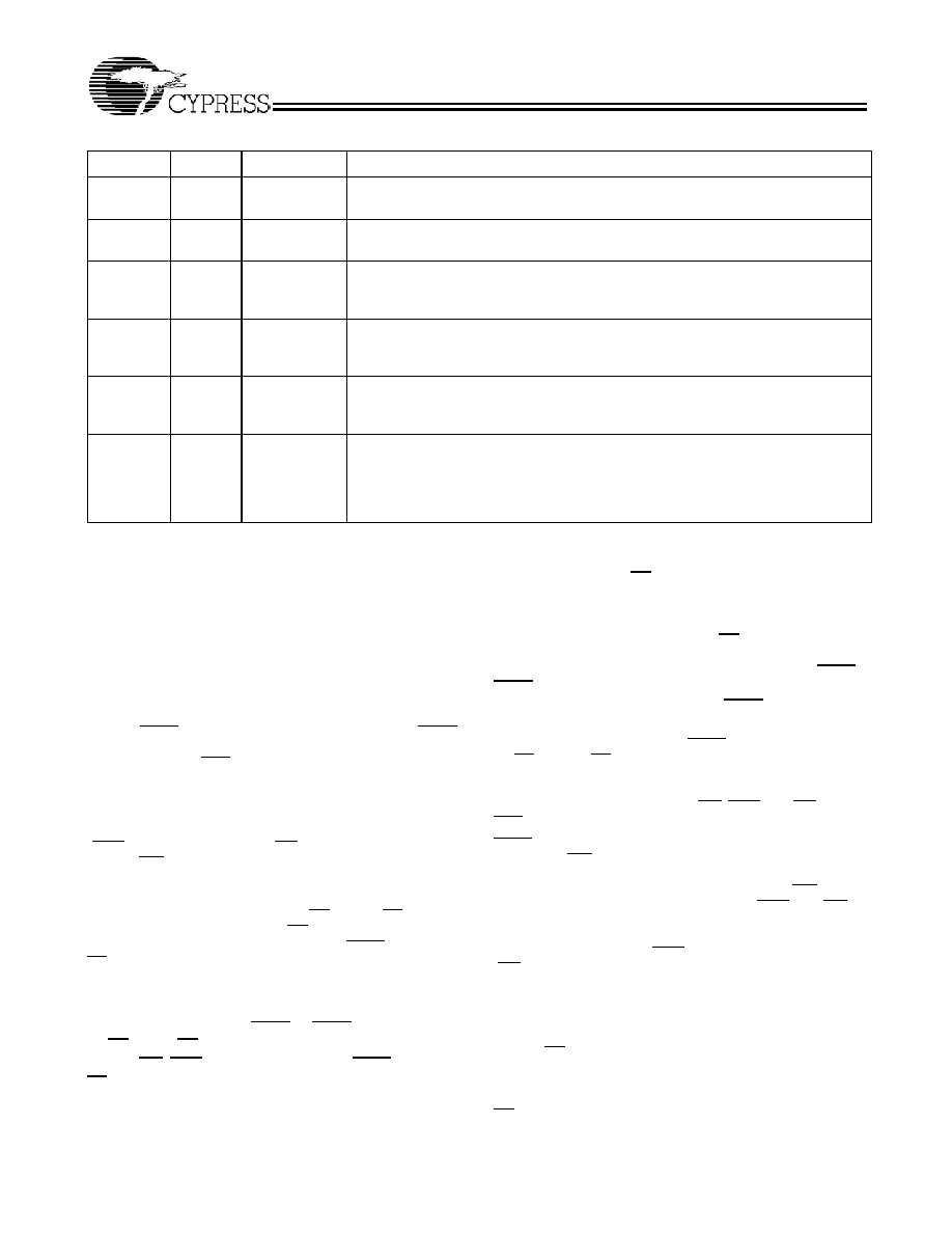
ZZ Mode Electrical Characteristics
Parameter
Description
Test Conditions
Min.
Max.
Unit
I
DDZZ
Snooze mode standby current
ZZ > V
DD
0.2V
40
mA
t
ZZS
Device operation to ZZ
ZZ > V
DD
0.2V
2t
CYC
ns
t
ZZREC
ZZ recovery time
ZZ < 0.2V
2t
CYC
ns
t
ZZI
ZZ Active to snooze current
This parameter is sampled
2t
CYC
ns
t
RZZI
ZZ Inactive to exit snooze current
This parameter is sampled
0
ns