64K x 18 Synchronous Burst RAM
Pipelined Output
CY7C1298A/
GVT7164C18
Cypress Semiconductor Corporation
∑
3901 North First Street
∑
San Jose
∑
CA 95134
∑
408-943-2600
Document #: 38-05194 Rev. *A
Revised January 19, 2003
298A
Features
∑ Fast access times: 5, 6, 7, and 8 ns
∑ Fast clock speed: 100, 83, 66, and 50 MHz
∑ Provide high-performance 3-1-1-1 access rate
∑ Fast OE access times: 5 and 6 ns
∑ Optimal for performance (two cycle chip deselect,
depth expansion without wait state)
∑ Single +3.3V ≠5 to +10% power supply
∑ 5V tolerant inputs except I/Os
∑ Clamp diodes to V
SSQ
at all inputs and outputs
∑ Common data inputs and data outputs
∑ Byte Write Enable and Global Write control
∑ Three chip enables for depth expansion and address
pipeline
∑ Address, control, input, and output pipeline registers
∑ Internally self-timed Write Cycle
∑ Write pass-through capability
∑ Burst control pins (interleaved or linear burst se-
quence)
∑ Automatic power-down for portable applications
∑ High-density, high-speed packages
∑ Low capacitive bus loading
∑ High 30-pF output drive capability at rated access time
Functional Description
The Cypress Synchronous Burst SRAM family employs
high-speed, low-power CMOS designs using advanced dou-
ble-layer polysilicon, double-layer metal technology. Each
memory cell consists of four transistors and two high valued
resistors.
The CY7C1298A/GVT7164C18 SRAM integrates 65536x18
SRAM cells with advanced synchronous peripheral circuitry
and a 2-bit counter for internal burst operation. All synchro-
nous inputs are gated by registers controlled by a posi-
tive-edge-triggered Clock input (CLK). The synchronous in-
puts include all addresses, all data inputs, address-pipelining
Chip Enable (CE), depth-expansion Chip Enables (CE2 and
CE2), burst control inputs (ADSC, ADSP, and ADV), Write En-
ables (WEL, WEH, and BWE), and Global Write (GW).
Asynchronous inputs include the Output Enable (OE) and
Burst Mode Control (MODE). The data outputs (Q), enabled
by OE, are also asynchronous.
Addresses and chip enables are registered with either Ad-
dress Status Processor (ADSP) or Address Status Controller
(ADSC) input pins. Subsequent burst addresses can be inter-
nally generated as controlled by the burst advance pin (ADV).
Address, data inputs, and write controls are registered on-chip
to initiate self-timed Write cycle. Write cycles can be one to
four bytes wide as controlled by the write control inputs. Indi-
vidual byte write allows individual byte to be written. WEL con-
trols DQ1≠DQ8 and DQP1. WEH controls DQ9≠DQ16 and
DQP2. WEL and WEH can be active only with BWE being
LOW. GW being LOW causes all bytes to be written. This de-
vice also incorporates Write pass-through capability and pipe-
lined enable circuit for better system performance.
The CY7C1298A/GVT7164C18 operates from a +3.3V power
supply. All inputs and outputs are TTL-compatible. The device
is ideally suited for 486, PentiumÆ, 680x0, and PowerPCTM
systems and for systems that are benefited from a wide syn-
chronous data bus.
Selection Guide
7C1298A-100
7164C18-5
7C1298A-83
7164C18-6
7C1298A-66
7164C18-7
7C1298A-50
7164C18-8
Maximum Access Time (ns)
5
6
7
8
Maximum Operating Current (mA)
360
315
270
225
Maximum CMOS Standby Current (mA)
2
2
2
2
Pentium is a registered trademark of Intel Corporation.
PowerPC is a trademark of International Business Machines, Inc.
CY7C1298A/
GVT7164C18
Document #: 38-05194 Rev. *A
Page 2 of 12
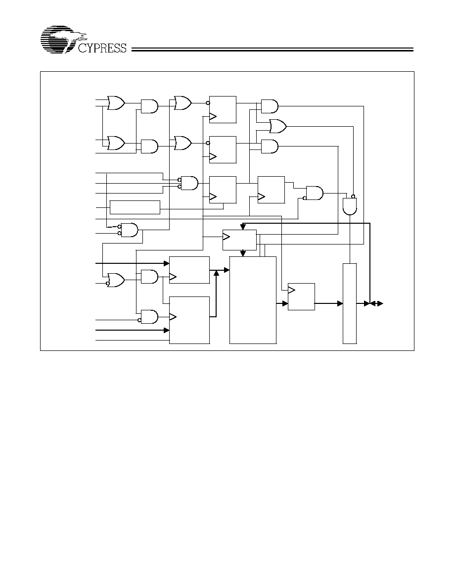
Note:
1.
The Functional Block Diagram illustrates simplified device operation. See Truth Table, pin descriptions and timing diagrams for detailed information.
Functional Block Diagram--64K x 18
[1]
D
Q
D
Q
WEH#
* BWE#
WEL#
* GW#
CE#
* CE2
* CE2#
UPPER BYTE
WRITE
LOWER BYTE
WRITE
OUTPUT
REGISTER
OE#
hi byte write
ADSP#
ADSC#
Address
Register
Binary
Counter
& Logic
CLR
A15-A2
A1-A0
ADV#
* MODE
64K x 9 x 2
S
RAM
Array
Output B
u
ffers
Input
Register
lo byte write
DQ1-
DQ16,
DQP1,
DQP2
D
Q
D
Q
D
Q
ENABLE
Power Down Logic
ZZ
CY7C1298A/
GVT7164C18
Document #: 38-05194 Rev. *A
Page 3 of 12
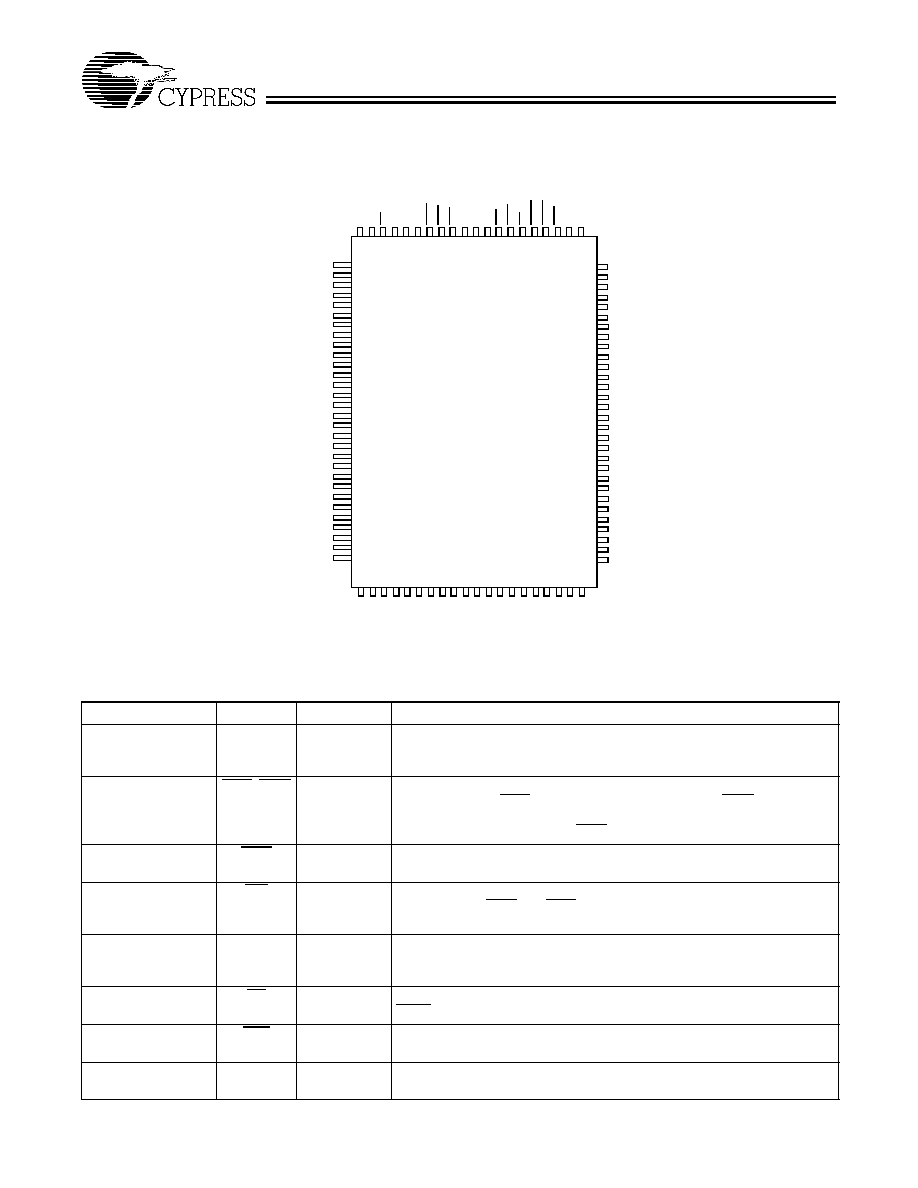
Pin Configuration
100-Pin TQFP
Top View
A10
NC
NC
V
CCQ
V
SSQ
NC
DQP1
DQ8
DQ7
V
SSQ
V
CCQ
DQ6
DQ5
V
SS
NC
V
CC
ZZ
DQ4
DQ3
V
CCQ
V
SSQ
DQ2
DQ1
NC
NC
V
SSQ
V
CCQ
NC
NC
NC
NC
NC
NC
V
CCQ
V
SSQ
NC
NC
DQ9
DQ10
V
SSQ
V
CCQ
DQ11
DQ12
V
CC
NC
V
SS
DQ13
DQ14
V
CCQ
V
SSQ
DQ15
DQ16
DQP2
NC
V
SSQ
V
CCQ
NC
NC
NC
A6
A7
CE
CE2
NC
NC
WEH
WEL
CE2
V
CC
V
SS
CL
K
GW
BW
E
OE
AD
S
C
AD
S
P
AD
V
A8
A9
1
2
3
4
5
6
7
8
9
10
11
12
13
14
15
16
17
18
19
20
21
22
23
24
25
26
27
28
29
30
31
32
33
34
35
36
37
38
39
40
41
42
43
44
45
46
47
48
49
50
80
79
78
77
76
75
74
73
72
71
70
69
68
67
66
65
64
63
62
61
60
59
58
57
56
55
54
53
52
51
10
0
99
98
97
96
95
94
93
92
91
90
89
88
87
86
85
84
83
82
81
CY7C1298A/GVT7164C18
V
CC
A5
A4
A3
A2
A1
A0
NC
NC
V
SS
V
CC
NC
NC
A1
5
A1
4
A1
3
A1
2
A1
1
NC
NC
MOD
E
Pin Descriptions
QFP Pins
Pin Name
Type
Description
37, 36, 35, 34, 33, 32,
100, 99, 82, 81, 80,
48, 47, 46, 45, 44
A0≠A15
Input-
Synchronous
Addresses: These inputs are registered and must meet the set-up and hold
times around the rising edge of CLK. The burst counter generates internal
addresses associated with A0 and A1, during burst cycle and wait cycle.
93, 94
WEL, WEH
Input-
Synchronous
Byte Write Enables: A byte write enable is LOW for a Write cycle and HIGH
for a Read cycle. WEL controls DQ1≠DQ8 and DQP1. WEH controls
DQ9≠DQ16 and DQP2. Data I/O are high-impedance if either of these in-
puts are LOW, conditioned by BWE being LOW.
87
BWE
Input-
Synchronous
Write Enable: This active LOW input gates byte write operations and must
meet the set-up and hold times around the rising edge of CLK.
88
GW
Input-
Synchronous
Global Write: This active LOW input allows a full 18-bit Write to occur inde-
pendent of the BWE and WEn lines and must meet the set-up and hold
times around the rising edge of CLK.
89
CLK
Input-
Synchronous
Clock: This signal registers the addresses, data, chip enables, write control
and burst control inputs on its rising edge. All synchronous inputs must meet
set-up and hold times around the clock's rising edge.
98
CE
Input-
Synchronous
Chip Enable: This active LOW input is used to enable the device and to gate
ADSP.
92
CE2
Input-
Synchronous
Chip Enable: This active LOW input is used to enable the device.
97
CE2
Input-
Synchronous
Chip Enable: This active HIGH input is used to enable the device.
CY7C1298A/
GVT7164C18
Document #: 38-05194 Rev. *A
Page 4 of 12
86
OE
Input
Output Enable: This active LOW asynchronous input enables the data out-
put drivers.
83
ADV
Input-
Synchronous
Address Advance: This active LOW input is used to control the internal burst
counter. A HIGH on this pin generates wait cycle (no address advance).
84
ADSP
Input-
Synchronous
Address Status Processor: This active LOW input, along with CE being
LOW, causes a new external address to be registered and a Read cycle is
initiated using the new address.
85
ADSC
Input-
Synchronous
Address Status Controller: This active LOW input causes device to be de-
selected or selected along with new external address to be registered. A
Read or Write cycle is initiated depending upon write control inputs.
31
MODE
Input-
Static
Mode: This input selects the burst sequence. A LOW on this pin selects
Linear Burst. A NC or HIGH on this pin selects Interleaved Burst.
64
ZZ
Input-
Static
Snooze: LOW or NC for normal operation. HIGH for low-power standby.
58, 59, 62, 63, 68, 69,
72, 73, 8, 9, 12, 13,
18, 19, 22, 23
DQ1≠DQ16
Input/
Output
Data Inputs/Outputs: Low Byte is DQ1≠DQ8. HIgh Byte is DQ9≠DQ16.
Input data must meet set-up and hold times around the rising edge of CLK.
74, 24
DQP1,
DQP2
Input/
Output
Parity Inputs/Outputs: DQP1 is parity bit for DQ1≠DQ8 and DQP2 is parity
bit for DQ9≠DQ16.
14, 15, 41, 65, 91
V
CC
Supply
Power Supply: +3.3V ≠5% and +10%.
17, 40, 67, 90
V
SS
Ground
Ground: GND.
4, 11, 20, 27, 54, 61,
70, 77
V
CCQ
I/O Supply
Output Buffer Supply: +3.3V ≠5% and +10%.
5, 10, 21, 26, 55, 60,
71, 76
V
SSQ
I/O Ground
Output Buffer Ground: GND.
1≠3, 6, 7, 16, 25,
28≠30, 38, 39, 42, 43,
49≠53, 56, 57, 66, 75,
78≠79, 95, 96
NC
-
No Connect: These signals are not internally connected.
Pin Descriptions
(continued)
QFP Pins
Pin Name
Type
Description
Burst Address Table (MODE = NC/V
CC
)
First
Address
(external)
Second
Address
(internal)
Third
Address
(internal)
Fourth
Address
(internal)
A...A00
A...A01
A...A10
A...A11
A...A01
A...A00
A...A11
A...A10
A...A10
A...A11
A...A00
A...A01
A...A11
A...A10
A...A01
A...A00
Burst Address Table (MODE = GND)
First
Address
(external)
Second
Address
(internal)
Third
Address
(internal)
Fourth
Address
(internal)
A...A00
A...A01
A...A10
A...A11
A...A01
A...A10
A...A11
A...A00
A...A10
A...A11
A...A00
A...A01
A...A11
A...A00
A...A01
A...A10
Partial Truth Table for Read/Write
Function
GW
BWE
WEH
WEL
READ
H
H
X
X
READ
H
L
H
H
WRITE one byte
H
L
L
H
WRITE all bytes
H
L
L
L
WRITE all bytes
L
X
X
X
CY7C1298A/
GVT7164C18
Document #: 38-05194 Rev. *A
Page 5 of 12
Notes:
2.
X means "don't care." H means logic HIGH. L means logic LOW. WRITE = L means [BWE + WEL*WEH]*GW equals LOW. WRITE = H means [BWE +
WEL*WEH]*GW equals HIGH.
3.
WEL enables write to DQ1≠DQ8 and DQP1. WEH enables write to DQ9≠DQ16 and DQP2.
4.
All inputs except OE must meet set-up and hold times around the rising edge (LOW to HIGH) of CLK.
5.
Suspending burst generates wait cycle.
6.
For a write operation following a read operation, OE must be HIGH before the input data required set-up time plus High-Z time for OE and staying HIGH throughout
the input data hold time.
7.
This device contains circuitry that will ensure the outputs will be in High-Z during power-up.
8.
ADSP LOW along with chip being selected always initiates a READ cycle at the L-H edge of CLK. A WRITE cycle can be performed by setting WRITE LOW for
the CLK L-H edge of the subsequent wait cycle. Refer to Write timing diagram for clarification.
9.
Previous cycle may be any cycle (non-burst, burst, or wait).
10. BWE is LOW for individual byte WRITE.
11. GW LOW yields the same result for all-byte WRITE operation.
Truth Table
[2, 3, 4, 5, 6, 7, 8]
Operation
Address
Used
CE
CE2
CE2
ADSP
ADSC
ADV
WRITE
OE
CLK
DQ
Deselected Cycle, Power Down
None
H
X
X
X
L
X
X
X
L-H
High-Z
Deselected Cycle, Power Down
None
L
X
L
L
X
X
X
X
L-H
High-Z
Deselected Cycle, Power Down
None
L
H
X
L
X
X
X
X
L-H
High-Z
Deselected Cycle, Power Down
None
L
X
L
H
L
X
X
X
L-H
High-Z
Deselected Cycle, Power Down
None
L
H
X
H
L
X
X
X
L-H
High-Z
READ Cycle, Begin Burst
External
L
L
H
L
X
X
X
L
L-H
Q
READ Cycle, Begin Burst
External
L
L
H
L
X
X
X
H
L-H
High-Z
WRITE Cycle, Begin Burst
External
L
L
H
H
L
X
L
X
L-H
D
READ Cycle, Begin Burst
External
L
L
H
H
L
X
H
L
L-H
Q
READ Cycle, Begin Burst
External
L
L
H
H
L
X
H
H
L-H
High-Z
READ Cycle, Continue Burst
Next
X
X
X
H
H
L
H
L
L-H
Q
READ Cycle, Continue Burst
Next
X
X
X
H
H
L
H
H
L-H
High-Z
READ Cycle, Continue Burst
Next
H
X
X
X
H
L
H
L
L-H
Q
READ Cycle, Continue Burst
Next
H
X
X
X
H
L
H
H
L-H
High-Z
WRITE Cycle, Continue Burst
Next
X
X
X
H
H
L
L
X
L-H
D
WRITE Cycle, Continue Burst
Next
H
X
X
X
H
L
L
X
L-H
D
READ Cycle, Suspend Burst
Current
X
X
X
H
H
H
H
L
L-H
Q
READ Cycle, Suspend Burst
Current
X
X
X
H
H
H
H
H
L-H
High-Z
READ Cycle, Suspend Burst
Current
H
X
X
X
H
H
H
L
L-H
Q
READ Cycle, Suspend Burst
Current
H
X
X
X
H
H
H
H
L-H
High-Z
WRITE Cycle, Suspend Burst
Current
X
X
X
H
H
H
L
X
L-H
D
WRITE Cycle, Suspend Burst
Current
H
X
X
X
H
H
L
X
L-H
D
Pass-Through Truth Table
Previous Cycle
[9]
Present Cycle
Next Cycle
Operation
BWn
Operation
CE
BWn
OE
Operation
Initiate WRITE cycle, all bytes
Address = A(n≠1), data = D(n≠1)
All L
[10, 11]
Initiate READ cycle
Register A(n), Q = D(n≠1)
L
H
L
Read D(n)
Initiate WRITE cycle, all bytes
Address = A(n≠1), data = D(n≠1)
All L
[10, 11]
No new cycle
Q = D(n≠1)
H
H
L
No carry-over from
previous cycle
Initiate WRITE cycle, all bytes
Address = A(n≠1), data = D(n≠1)
All L
[10, 11]
No new cycle
Q = High-Z
H
H
H
No carry-over from
previous cycle
Initiate WRITE cycle, one byte
Address = A(n≠1), data = D(n≠1)
One L
[10]
No new cycle
Q = D(n≠1) for one byte
H
H
L
No carry-over from
previous cycle