 | –≠–ª–µ–∫—Ç—Ä–æ–Ω–Ω—ã–π –∫–æ–º–ø–æ–Ω–µ–Ω—Ç: CY7C1300A | –°–∫–∞—á–∞—Ç—å:  PDF PDF  ZIP ZIP |
128K X 36 Dual I/O Dual Address Synchronous SRAM
CY7C1300A
Cypress Semiconductor Corporation
∑
3901 North First Street
∑
San Jose
∑
CA 95134
∑
408-943-2600
Document #: 38-05075 Rev. *C
Revised January 19, 2003
Features
∑ Fast clock speed: 100 and 83 MHz
∑ Fast access times: 5.0/6.0 ns max.
∑ Single clock operation
∑ Single 3.3V ≠5% and +5% power supply V
CC
∑ Separate V
CCQ
for output buffer
∑ Two chip enables for simple depth expansion
∑ Address, data input, CE1X, CE2X, CE1Y, CE2Y, PTX,
PTY, WEX, WEY, and data output registers on-chip
∑ Concurrent Reads and Writes
∑ Two bidirectional data buses
∑ Can be configured as separate I/O
∑ Pass-through feature
∑ Asynchronous output enables (OEX, OEY)
∑ LVTTL-compatible I/O
∑ Self-timed Write
∑ Automatic power-down
∑ 176-pin TQFP package
Functional Description
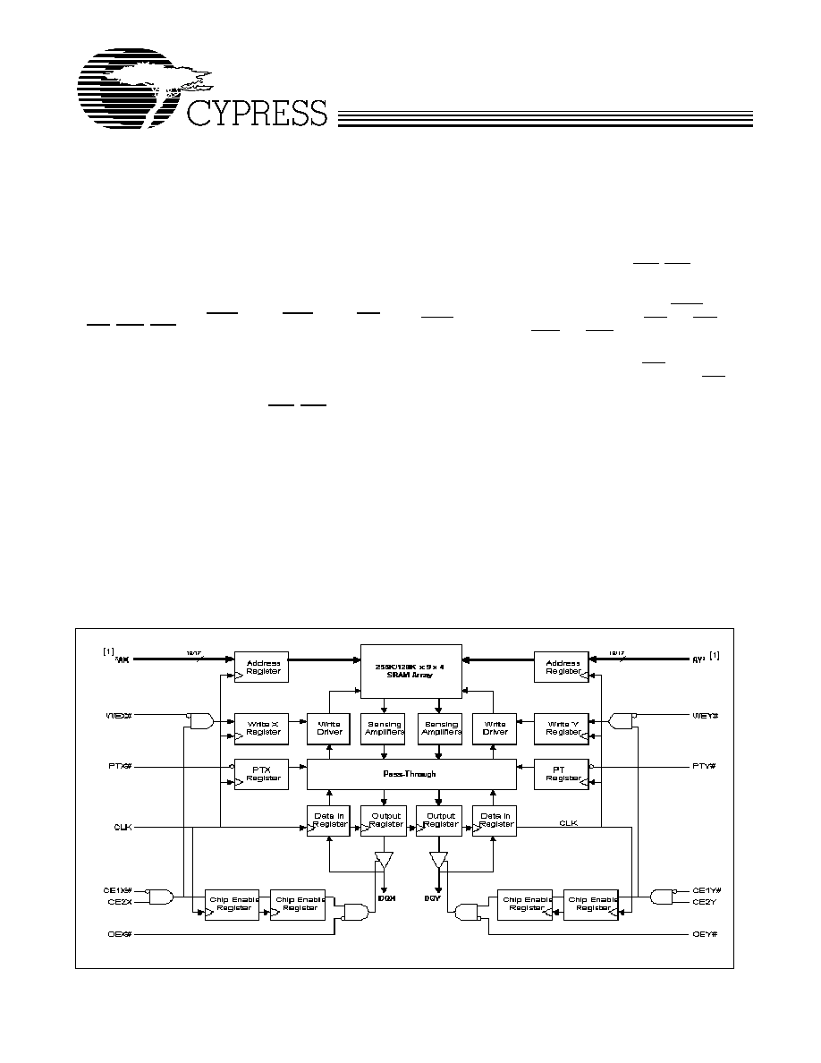
The CY7C1300A SRAM integrates 131,072 ◊ 36 SRAM cells
with advanced synchronous peripheral circuitry. It employs
high-speed, low-power CMOS designs using advanced
triple-layer polysilicon, double-layer metal technology. Each
memory cell consists of four transistors and two high-valued
resistors.
The CY7C1300A allows the user to concurrently perform
Reads, Writes, or pass-through cycles in combination on the
two data ports. The two address ports (AX, AY) determine the
Read or Write locations for their respective data ports (DQX,
DQY).
All input pins except output enable pins (OEX, OEY) are gated
by registers controlled by a positive-edge-triggered clock
(CLK) input. The synchronous inputs include all addresses,
data inputs, depth-expansion chip enables (CE1X, CE2X,
CE1Y and CE2Y), pass-through controls (PTX and PTY), and
Read≠Write control (WEX and WEY).
The pass-through feature allows data to be passed from one
port to another, in either direction. The PTX input must be
asserted to pass data from port X to port Y. The PTY will
likewise pass data from port Y to port X. A pass-through
operation takes precedence over a Read operation.
When AX and AY are the same, certain protocols are followed.
If both ports are Read, the reads occur normally. If one port is
written and the other is read, the read from the array will occur
before the data is written. If both ports are written, only the data
on DQY will be written to the array.
The CY7C1300A operates from a +3.3V power supply. All
inputs and outputs are LVTTL-compatible. These dual I/O,
dual address synchronous SRAMs are well suited for ATM,
Ethernet switches, routers, cell/frame buffers, SNA switches,
and shared memory applications.
The CY7C1300A needs one extra cycle after power for proper
power-on reset. The extra cycle is needed after V
CC
is stable
on the device.
This device is available in a 176-pin TQFP package.
Y
Y
Logic Block Diagram
[1]
Note:
1.
For 128K x 36 devices, AX and AY are 17-bit-wide buses.
CY7C1300A
Document #: 38-05075 Rev. *C
Page 2 of 12
Selection Guide
Pin Configuration
-100
-83
Unit
Maximum access time
5.0
6.0
ns
Maximum operating current
500
430
mA
Maximum CMOS standby current
100
100
mA
Shaded areas contain advance information.
132
VSS
45
VSS
46 47 48 49 50 51 52 53 54 55 56 57 58 59 60 61 62 63 64 65 66 67 68 69 70 71 72 73 74 75 76 77 78 79 80 81 82 83 84 85 86 87 88
44
43
42
41
40
39
38
37
36
35
34
33
32
31
30
29
28
27
26
25
24
23
22
21
20
19
18
17
16
15
14
13
12
11
10
9
8
7
6
5
4
3
2
1
133
131
130
129
128
127
126
125
124
123
122
121
120
119
118
117
116
115
114
113
112
111
110
109
108
107
106
105
104
103
102
101
100
99
98
97
96
95
94
93
92
91
90
89
134
135
136
137
138
139
140
141
142
143
144
145
146
147
148
149
150
151
152
153
154
155
156
157
158
159
160
161
162
163
164
165
166
167
168
169
170
171
172
173
174
175
176
VSS
V
CCQ
DQ
Y
3
5
DQ
X
3
5
VSS
VSS
AY5
AX5
VSS
VC
C
AX1
4
AY1
4
V
CCQ
VSS
DQ
X
1
DQ
Y
1
VSS
DQ
X
0
DQ
Y
0
AX1
3
AY1
3
AX1
2
AY1
2
AX1
1
AY1
1
AX1
0
AY1
0
AY4
AX4
AY3
AX3
AY2
AX2
AY1
AX1
AY0
AX0
DQ
Y
3
4
DQ
X
3
4
DQX20
DQY20
VSS
VCCQ
DQX21
DQY21
DQX22
DQY22
VSS
VCCQ
DQX23
DQY23
DQX24
DQY24
VSS
VCCQ
DQX25
DQY25
DQX26
DQY26
VSS
VCC
DQY27
DQX27
DQY28
DQX28
VSS
VCCQ
DQY29
DQX29
DQY30
DQX30
VSS
VCCQ
DQY31
DQX31
DQY32
DQX32
VSS
VCCQ
DQY33
DQX33
VSS
VSS
DQX15
DQY15
VCCQ
VSS
DQX14
DQY14
DQX13
DQY13
VCCQ
VSS
DQX12
DQY12
DQX11
DQY11
VCCQ
VSS
DQX10
DQY10
DQX9
DQY9
VCC
VSS
DQY8
DQX8
DQY7
DQX7
VCCQ
VSS
DQY6
DQX6
DQY5
DQX5
VCCQ
VSS
DQY4
DQX4
DQY3
DQX3
VCCQ
VSS
DQY2
DQX2
VSS
VSS
VSS
V
CCQ
DQ
Y
1
8
DQ
X
1
8
AX6
AY6
AX7
AY7
VC
C
VSS
AX8
AY8
AX9
VC
C
VSS
DQ
X
1
6
DQ
Y
1
6
VSS
DQ
X
1
7
DQ
Y
1
7
AY9
A
X
17*
A
Y
17*
PT
Y#
PT
X#
WEY#
WEX#
CE
2X
CE
1X
#
OEY#
OEX#
VSS
NC
NC
NC
VSS
NC
NC
CLK
DQ
Y
1
9
DQ
X
1
9
AX1
6
AY1
6
AX1
5
AY1
5
CE
2Y
CE
1Y
#
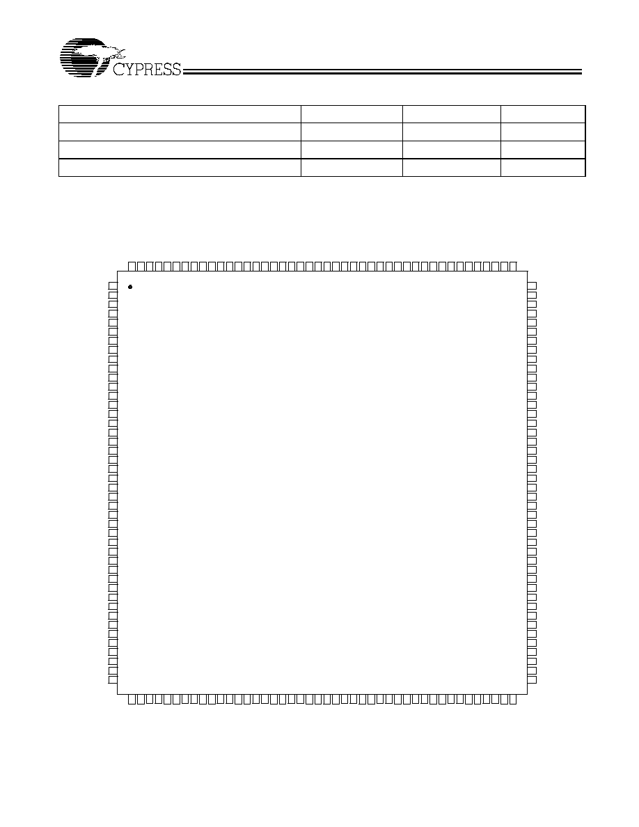
176-pin TQFP
CY7C1300A
Document #: 38-05075 Rev. *C
Page 3 of 12
Pin Definitions
Name
I/O
Description
AX0≠
AX16
Input≠
Synchronous
Synchronous Address Inputs of Port X: Do not allow address pins to float.
AY0≠
AY16
Input≠
Synchronous
Synchronous Address Inputs of Port Y: Do not allow address pins to float.
WEX
Input≠
Synchronous
Read Write of Port X: WEX signal is a synchronous input that identifies whether the current loaded
cycle is a Read or Write operation.
WEY
Input≠
Synchronous
Read Write of Port Y: WEY signal is a synchronous input that identifies whether the current loaded cycle
is a Read or Write operation.
PTX
Input≠
Synchronous
Pass-Through of Port X: PTX signal is a synchronous input that enables passing Port X input to Port
Y output.
PTY
Input≠
Synchronous
Pass-Through of Port Y: PTY signal is a synchronous input that enables passing Port Y input to Port
X output.
OEX
Input
Asynchronous Output Enable of Port X: OEX must be LOW to read data. When OEX is HIGH, the
DQXx pins are in high-impedance state.
OEY
Input
Asynchronous Output Enable of Port Y: OEY must be LOW to read data. When OEY is HIGH, the
DQYx pins are in high-impedance state.
DQX0≠
DQX35
Input/
Output
Data Inputs/Outputs of Port X: Both the data input path and data output path are registered and
triggered by the rising edge of CLK.
DQY0≠
DQY35
Input/
Output
Data Inputs/Outputs of Port Y: Both the data input path and data output path are registered and
triggered by the rising edge of CLK.
CLK
Input≠
Synchronous
Clock: This is the clock input to this device. Except for OEX and OEY, all timing references of the address,
data in, and all control signals for the device are made with respect to the rising edge of CLK.
CE1X
Input≠
Synchronous
Synchronous Active LOW Chip Enable Port X: CE1X is used with CE2X to enable Port X of this
device. CE1X sampled HIGH at the rising edge of clock initiates a deselect cycle for Port X.
CE2X
Input≠
Synchronous
Synchronous Active HIGH Chip Enable Port X: CE2X is used with CE1X to enable Port X of this
device. CE2X sampled LOW at the rising edge of clock initiates a deselect cycle for Port X.
CE1Y
Input≠
Synchronous
Synchronous Active LOW Chip Enable Port Y: CE1Y is used with CE2Y to enable Port Y of this device.
CE1Y sampled HIGH at the rising edge of clock initiates a deselect cycle for Port Y.
CE2Y
Input≠
Synchronous
Synchronous Active HIGH Chip Enable Port Y: CE2Y is used with CE1Y to enable Port Y of this
device. CE2Y sampled LOW at the rising edge of clock initiates a deselect cycle for Port Y.
V
CC
Supply
Power Supply: +3.3V ≠5% and +5%.
V
SS
Ground
Ground: GND.
V
SS
Ground
Ground: GND. No chip current flows through these pins. However, the user needs to connect GND to
these pins.
V
CCQ
I/O Supply
Output Buffer Supply: +3.3V -5% and +5%.
NC
≠
No Connect: These signals are not internally connected. The user can connect them to V
CC
, V
SS
, or
any signal lines, or simply leave them floating.
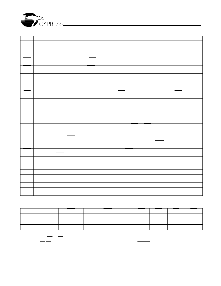
Cycle Description Truth Table
[2, 3, 4, 5, 6, 7, 8, 9]
Operation
CE1X
CE2X
CE1Y
CE2Y
WEX
WEY
PTX
PTY
Deselect Cycle
H
X
H
X
X
X
X
X
Deselect Cycle
X
L
X
L
X
X
X
X
Write Port X
L
H
X
X
0
X
X
X
Notes:
2.
X means "Don't Care." H means logic HIGH. L means logic LOW.
3.
All inputs except OEX and OEY must meet set-up and hold times around the rising edge (LOW to HIGH) of CLK.
4.
OEX and OEY must be asserted to avoid bus contention during Write and Pass-through cycles. For Write and Pass-through operations following a Read
operation, OEX/OEY must be HIGH before the input data required set-up time plus High-Z time for OEX/OEY and staying HIGH throughout the input data
hold time.
5.
Operation numbers 3≠6 can be used in any combination.
6.
Operation numbers 4 and 7, 3 and 8, and 7 and 8 can be combined.
7.
Operation numbers 5 can not be combined with operation number 7 or 8 because Pass-through operation has higher priority over a Read operation.
8.
Operation number 6 can not be combined with operation number 7 or 8 because Pass-through operation has higher priority over a Read operation.
9.
This device contains circuitry that will ensure the outputs will be in High-Z during power-up
CY7C1300A
Document #: 38-05075 Rev. *C
Page 4 of 12
Maximum Ratings
(Above which the useful life may be impaired. For user guide-
lines, not tested.)
Storage Temperature
..................................... -
55∞C to +125∞C
Ambient Temperature with
Power Applied
.................................................... -
10∞C to +85∞C
Supply Voltage on V
DD
Relative to GND
.........-
0.5V to +4.6V
DC Voltage Applied to Outputs
in High-Z State
[10]
...................................-
0.5V to V
CCQ
+ 0.5V
DC Input Voltage
[10]
................................-
0.5V to V
CCQ
+ 0.5V
Current into Outputs (LOW) ........................................ 20 mA
Static Discharge Voltage ......................................... > 1601V
(per MIL-STD-883, Method 3015)
Latch-up Current ................................................... > 200 mA
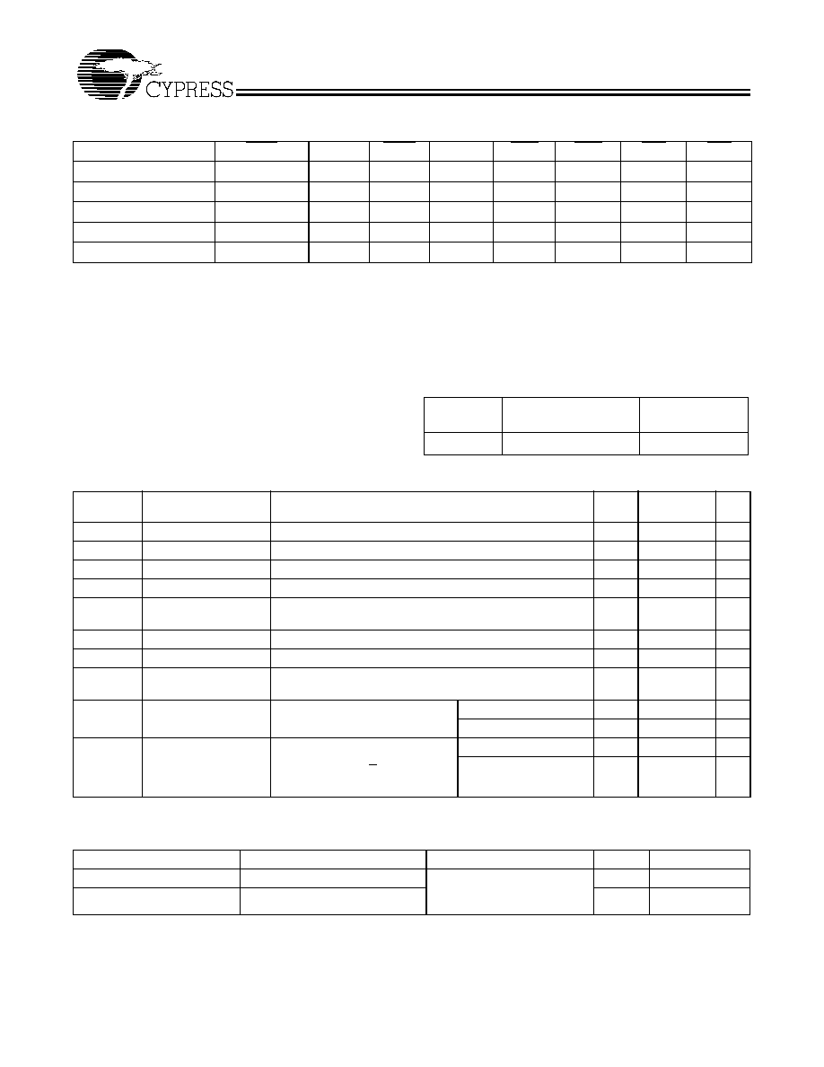
Write Port Y
X
X
L
H
X
0
X
X
Pass-through from X to Y
L
H
L
H
X
X
0
X
Pass-through from Y to X
L
H
L
H
X
X
X
0
Read Port X
L
H
X
X
1
X
1
1
Read Port Y
X
X
L
H
X
1
1
1
Cycle Description Truth Table
(continued)
[2, 3, 4, 5, 6, 7, 8, 9]
Operation
CE1X
CE2X
CE1Y
CE2Y
WEX
WEY
PTX
PTY
Operating Range
Range
Ambient
Temperature
[11]
V
DD
/V
DDQ
(12)
Commercial
0∞C to +70∞C
3.3V ± 5%
Electrical Characteristics
Over the Operating Range
Paramete
r
Description
Test Conditions
Min.
Max.
Unit
V
DD
Power Supply Voltage
3.135
3.465
V
V
DDQ
I/O Supply Voltage
3.135
3.465
V
V
OH
Output HIGH Voltage
V
DD
= Min., I
OH
=
≠4.0 mA
2.4
V
V
OL
Output LOW Voltage
V
DD
= Min., I
OL
= 8.0 mA
0.4
V
V
IH
Input HIGH
Voltage
[13]
2.0
V
CC
+
0.5V
V
V
IL
Input LOW Voltage
[14]
-
0.5
0.8
V
I
X
Input Load Current
GND
V
IN
V
DDQ
-
5
5
µ
A
I
OZ
Output Leakage
Current
GND
V
IN
V
DDQ,
Output Disabled
-
5
5
µ
A
I
CC
V
DD
Operating Supply V
DD
= Max., I
OUT
= 0 mA,
f = f
MAX
= 1/t
CYC
10.0 ns cycle, MHz
500
mA
12.0 ns cycle, 83 MHz
430
mA
I
SB
Automatic CE
Power-down
Current--CMOS
Inputs
Max. V
DD
, Device Deselected
[15]
,
V
IN
0.3V or V
IN
> V
DDQ
≠ 0.3V,
f = 0
10.0 ns cycle, 100 MHz
140
mA
12.0 ns cycle, 83 MHz
120
mA
Capacitance
[16]
Parameter
Description
Test Conditions
Max.
Unit
C
IN
Input
capacitance
T
A
= 25∞C, f = 1 MHz,
V
CC
= 3.3V,
V
CCQ
= 3.3V
8
pF
C
CLK
Clock input capacitance
9
pF
Notes:
10. Minimum voltage equals ≠2.0V for pulse duration less than 20 ns.
11. T
A
is the case temperature.
12. Power supply ramp up should be monotonic.
13. Overshoot: V
IH
+6.0V for t
t
KC /2
.
14. Undershoot: V
IL
≠2.0V for t
t
KC /2
.
15. "Device Deselected" means the device is in power-down mode as defined in the truth table.
16. Tested initially and after any design or process change that may affect these parameters.
CY7C1300A
Document #: 38-05075 Rev. *C
Page 5 of 12
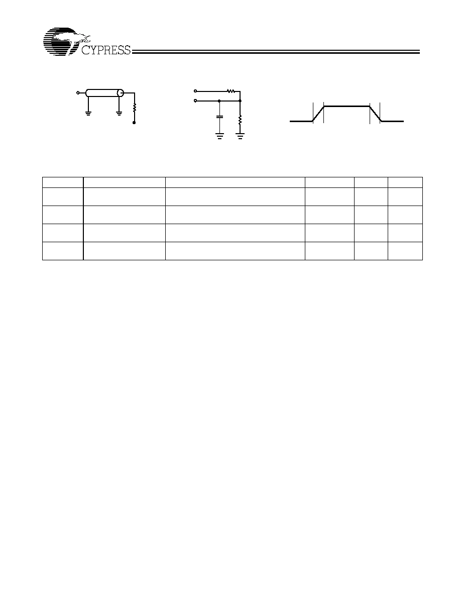
AC Test Loads and Waveforms
[17, 18]
Thermal Resistance
Parameter
Description
Test Conditions
TQFP Typ.
Units
Notes
JA
Thermal Resistance
(Junction to Ambient)
(@200lfm) Single-layer printed circuit board
40
∞
C/W
15
JC
Thermal Resistance
(Junction to Ambient)
(@200lfm) Four-layer printed circuit board
35
∞
C/W
15
JA
Thermal Resistance
(Junction to Board)
Bottom
23
∞
C/W
15
JC
Thermal Resistance
(Junction to Case)
Top
9
∞
C/W
15
Notes:
17. AC test conditions assume a signal transition time of 1 ns or less, timing reference levels of 1.5V, input pulse levels of 0 to 3.0V, and output loading shown in
part (a) of AC Test Loads.
18. Overshoot: VIH(AC) <VDD + 1.5V for t <tTCYC/2; undershoot: VIL(AC) < 0.5V for t <tTCYC/2; power-up: VIH < 2.6V and VDD <2.4V and VDDQ < 1.4V for
t<200 ms.
3.0V
GND
OUTPUT
R = 317
R = 351
5 pF
INCLUDING
JIG AND
SCOPE
(a)
(b)
ALL INPUT PULSES
OUTPUT
R
L
= 50
Z
0
= 50
V
L
= 1.5V
3.3V
[17]
1V/ns
1V/ns
(c)