Untitled Document
9-Mb Pipelined SRAM with QDRTM Architecture
CY7C1302V25
Cypress Semiconductor Corporation
·
3901 North First Street
·
San Jose
,
CA 95134
·
408-943-2600
Document #: 38-05260 Rev. *B
Revised November 12, 2002
Features
· Separate independent read and write data ports
-- Supports concurrent transactions
· 167-MHz clock for high bandwidth
-- 2.5-ns clock-to-valid access time
· Two-word burst on all accesses
· Double data rate (DDR) interfaces on both read and
write ports (data transferred at 333 MHz) @ 167 MHz
· Two input clocks (K and K)
[1]
for precise DDR timing
-- SRAM uses rising edges only
· Two output clocks (C and C) account for clock skew
and flight time mismatches
· Single multiplexed address input bus latches address
inputs for both read and write ports
· Separate port selects for depth expansion
· Synchronous internally self-timed writes
· 2.5V core power supply with HSTL inputs and outputs
[1]
· 13 × 15 mm 1.0-mm pitch FBGA package, 165 ball
(11 × 15 matrix)
· Variable-drive HSTL output buffers
· Expanded HSTL output voltage (1.4V1.9V)
· JTAG interface
· Variable impedance HSTL
Functional Description
The CY7C1302V25 is a 2.5V synchronous pipelined SRAM
with QDRTM architecture. QDR architecture consists of two
separate ports to access the memory array. The Read port has
dedicated Data Outputs to support Read operations and the
Write Port has dedicated Data inputs to support Write opera-
tions. Access to each port is accomplished through a common
address bus. The Read address is latched on the rising edge
of the K
[1]
clock and the Write address is latched on the rising
edge of K
[1]
clock. QDR has separate data inputs and data
outputs to completely eliminate the need to "turn-around" the
data bus required with common I/O devices. Accesses to the
CY7C1302V25 Read and Write ports are completely
independent of one another. All accesses are initiated
synchronously on the rising edge of the positive input clock
(K)
[1]
. In order to maximize data throughput, both Read and
Write ports are equipped with DDR interfaces. Therefore, data
can be transferred into the device on every rising edge of both
input clocks (K and K)
[1]
and out of the device on every rising
edge of the output clock (C and C) thereby maximizing perfor-
mance while simplifying system design.
Depth expansion is accomplished with Port Select inputs for
each port. This allows the ports to operate independently.
All synchronous inputs pass through input registers controlled
by the input clocks (K and K)
[1]
. All data outputs pass through
output registers controlled by the output clocks (C or C). Writes
occur with on-chip synchronous self-timed write circuitry.
Note:
1.
K and K inputs require V
IH
to be greater than V
REF
+ 0.5V and V
IL
to be less than V
REF
0.5V. This is a subset of JEDEC standards for HSTL I/Os.
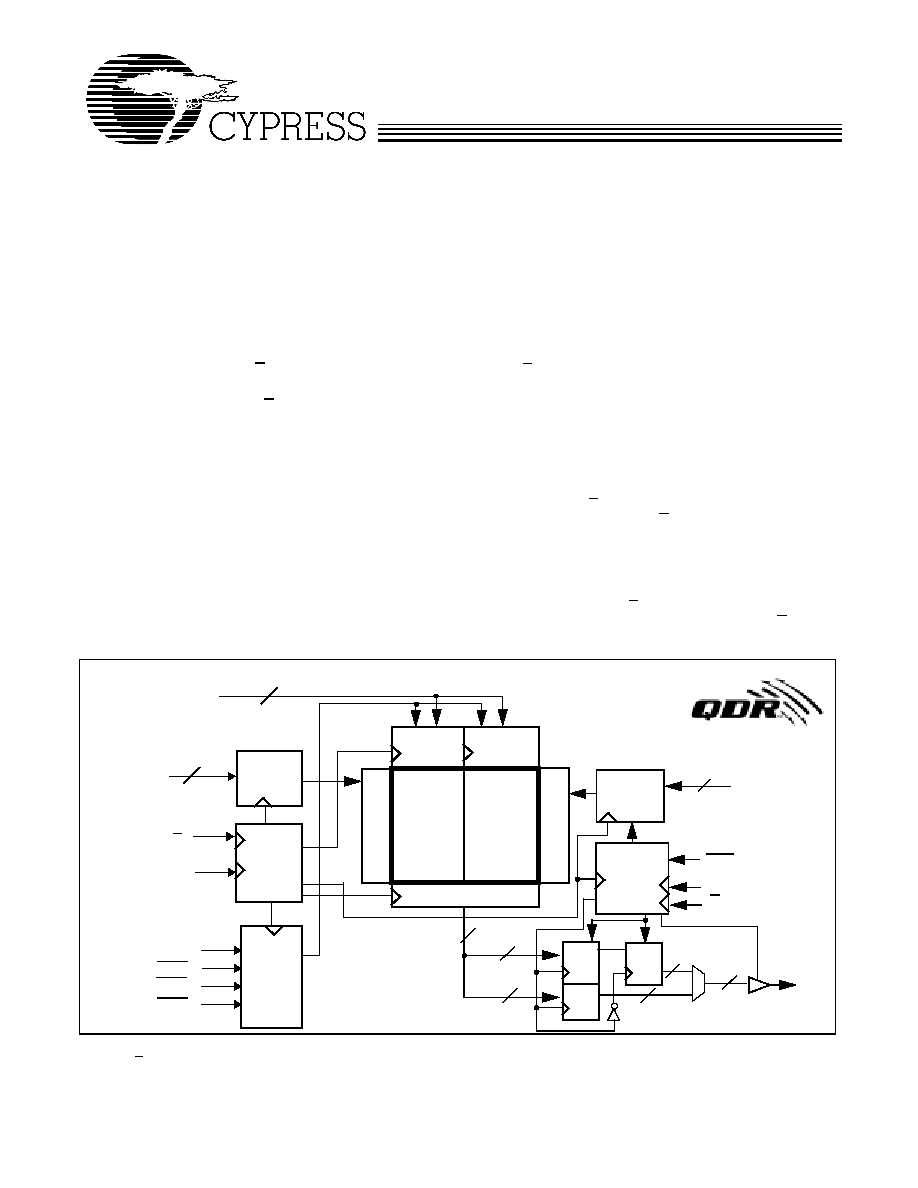
Logic Block Diagram
256Kx18
CLK
A
l17:0]
Gen.
K
[1]
K
[1]
Control
Logic
Address
Register
D
[17:0]
R
ead A
dd.
Decode
Read Data Reg.
RPS
WPS
Q
[17:0]
Control
Logic
Address
Register
Reg.
Reg.
Reg.
18
18
18
36
Write
18
BWS
0
Vref
W
r
it
e Add.
D
e
code
Data Reg
Write
Data Reg
Memory
Array
256Kx18
Memory
Array
18
18
A
[17:0]
18
18
C
C
BWS
1
CY7C1302V25
Document #: 38-05260 Rev. *B
Page 2 of 19
Selection Guide
7C1302V25-167
7C1302V25-133
7C1302V25-100
Maximum Operating Frequency (MHz)
167
133
100
Maximum Operating Current (mA)
550
450
330
Pin Configuration
CY7C1302V25
(Top View)
1
2
3
4
5
6
7
8
9
10
11
A
NC
Gnd/
144M
NC/ 36M
WPS
BWS
1
K
NC
RPS
NC/ 18M
Gnd/
72M
NC
B
NC
Q9
D9
A
NC
K
BWS
0
A
NC
NC
Q8
C
NC
NC
D10
VSS
A
A
A
VSS
NC
Q7
D8
D
NC
D11
Q10
VSS
VSS
VSS
VSS
VSS
NC
NC
D7
E
NC
NC
Q11
VDDQ
VSS
VSS
VSS
VDDQ
NC
D6
Q6
F
NC
Q12
D12
VDDQ
VDD
VSS
VDD
VDDQ
NC
NC
Q5
G
NC
D13
Q13
VDDQ
VDD
VSS
VDD
VDDQ
NC
NC
D5
H
NC
VREF
VDDQ
VDDQ
VDD
VSS
VDD
VDDQ
VDDQ
VREF
ZQ
J
NC
NC
D14
VDDQ
VDD
VSS
VDD
VDDQ
NC
Q4
D4
K
NC
NC
Q14
VDDQ
VDD
VSS
VDD
VDDQ
NC
D3
Q3
L
NC
Q15
D15
VDDQ
VSS
VSS
VSS
VDDQ
NC
NC
Q2
M
NC
NC
D16
VSS
VSS
VSS
VSS
VSS
NC
Q1
D2
N
NC
D17
Q16
VSS
A
A
A
VSS
NC
NC
D1
P
NC
NC
Q17
A
A
C
A
A
NC
D0
Q0
R
TDO
TCK
A
A
A
C
A
A
A
TMS
TDI
Pin Definitions
Name
I/O
Description
D
[17:0]
Input-
Synchronous
Data input signals, sampled on the rising edge of K and K
[1]
clocks during valid
write operations.
WPS
Input-
Synchronous
Write Port Select, active LOW. Sampled on the rising edge of the K
[1]
clock. When
asserted active, a write operation is initiated. Deasserting will deselect the Write port.
Deselecting the Write port will cause D
[17:0]
to be ignored.
BWS
0
, BWS
1
Input-
Synchronous
Byte Write Select 0 and 1, active LOW. Sampled on the rising edge of the K and K
[1]
clocks during write operations. Used to select which byte is written into the device during
the current portion of the write operations. Bytes not written remain unaltered. BWS
0
controls D
[8:0]
while BWS
1
controls D
[17:9].
BWS
0
and BWS
1
are sampled on the same
edge as D
[17:0]
. Deselecting a Byte Write Select will cause the corresponding byte of
data to be ignored and not written into the device.
A
[17:0]
Input-
Synchronous
Address Inputs. Sampled on the rising edge of both the K and K
[1]
clocks during active
read and write operations. These address inputs are multiplexed for both Read and
Write operations. The Read address is latched on the rising edge of the positive input
clock (K)
[1]
and the Write address is latched on the rising edge of the negative input
clock (K)
[1]
. Internally, the device is organized 256K × 36. Therefore, only 18 address
inputs are needed to access the entire memory array. These inputs are ignored when
the appropriate port is deselected. Therefore, on the rising edge of the positive input
clock (K)
[1]
, these inputs are ignored if the Read port is deselected. These inputs are
ignored on the rising edge of the negative input clock (K)
[1]
when the Write port is
deselected.
CY7C1302V25
Document #: 38-05260 Rev. *B
Page 3 of 19
Introduction
Functional Overview
The CY7C1302V25 is a Synchronous Pipelined Burst SRAM
equipped with both a Read Port and a Write Port. The Read
port is dedicated to Read operations and the Write Port is
dedicated to Write operations. Data flows into the SRAM
through the Write port and out through the Read Port. The
CY7C1302V25 multiplexes the address inputs in order to
minimize the number of address pins required. The
CY7C1302V25 latches the Read address on the rising edge
of the positive input clock (K)
[1]
and latches the Write address
on the rising edge of the negative input clock (K)
[1]
. By having
separate Read and Write ports, the CY7C1302V25 completely
eliminates the need to "turn-around" the data bus and avoids
any possible data contention, thereby simplifying system
design.
Q
[17:0]
Outputs-
Synchronous
Data Output Signals. These pins drive out the requested data during a Read operation.
Valid data is driven out on the rising edge of both the C and C clocks during Read
operations. When the Read port is deselected, Q
[17:0]
are automatically three-stated.
RPS
Input-
Synchronous
Read Port Select, active LOW. Sampled on the rising edge of positive input clock (K)
[1]
.
When active, a Read operation is initiated. Deasserting will cause the Read port to be
deselected. When deselected, the pending access is allowed to complete and the output
drivers are automatically three-stated following the next rising edge of the C clock. The
CY7C1302V25 is organized internally as 256K × 36. Each read access consists of a
burst of two sequential 18-bit transfers.
C
Input-
Clock
Positive Output Clock Input. C is used in conjunction with C to clock out the Read
data from the device. C and C can be used together to deskew the flight times of various
devices on the board back to the controller. See application example for further details.
C
Input-
Clock
Negative Output Clock Input. C is used in conjunction with C to clock out the Read
data from the device. C and C can be used together to deskew the flight times of various
devices on the board back to the controller. See application example for further details.
K
Input-
Clock
Positive Input Clock Input. The rising edge of K is used to capture synchronous inputs
to the device and to drive out data through Q
[17:0]
when in single clock mode. All
accesses are initiated on the rising edge of K.
[1]
K
Input-
Clock
Negative Input Clock Input. K is used to capture synchronous inputs being presented
to the device and to drive out data through Q
[17:0]
when in single clock mode.
[1]
ZQ
Input
Output Impedance Matching Input. This input is used to tune the device outputs to
the system data bus impedance. Q
[17:0]
output impedance are set to 0.2 x RQ, where
RQ is a resistor connected between ZQ and ground. Alternately, this pin can be
connected directly to V
DD
, which enables the minimum impedance mode. This pin
cannot be connected directly to GND or left unconnected.
TDO
Output
TDO for JTAG.
TCK
Input
TCK pin for JTAG.
TDI
Input
TDI pin for JTAG.
TMS
Input
TMS pin for JTAG.
NC/18M
Input
Address expansion for 18M. This is not connected to the die.
NC/36M
Input
Address expansion for 36M. This is not connected to the die.
GND/72M
Input
Address expansion for 72M. This should be tied LOW on the CY7C1302V25.
GND/144M
Input
Address expansion for 144M. This should be tied LOW on the CY7C1302V25.
NC
Not Connect Pins. These are not connected to the die.
V
REF
Input-
Reference
Reference Voltage Input. Static input used to set the reference level for HSTL inputs
and Outputs as well as A/C measurement points.
V
DD
Power Supply
Power supply inputs to the core of the device. Should be connected to 2.5V power
supply.
V
SS
Ground
Ground for the device. Should be connected to ground of the system.
V
DDQ
Power Supply
Power supply inputs for the outputs of the device. Should be connected to 1.5V
power supply.
Pin Definitions
(continued)
Name
I/O
Description

CY7C1302V25
Document #: 38-05260 Rev. *B
Page 4 of 19
Accesses for both ports are initiated by the positive input clock
(K)
[1]
. All synchronous input timing is referenced from the
rising edge of the input clocks (K and K)
[1]
and all output timing
is referenced to the output clocks (C and C) or (K and K)
[1]
when in single clock mode.
All synchronous data inputs (D
[17:0]
) inputs pass through input
registers controlled by the input clocks (K and K)
[1]
. All
synchronous data outputs (Q
[17:0]
) outputs pass through
output registers controlled by the rising edge of the output
clocks (C and C)
All synchronous control (RPS, WPS, BWS
0
, BWS
1
) inputs
pass through input registers controlled by the rising edge of
the input clocks (K and K)
[1]
.
Read Operations
Read operations are initiated by asserting RPS active at the
rising edge of the positive input clock (K)
[1]
. The address
presented to A
[17:0]
is stored in the Read address register.
Because the CY7C1302V25 is a 36-bit memory, it will access
two 18-bit data words with each read operation. Following the
next K
[1]
clock rise the data is available to be latched out of the
device, triggered by the C clock. On the following C clock rise
the corresponding lower order word of data is driven onto the
Q
[17:0]
. On the subsequent rising edge of C the higher order
data word is driven onto the Q
[17:0]
. The requested data will be
valid 2.5 ns from the rising edge of the output clock (C or C,
167-MHz device). With the separate Input and Output ports
and the internal logic determining when the device should
drive the data bus, the QDR architecture has eliminated the
need for an output enable input to control the state of the
output drivers.
Read accesses can be initiated on every rising edge of the
Positive Input Clock (K)
[1]
. Doing so will pipeline the data flow
such that data is transferred out of the device on every rising
edge of the output clocks (C and C). The CY7C1302V25 will
deliver the most recent data for the address location being
accessed. This includes forwarding data when a Read and
Write transactions to the same address location are initiated
on the same clock rise.
When the read port is deselected, the CY7C1302V25 will first
complete the pending read transactions. Synchronous internal
circuitry will automatically three-state the outputs following the
next rising edge of the Positive Output Clock (C). This will
allow for a seamless transition between devices without the
insertion of wait states.
The CY7C1302V25 is equipped with internal logic that
synchronously controls the state of the output drivers. The
logic inside the device determines when the output drivers
need to be active or inactive. This advanced logic eliminates
the need for an Asynchronous Output Enable (OE) since the
device will automatically enable/disable the output drivers
during the proper cycles. The CY7C1302V25 will automati-
cally power-up in a deselected state with the outputs in a three
state condition.
Write Operations
Write operations are initiated by asserting WPS active at the
rising edge of the Positive Input Clock (K)
[1]
. On the same
clock rise (K)
[1]
the data presented to D
[17:0]
is stored into the
lower 18-bit Write Data register provided BWS
[1:0]
are both
asserted active. On the subsequent rising edge of the
Negative Input Clock (K)
[1]
, the information presented to A
[17:0]
is latched and stored in the Write Address Register and the
information presented to D
[17:0]
is also stored into the upper
18-bit Write Data Register provided BWS
[1:0]
are both
asserted active. The 36 bits of data are then written into the
memory array at the specified location.
Write accesses can be initiated on every rising edge of the
positive clock. Doing so will pipeline the data flow such that 18
bits of data can be transferred into the device on every rising
edge of the input clocks (K and K)
[1]
.
Byte Write operations are supported by the CY7C1302V25. A
write operation is initiated by selecting the write port using
WPS. The bytes that are written are determined by BWS
0
and
BWS
1
which are sampled with each set of 18-bit data word.
Asserting the appropriate Byte Write Select input during the
data portion of a write will allow the data being presented to be
latched and written into the device. Deasserting the Byte Write
Select input during the data portion of a write will allow the data
stored in the device for that byte to remain unaltered. This
feature can be used to simplify READ/MODIFY/WRITE opera-
tions to a Byte Write operation.
When deselected, the write port will ignore all inputs.
Single Clock Mode
The CY7C1302V25 can be used with a single clock mode. In
this mode the device will recognize only the pair of input clocks
(K and K)
[1]
that control both the input and output registers.
This operation is identical to the operation if the device had
zero skew between the K/K
[1]
and C/C clocks. All timing
parameters remain the same in this mode. To use this mode
of operation, the user must tie C and C to V
DD
. During
power-up, the device will sense the single clock input and
operating in either single clock or double clock mode. The
clock mode should not be changed during device operation.
Concurrent Transactions
The Read and Write ports on the CY7C1302V25 operate
completely independently of one another. Since each port
latches the address inputs on different clock edges, the user
can read or write to any location, regardless of the transaction
on the other port. Should the Read and Write ports access the
same location on the rising edge of the positive input clock, the
information presented to the D
[17:0]
will be forwarded to the
Q
[17:0]
such that no latency is required to access valid data
when operated at or below 100 MHz. Coherency is conducted
on cycle boundaries. Once the second word of data is latched
into the device, the write operation is considered completed.
At this point, any access to that address location will receive
that data until altered by a subsequent Write operation.
Coherency is not maintained for Write operations initiated in
the cycle after a Read.
The data forwarding feature is not
available for operation above 100 MHz
.
Depth Expansion
The CY7C1302V25 has a Port Select input for each port. This
allows for easy depth expansion. Both Port Selects are
sampled on the rising edge of the Positive Input Clock only
(K)
[1]
. Each port select input can deselect the specified port.
Deselecting a port will not affect the other port. All pending
transactions (Read and Write) will be completed prior to the
device being deselected.
CY7C1302V25
Document #: 38-05260 Rev. *B
Page 5 of 19
Programmable Impedance
An external resistor, RQ, must be connected between the ZQ
pin on the SRAM and V
SS
to allow the SRAM to adjust its
output driver impedance. The value of RQ must be 5X the
value of the intended line impedance driven by the SRAM, The
allowable range of RQ to guarantee impedance matching with
a tolerance of ±10% is between 175
and 350
,
with
V
DDQ
=1.5V. The output impedance is adjusted every 1024
cycles to adjust for drifts in supply voltage and temperature.
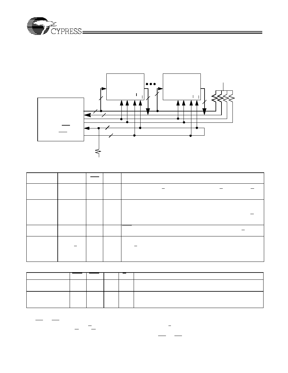
Application Example
Truth Table
[2, 3, 4, 5, 6]
Operation
Address
Used
RPS
K
[1]
Comments
Deselected
H
LH
Read Port is deselected. Outputs three-state following next rising edge of
negative input clock (K)
[1]
if in single clock mode, or C if using C and C as
the output clocks.
Begin Read
External
L
LH
Read operation initiated. Addresses are stored in the Read Address Register.
Following the next K
[1]
clock rise the first (lower order) 18-bit word will be
available to be driven out onto Q
[17:0]
gated by the rising edge of the output
clock C. On the subsequent rising edge of the negative output clock (C) the
second (higher order) 18-bit word is driven out onto Q
[17:0]
.
Deselected
H
LH
WPS deselects Write Port. All Write Port inputs are ignored during this clock
rise and the subsequent rising edge of the negative input clock (K)
[1]
.
Begin Write
External on
next rising
edge of K
[1]
L
LH
Write operation initiated. The information presented to D
[17:0]
is stored in the
Write Data Register. On the subsequent rising edge of the negative input
clock (K)
[1]
the device will latch the addresses presented to A
[17:0]
and the
data presented to D
[17:0]
]. The entire 36 bits of information will then be written
into the memory array. See Write Description table for byte write information.
Write Descriptions
[7]
Operation
BWS
0
BWS
1
K
[1]
K
[1]
Comments
Write Initiated
L
L
LH
Both bytes (D
[17:0]
) are written into the lower order 18-bit write buffer
device during this portion of a write operation.
Write Completed
Write initiated on
previous K
[1]
clock rise
L
L
LH
Both bytes (D
[17:0]
) are written into the higher order 18-bit write buffer
device during this portion of a write operation. The contents of the
entire 36-bits write buffer are written into the memory array.
Notes:
2.
X = "Don't Care," H = Logic HIGH, L = Logic LOW.
3.
Device will power-up deselected and the outputs in a three-state condition.
4.
BWS
0
and BWS
1
asserted active LOW during all cycles. For byte write operations, see Write Description Table.
5.
Data inputs are registered at (K and K)
[1]
rising edges. Data outputs are delivered on C and C rising edges, except when in single clock mode.
6.
It is recommended that K = K# and C = C# when clock is stopped. This is not essential, but permits most rapid restart by overcoming transmission line charging
symmetrically.
7.
Assumes a Write cycle was initiated per the Write Port Cycle Description Truth Table. BWS
0
and BWS
1
can be altered on different portions of a write cycle, as
long as the set-up and hold requirements are achieved.
D
Ad
d.
K/K
[1
]
C/C
Cn
tr
.
Ad
d.
K/K
C/C
Cn
tr
.
18
72
SRAM #1
SRAM #4
V
TERM
= V
REF
/2
72
18
CLK/CLK (output)
Q
Din
Add.
Cntr.
CLK/CLK (input)
18
18
2
2
R = 50
R = 50
Q
D
Q
V
T
= V
REF
/2
Memory
Controller