Äîêóìåíòàöèÿ è îïèñàíèÿ www.docs.chipfind.ru

PRELIMINARY
18-Mbit Burst of 4 Pipelined SRAM with
QDRTM Architecture
CY7C1305BV25
CY7C1307BV25
Cypress Semiconductor Corporation
·
3901 North First Street
·
San Jose
,
CA 95134
·
408-943-2600
Document #: 38-05630 Rev. **
Revised July 29, 2004
Features
· Separate independent Read and Write data ports
· Supports concurrent transactions
· 167-MHz clock for high bandwidth
· 2.5 ns Clock-to-Valid access time
· 4-Word Burst for reducing the address bus frequency
· Double Data Rate (DDR) interfaces on both Read and
Write Ports (data transferred at 333 MHz) @167 MHz
· Two input clocks (K and K) for precise DDR timing
· SRAM uses rising edges only
· Two output clocks (C and C) accounts for clock skew
and flight time mismatching
· Single multiplexed address input bus latches address
inputs for both Read and Write ports
· Separate Port Selects for depth expansion
· Synchronous internally self-timed writes
· 2.5V core power supply with HSTL Inputs and Outputs
· 13 x 15 x 1.4 mm 1.0-mm pitch fBGA package, 165 ball
(11x15 matrix)
· Variable drive HSTL output buffers
· Expanded HSTL output voltage (1.4V1.9V)
· JTAG interface
Configurations
· CY7C1305BV25 1M x 18
· CY7C1307BV25 512K x 36
Functional Description
The CY7C1305BV25/CY7C1307BV25 are 2.5V Synchronous
Pipelined SRAMs equipped with QDR architecture. QDR
architecture consists of two separate ports to access the
memory array. The Read port has dedicated Data Outputs to
support Read operations and the Write Port has dedicated
Data Inputs to support Write operations. QDR architecture has
separate data inputs and data outputs to completely eliminate
the need to "turn-around" the data bus required with common
I/O devices. Access to each port is accomplished through a
common address bus. Addresses for Read and Write
addresses are latched on alternate rising edges of the input
(K) clock. Accesses to the device's Read and Write ports are
completely independent of one another. In order to maximize
data throughput, both Read and Write ports are equipped with
Double Data Rate (DDR) interfaces. Each address location is
associated with four 18-bit words (CY7C1305BV25) and four
36-bit words (CY7C1307BV25) that burst sequentially into or
out of the device. Since data can be transferred into and out
of the device on every rising edge of both input clocks (K/K and
C/C) memory bandwidth is maximized while simplifying
system design by eliminating bus "turn-arounds."
Depth expansion is accomplished with Port Selects for each
port. Port selects allow each port to operate independently.
All synchronous inputs pass through input registers controlled
by the K or K input clocks. All data outputs pass through output
registers controlled by the C or C input clocks. Writes are
conducted with on-chip synchronous self-timed write circuitry.
PRELIMINARY
CY7C1305BV25
CY7C1307BV25
Document #: 38-05630 Rev. **
Page 2 of 21
Selection Guide
CY7C1305BV25-167
CY7C1307BV25-167
CY7C1305BV25-133
CY7C1307BV25-133
CY7C1305BV25-100
CY7C1307BV25-100
Unit
Maximum Operating Frequency
167
133
100
MHz
Maximum Operating Current
TBD
TBD
TBD
mA
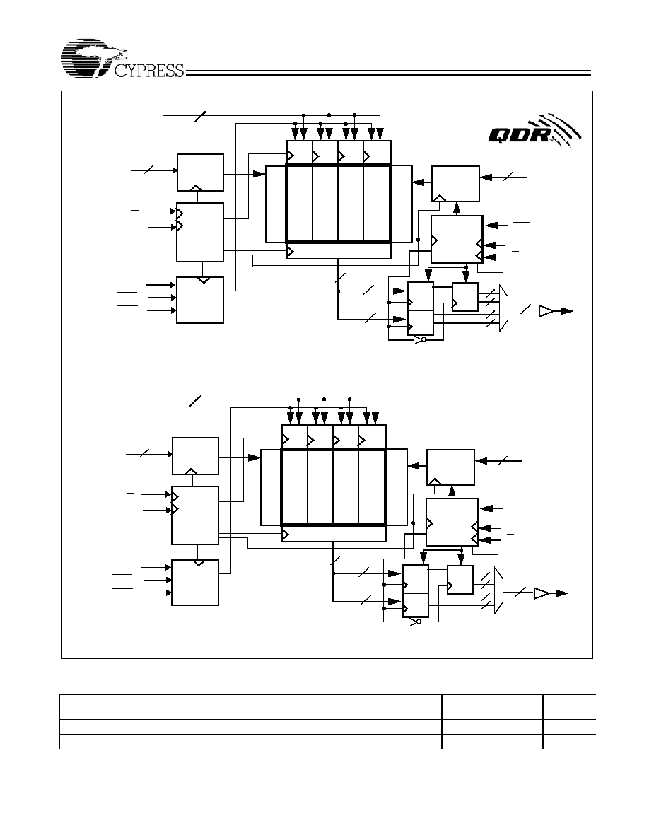
Logic Block Diagram (CY7C1305BV25)
256Kx1
8 Array
CLK
A
[17:0]
Gen.
K
K
Control
Logic
Address
Register
D
[17:0]
Re
a
d
Ad
d.
De
c
o
de
Read Data Reg.
RPS
WPS
Q
[17:0]
Control
Logic
Address
Register
Reg.
Reg.
Reg.
36
18
18
72
18
BWS
[0:1]
Vref
W
r
i
t
e A
d
d.
Deco
de
Write
Reg
36
A
(17:0)
18
C
C
256Kx1
8 Array
256Kx1
8 Array
256Kx1
8 Array
Write
Reg
Write
Reg
Write
Reg
18
Logic Block Diagram (CY7C1307BV25)
128
K x 3
6
Ar
ray
CLK
A
(16:0)
Gen.
K
K
Control
Logic
Address
Register
D
[35:0]
Re
a
d
Ad
d
.
D
e
c
o
de
Read Data Reg.
RPS
WPS
Q
[35:0]
Control
Logic
Address
Register
Reg.
Reg.
Reg.
72
17
36
144
36
BWS
[0:3]
Vref
W
r
i
t
e Ad
d. D
eco
de
Write
Reg
72
A
(16:0)
17
C
C
128
K x 3
6
Ar
ray
128
K x 3
6
Ar
ray
128
K x 3
6
Ar
ray
Write
Reg
Write
Reg
Write
Reg
36
PRELIMINARY
CY7C1305BV25
CY7C1307BV25
Document #: 38-05630 Rev. **
Page 3 of 21
\
Pin ConfigurationCY7C1305BV25 (Top View)
1
2
3
4
5
6
7
8
9
10
11
A
NC
GND/
144M
NC/ 36M
WPS
BWS
1
K
NC
RPS
A
GND/
72M
NC
B
NC
Q9
D9
A
NC
K
BWS
0
A
NC
NC
Q8
C
NC
NC
D10
VSS
A
NC
A
VSS
NC
Q7
D8
D
NC
D11
Q10
VSS
VSS
VSS
VSS
VSS
NC
NC
D7
E
NC
NC
Q11
VDDQ
VSS
VSS
VSS
VDDQ
NC
D6
Q6
F
NC
Q12
D12
VDDQ
VDD
VSS
VDD
VDDQ
NC
NC
Q5
G
NC
D13
Q13
VDDQ
VDD
VSS
VDD
VDDQ
NC
NC
D5
H
NC
VREF
VDDQ
VDDQ
VDD
VSS
VDD
VDDQ
VDDQ
VREF
ZQ
J
NC
NC
D14
VDDQ
VDD
VSS
VDD
VDDQ
NC
Q4
D4
K
NC
NC
Q14
VDDQ
VDD
VSS
VDD
VDDQ
NC
D3
Q3
L
NC
Q15
D15
VDDQ
VSS
VSS
VSS
VDDQ
NC
NC
Q2
M
NC
NC
D16
VSS
VSS
VSS
VSS
VSS
NC
Q1
D2
N
NC
D17
Q16
VSS
A
A
A
VSS
NC
NC
D1
P
NC
NC
Q17
A
A
C
A
A
NC
D0
Q0
R
TDO
TCK
A
A
A
C
A
A
A
TMS
TDI
Pin ConfigurationCY7C1307BV25 (Top View)
1
2
3
4
5
6
7
8
9
10
11
A
NC
GND/
288M
NC/ 72M
WPS
BWS
2
K
BWS
1
RPS
NC/
36M
GND/
144M
NC
B
Q27
Q18
D18
A
BWS
3
K
BWS
0
A
D17
Q17
Q8
C
D27
Q28
D19
VSS
A
NC
A
VSS
D16
Q7
D8
D
D28
D20
Q19
VSS
VSS
VSS
VSS
VSS
Q16
D15
D7
E
Q29
D29
Q20
VDDQ
VSS
VSS
VSS
VDDQ
Q15
D6
Q6
F
Q30
Q21
D21
VDDQ
VDD
VSS
VDD
VDDQ
D14
Q14
Q5
G
D30
D22
Q22
VDDQ
VDD
VSS
VDD
VDDQ
Q13
D13
D5
H
NC
VREF
VDDQ
VDDQ
VDD
VSS
VDD
VDDQ
VDDQ
VREF
ZQ
J
D31
Q31
D23
VDDQ
VDD
VSS
VDD
VDDQ
D12
Q4
D4
K
Q32
D32
Q23
VDDQ
VDD
VSS
VDD
VDDQ
Q12
D3
Q3
L
Q33
Q24
D24
VDDQ
VSS
VSS
VSS
VDDQ
D11
Q11
Q2
M
D33
Q34
D25
VSS
VSS
VSS
VSS
VSS
D10
Q1
D2
N
D34
D26
Q25
VSS
A
A
A
VSS
Q10
D9
D1
P
Q35
D35
Q26
A
A
C
A
A
Q9
D0
Q0
R
TDO
TCK
A
A
A
C
A
A
A
TMS
TDI
PRELIMINARY
CY7C1305BV25
CY7C1307BV25
Document #: 38-05630 Rev. **
Page 4 of 21
Pin Definitions
Name
I/O
Description
D
[x:0]
Input-
Synchronous
Data input signals, sampled on the rising edge of K and K clocks during valid write
operations.
CY7C1305BV25 D
[17:0]
CY7C1307BV25 D
[35:0]
WPS
Input-
Synchronous
Write Port Select, active LOW. Sampled on the rising edge of the K clock. When
asserted active, a Write operation is initiated. Deasserting will deselect the Write port.
Deselecting the Write port will cause D
[x:0]
to be ignored.
BWS
0
, BWS
1
,
BWS
2
, BWS
3
Input-
Synchronous
Byte Write Select 0, 1, 2, and 3active LOW. Sampled on the rising edge of the K and
K clocks during Write operations. Used to select which byte is written into the device
during the current portion of the Write operations. Bytes not written remain unaltered.
CY7C1305BV25 - BWS
0
controls D
[8:0]
and BWS
1
controls D
[17:9].
CY7C1307BV25 - BWS
0
controls D
[8:0]
, BWS
1
controls D
[17:9]
, BWS
2
controls D
[26:18]
and BWS
3
controls D
[35:27]
All the Byte Write Selects are sampled on the same edge as the data. Deselecting a
Byte Write Select will cause the corresponding byte of data to be ignored and not written
into the device.
A
Input-
Synchronous
Address Inputs. Sampled on the rising edge of the K clock during active Read and Write
operations. These address inputs are multiplexed for both Read and Write operations.
Internally, the device is organized as 1M x 18 (4 arrays each of 256K x 18) for
CY7C1305BV25 and 512K x 36 (4 arrays each of 128K x 36) for CY7C1307BV25.
Therefore, only 18 address inputs for CY7C1305BV25 and 17 address inputs for
CY7C1307BV25. These inputs are ignored when the appropriate port is deselected.
Q
[x:0]
Outputs-
Synchronous
Data Output signals. These pins drive out the requested data during a Read operation.
Valid data is driven out on the rising edge of both the C and C clocks during Read
operations or K and K when in single clock mode. When the Read port is deselected,
Q
[x:0]
are automatically three-stated.
CY7C1305BV25 - Q
[17:0]
CY7C1307BV25 - Q
[35:0]
RPS
Input-
Synchronous
Read Port Select, active LOW. Sampled on the rising edge of Positive Input Clock (K).
When active, a Read operation is initiated. Deasserting will cause the Read port to be
deselected. When deselected, the pending access is allowed to complete and the output
drivers are automatically three-stated following the next rising edge of the C clock. Each
read access consists of a burst of four sequential 18-bit or 36-bit transfers.
C
Input-Clock
Positive Output Clock Input. C is used in conjunction with C to clock out the Read data
from the device. C and C can be used together to deskew the flight times of various
devices on the board back to the controller. See application example for further details.
C
Input-Clock
Negative Output Clock Input. C is used in conjunction with C to clock out the Read
data from the device. C and C can be used together to deskew the flight times of various
devices on the board cack to the controller. See application example for further details.
K
Input-Clock
Positive Input Clock Input. The rising edge of K is used to capture synchronous inputs
to the device and to drive out data through Q
[x:0]
when in single clock mode. All accesses
are initiated on the rising edge of K.
K
Input-Clock
Negative Input Clock Input. K is used to capture synchronous inputs to the device and
to drive out data through Q
[x:0]
when in single clock mode.
ZQ
Input
Output Impedance Matching Input. This input is used to tune the device outputs to the
system data bus impedance. Q
[x:0]
output impedance are set to 0.2 x RQ, where RQ is
a resistor connected between ZQ and ground. Alternately, this pin can be connected
directly to V
DD
, which enables the minimum impedance mode. This pin cannot be
connected directly to VSS or left unconnected.
TDO
Output
TDO pin for JTAG
TCK
Input
TCK pin for JTAG
TDI
Input
TDI pin for JTAG
TMS
Input
TMS pin for JTAG
PRELIMINARY
CY7C1305BV25
CY7C1307BV25
Document #: 38-05630 Rev. **
Page 5 of 21
Introduction
Functional Overview
The CY7C1305BV25/CY7C1307BV25 are synchronous
pipelined Burst SRAMs equipped with both a Read port and a
Write port. The Read port is dedicated to Read operations and
the Write Port is dedicated to Write operations. Data flows into
the SRAM through the Write port and out through the Read
port. These devices multiplex the address inputs in order to
minimize the number of address pins required. By having
separate Read and Write ports, the device completely elimi-
nates the need to "turn-around" the data bus and avoids any
possible data contention, thereby simplifying system design.
Each access consists of four 18-bit data transfers in the case
of CY7C1305BV25 and four 36-bit data transfers in the case
of CY7C1307BV25, in two clock cycles.
Accesses for both ports are initiated on the rising edge of the
positive input clock (K). All synchronous input timing is refer-
enced from the rising edge of the input clocks (K and K) and
all output timing is referenced to the rising edge of output
clocks (C and C, or K and K when in single clock mode).
All synchronous data inputs (D
[x:0]
) pass through input
registers controlled by the rising edge of input clocks (K and
K). All synchronous data outputs (Q
[x:0]
) pass through output
registers controlled by the rising edge of the output clocks (C
and C, or K and K when in single clock mode).
All synchronous control (RPS, WPS, BWS
[0:x]
) inputs pass
through input registers controlled by the rising edge of input
clocks (K and K).
CY7C1305BV25 is described in the following sections. The
same basic descriptions apply to CY7C1307BV25.
Read Operations
The CY7C1305BV25 is organized internally as 4 arrays of
256K x 18. Accesses are completed in a burst of four
sequential 18-bit data words. Read operations are initiated by
asserting RPS
active at the rising edge of the Positive Input
Clock (K). The address presented to Address inputs are stored
in the Read address register. Following the next K clock rise
the corresponding lowest order 18-bit word of data is driven
onto the Q
[17:0]
using C as the output timing reference. On the
subsequent rising edge of C the next 18-bit data word is driven
onto the Q
[17:0]
. This process continues until all four 18-bit data
words have been driven out onto Q
[17:0]
. The requested data
will be valid 2.5 ns from the rising edge of the output clock
(C and C, or K and K when in single clock mode, 167-MHz
device). In order to maintain the internal logic, each Read
access must be allowed to complete. Each Read access
consists of four 18-bit data words and takes 2 clock cycles to
complete. Therefore, Read accesses to the device can not be
initiated on two consecutive K clock rises. The internal logic of
the device will ignore the second Read request. Read
accesses can be initiated on every other K clock rise. Doing
so will pipeline the data flow such that data is transferred out
of the device on every rising edge of the output clocks (C and
C, or K and K when in single clock mode).
When the read port is deselected, the CY7C1305BV25 will first
complete the pending read transactions. Synchronous internal
circuitry will automatically three-state the outputs following the
next rising edge of the positive output clock (C). This will allow
for a seamless transition between devices without the
insertion of wait states in a depth expanded memory.
Write Operations
Write operations are initiated by asserting WPS active at the
rising edge of the positive input clock (K). On the following K
clock rise the data presented to D
[17:0]
is latched and stored
into the lower 18-bit Write Data register provided BWS
[1:0]
are
both asserted active. On the subsequent rising edge of the
negative input clock (K) the information presented to D
[17:0]
is
also stored into the Write Data Register provided BWS
[1:0]
are
both asserted active. This process continues for one more
cycle until four 18-bit words (a total of 72 bits) of data are
stored in the SRAM. The 72 bits of data are then written into
the memory array at the specified location. Therefore, Write
accesses to the device can not be initiated on two consecutive
K clock rises. The internal logic of the device will ignore the
second Write request. Write accesses can be initiated on
every other rising edge of the positive clock (K). Doing so will
pipeline the data flow such that 18-bits of data can be trans-
ferred into the device on every rising edge of the input clocks
(K and K).
NC/36M
N/A
Address expansion for 36M. This is not connected to the die. Can be connected to any
voltage level on CY7C1305BV25/CY7C1307BV25.
GND/72M
Input
Address expansion for 72M. This should be tied LOW on the CY7C1305BV25.
NC/72M
N/A
Address expansion for 72M. This can be connected to any voltage level on
CY7C1307BV25.
GND/144M
Input
Address expansion for 144M. This should be tied LOW on
CY7C1305BV25/CY7C1307BV25.
GND/288M
Input
Address expansion for 144M. This should be tied LOW on CY7C1307BV25.
V
REF
Input-
Reference
Reference Voltage Input. Static input used to set the reference level for HSTL inputs
and Outputs as well as AC measurement points.
V
DD
Power Supply
Power supply inputs to the core of the device
V
SS
Ground
Ground for the device
V
DDQ
Power Supply
Power supply inputs for the outputs of the device
NC
N/A
Not connected to the die. Can be tied to any voltage level.
Pin Definitions
(continued)
Name
I/O
Description