Preliminary
18 Mb Burst of 4 Pipelined SRAM with QDR Architecture
CY7C1305V25
CY7C1307V25
Cypress Semiconductor Corporation
∑
3901 North First Street
∑
San Jose
∑
CA 95134
∑
408-943-2600
Document #: 38-05099 Rev. *A
Revised December 11, 2002
1305V25
Features
∑ Separate Independent Read and Write Data Ports
-- Supports concurrent transactions
∑ 167 MHz Clock for High Bandwidth
-- 2.5 ns Clock-to-Valid access time
∑ 4-Word Burst for reducing the address bus frequency
∑ Double Data Rate (DDR) interfaces on both Read & Write
Ports (data transferred at 333 MHz) @167 MHz
∑ Two input clocks (K and K) for precise DDR timing
-- SRAM uses rising edges only
∑ Two output clocks (C and C) accounts for clock skew
and flight time mis-matches
∑ Single multiplexed address input bus latches address
inputs for both READ and WRITE ports
∑ Separate Port Selects for depth expansion
∑ Synchronous internally self-timed writes
∑ 2.5V core power supply with HSTL Inputs and Outputs
∑ 13x15 mm 1.0 mm pitch fBGA package, 165 ball
(11x15 matrix)
∑ Variable drive HSTL output buffers
∑ Expanded HSTL output voltage (1.4V≠1.9V)
∑ JTAG Interface
Configurations
CY7C1305V25 ≠ 1 Mb x 18
CY7C1307V25 ≠ 512K x 36
Functional Description
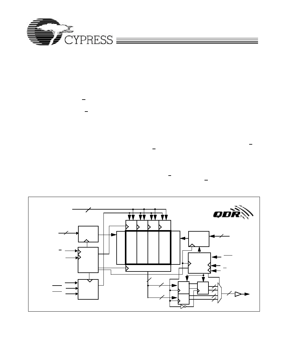
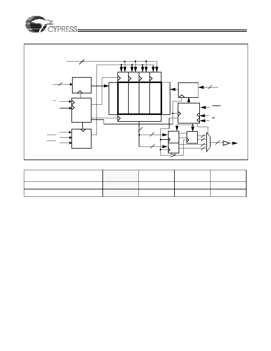
The CY7C1305V25/CY7C1307V25 are 2.5V Synchronous
Pipelined SRAMs equipped with QDR architecture. QDR ar-
chitecture consists of two separate ports to access the mem-
ory array. The Read port has dedicated Data Outputs to sup-
port Read operations and the Write Port has dedicated Data
Inputs to support Write operations. QDR architecture has sep-
arate data inputs and data outputs to completely eliminate the
need to "turn-around" the data bus required with common I/O
devices. Access to each port is accomplished through a com-
mon address bus. Addresses for Read and Write addresses
are latched on alternate rising edges of the input (K) clock.
Accesses to the device's Read and Write ports are completely
independent of one another. In order to maximize data
throughput, both Read and Write ports are equipped with Dou-
ble Data Rate (DDR) interfaces. Each address location is as-
sociated with four 18-bit words (CY7C1305V25) and four
36-bit words (CY7C1307V25) that burst sequentially into or
out of the device. Since data can be transferred into and out
of the device on every rising edge of both input clocks (K/K and
C/C) memory bandwidth is maximized while simplifying sys-
tem design by eliminating bus "turn-arounds."
Depth expansion is accomplished with Port Selects for each
port. Port selects allow each port to operate independently.
All synchronous inputs pass through input registers controlled
by the K or K input clocks. All data outputs pass through output
registers controlled by the C or C input clocks. Writes are con-
ducted with on-chip synchronous self-timed write circuitry.
Logic Block Diagram (CY7C1305V25)
256
Kx1
8
Arra
y
CLK
A
(17:0)
Gen.
K
K
Control
Logic
Address
Register
D
[17:0]
Read
A
d
d
.
Deco
d
e
Read Data Reg.
RPS
WPS
Q
[17:0]
Control
Logic
Address
Register
Reg.
Reg.
Reg.
36
18
18
72
18
BWS
[0:1]
Vref
W
r
i
t
e
Ad
d.
De
c
ode
Write
Reg
36
A
(17:0)
18
C
C
256
Kx1
8
Arra
y
256
Kx1
8
Arra
y
256
Kx1
8
Arra
y
Write
Reg
Write
Reg
Write
Reg
18
CY7C1305V25
CY7C1307V25
Preliminary
Document #: 38-05099 Rev. *A
Page 2 of 28
Selection Guide
[1]
7C1305V25-200
7C1307V25-200
7C1305V25-167
7C1307V25-167
7C1305V25-133
7C1307V25-133
7C1305V25-100
7C1307V25-100
Maximum Operating Frequency (MHz)
200
167
133
100
Maximum Operating Current (mA)
500
450
350
230
Note:
1.
Shaded areas contain advance information.
Logic Block Diagram (CY7C1307V25)
1
28K
x 3
6
Arra
y
CLK
A
(16:0)
Gen.
K
K
Control
Logic
Address
Register
D
[35:0]
R
e
ad Add
.
Dec
o
de
Read Data Reg.
RPS
WPS
Q
[35:0]
Control
Logic
Address
Register
Reg.
Reg.
Reg.
72
17
36
144
36
BWS
[0:3]
Vref
W
r
i
t
e A
d
d
.
Deco
d
e
Write
Reg
72
A
(16:0)
17
C
C
1
28K
x 3
6
Arra
y
1
28K
x 3
6
Arra
y
1
28K
x 3
6
Arra
y
Write
Reg
Write
Reg
Write
Reg
36
CY7C1305V25
CY7C1307V25
Preliminary
Document #: 38-05099 Rev. *A
Page 5 of 28
Pin Definitions
Name
I/O
Description
D
[x:0]
Input-
Synchronous
Data input signals, sampled on the rising edge of K and K clocks during valid write
operations.
CY7C1305V25 ≠ D
[17:0]
CY7C1307V25 ≠ D
[35:0]]
WPS
Input-
Synchronous
Write Port Select, active LOW. Sampled on the rising edge of the K clock. When as-
serted active, a write operation is initiated. Deasserting will deselect the Write port.
Deselecting the Write port will cause D
[x:0]
to be ignored.
BWS
0
, BWS
1
,
BWS
2
, BWS
3
Input-
Synchronous
Byte Write Select 0, 1, 2, and 3 - active LOW. Sampled on the rising edge of the K and
K clocks during write operations. Used to select which byte is written into the device
during the current portion of the write operations. Bytes not written remain unaltered.
CY7C1305V25 - BWS
0
controls D
[8:0]
and BWS
1
controls D
[17:9].
CY7C1307V25 - BWS
0
controls D
[8:0]
, BWS
1
controls D
[17:9]
, BWS
2
controls D
[26:18]
and BWS
3
controls D
[35:27]
All the byte writes are sampled on the same edge as the data. Deselecting a Byte Write
Select will cause the corresponding byte of data to be ignored and not written into the
device.
A
Input-
Synchronous
Address Inputs. Sampled on the rising edge of the K clock during active read and write
operations. These address inputs are multiplexed for both Read and Write operations.
Internally, the device is organized as 1 Mb x 18 (4 arrays each of 256K x 18) for
CY7C1305V25 and 256K x 36 (4 arrays each of 128K x 36) for CY7C1307V25. There-
fore, only 18 address inputs for CY7C1305V25 and 17 address inputs for
CY7C1307V25.These inputs are ignored when the appropriate port is deselected.
Q
[x:0]
Outputs-
Synchronous
Data Output signals. These pins drive out the requested data during a Read operation.
Valid data is driven out on the rising edge of both the C and C clocks during Read
operations or K and K. when in single clock mode. When the Read port is deselected,
Q
[x:0]
are automatically three-stated.
CY7C1305V25 - Q
[17:0]
CY7C1307V25 - Q
[35:0]
RPS
Input-
Synchronous
Read Port Select, active LOW. Sampled on the rising edge of positive input clock (K).
When active, a Read operation is initiated. Deasserting will cause the Read port to be
deselected. When deselected, the pending access is allowed to complete and the out-
put drivers are automatically three-stated following the next rising edge of the K clock.
Each read access consists of a burst of four sequential 18-bit or 36-bit transfers.
C
Input-Clock
Positive Output Clock, input. C is used in conjunction with C to clock out the Read data
from the device. C and C can be used together to deskew the flight times of various
devices on the board back to the controller. See application example for further details.
C
Input-Clock
Negative Output Clock, input. C is used in conjunction with C to clock out the Read data
from the device. C and C can be used together to deskew the flight times of various
devices on the board cack to the controller. See application example for further details.
K
Input-Clock
Positive Input Clock, input. The rising edge of K is used to capture synchronous inputs
to the device and to drive out data through Q
[x:0]
when in single clock mode. All accesses
are initiated on the rising edge of K.
K
Input-Clock
Negative Input Clock Input. K is used to capture synchronous inputs being presented
to the device and to drive out data through Q
[x:0]
when in single clock mode.
ZQ
Input
Output Impedance Matching Input. This input is used to tune the device outputs to the
system data bus impedance. Q
[x:0]
output impedance are set to 0.2 x RQ, where RQ is
a resistor connected between ZQ and ground. Alternately, this pin can be connected
directly to V
DD
, which enables the minimum impedance mode. This pin cannot be con-
nected directly to GND or left unconnected.