Äîêóìåíòàöèÿ è îïèñàíèÿ www.docs.chipfind.ru
PRELIMINARY
18-Mb QDRTM-II SRAM 2-Word Burst Architecture
CY7C1310AV18
CY7C1312AV18
CY7C1314AV18
Cypress Semiconductor Corporation
·
3901 North First Street
·
San Jose
,
CA 95134
·
408-943-2600
Document #: 38-05497 Rev. *A
Revised June 1, 2004
Features
· Separate independent Read and Write data ports
-- Supports concurrent transactions
· 167-MHz clock for high bandwidth
· 2-Word Burst on all accesses
· Double Data Rate (DDR) interfaces on both Read and
Write ports (data transferred at 333 MHz) @ 167MHz
· Two input clocks (K and K) for precise DDR timing
-- SRAM uses rising edges only
· Two output clocks (C and C) account for clock skew
and flight time mismatching
· Echo clocks (CQ and CQ) simplify data capture in high
speed systems
· Single multiplexed address input bus latches address
inputs for both Read and Write ports
· Separate Port Selects for depth expansion
· Synchronous internally self-timed writes
· Available in x8, x18, and x36 configurations
· Full data coherancy , providing most current data
· Core Vdd=1.8V(+/-0.1V);I/O Vddq=1.4V to Vdd
· 13 x 15 x 1.4 mm 1.0-mm pitch FBGA package, 165 ball
(11x15 matrix)
· Variable drive HSTL output buffers
· JTAG 1149.1 compatible test access port
· Delay Lock Loop (DLL) for accurate data placement
Configurations
CY7C1310AV18 2M x 8
CY7C1312AV18 1M x 18
CY7C1314AV18 512K x 36
Functional Description
The CY7C1310AV18/CY7C1312AV18/CY7C1314AV18 are
1.8V Synchronous Pipelined SRAMs, equipped with QDR-II
architecture. QDR-II architecture consists of two separate
ports to access the memory array. The Read port has
dedicated Data Outputs to support Read operations and the
Write Port has dedicated Data Inputs to support Write opera-
tions. QDR-II architecture has separate data inputs and data
outputs to completely eliminate the need to "turn-around" the
data bus required with common I/O devices. Access to each
port is accomplished through a common address bus. The
Read address is latched on the rising edge of the K clock and
the Write address is latched on the rising edge of the K clock.
Accesses to the QDR-II Read and Write ports are completely
independent of one another. In order to maximize data
throughput, both Read and Write ports are equipped with
Double Data Rate (DDR) interfaces. Each address location is
associated with two 8-bit words (CY7C1310AV18) or 18-bit
words (CY7C1312AV18) or 36-bit words (CY7C1314AV18)
that burst sequentially into or out of the device. Since data can
be transferred into and out of the device on every rising edge
of both input clocks (K and K and C and C), memory bandwidth
is maximized while simplifying system design by eliminating
bus "turn-arounds."
Depth expansion is accomplished with Port Selects for each
port. Port selects allow each port to operate independently.
All synchronous inputs pass through input registers controlled
by the K or K input clocks. All data outputs pass through output
registers controlled by the C or C (or K or K in a single clock
domain) input clocks. Writes are conducted with on-chip
synchronous self-timed write circuitry.
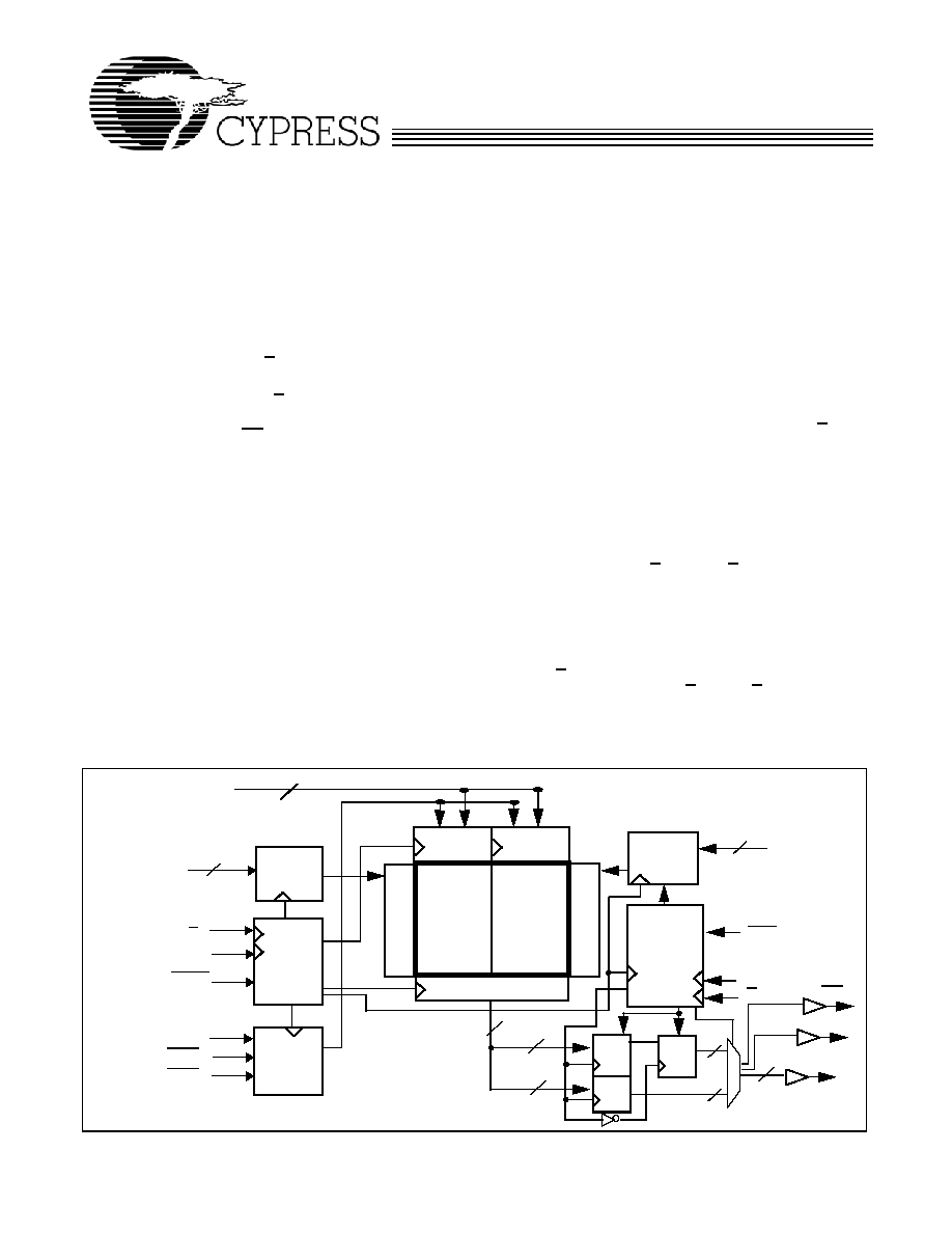
Logic Block Diagram (CY7C1310AV18)
CLK
A
(19:0)
Gen.
K
K
Control
Logic
Address
Register
D
[7:0]
Rea
d
A
dd.
De
co
de
Read Data Reg.
RPS
WPS
Q
[7:0]
Control
Logic
Address
Register
Reg.
Reg.
Reg.
8
20
8
16
8
BWS
[1:0]
V
REF
W
r
i
t
e Ad
d.
Dec
ode
8
A
(19:0)
20
C
C
8
1M x 8 Ar
r
a
y
1M
x 8 Ar
r
a
y
Write
Reg
Write
Reg
CQ
CQ
8
DOFF
CY7C1310AV18
CY7C1312AV18
CY7C1314AV18
PRELIMINARY
Document #: 38-05497 Rev. *A
Page 2 of 21
Selection Guide
167 MHz
133 MHz
Unit
Maximum Operating Frequency
167
133
MHz
Maximum Operating Current
800
700
mA
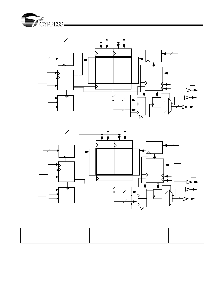
Logic Block Diagram (CY7C1312AV18)
CLK
A
(18:0)
Gen.
K
K
Control
Logic
Address
Register
D
[17:0]
Read
A
dd.
De
cod
e
Read Data Reg.
RPS
WPS
Q
[17:0]
Control
Logic
Address
Register
Reg.
Reg.
Reg.
18
19
18
36
18
BWS
[1:0]
V
REF
W
r
i
t
e Add
.
Dec
ode
18
A
(18:0)
19
C
C
18
51
2K x
18
Ar
r
a
y
512
K
x 18 Ar
r
a
y
Write
Reg
Write
Reg
CQ
CQ
18
DOFF
Logic Block Diagram (CY7C1314AV18)
CLK
A
(17:0)
Gen.
K
K
Control
Logic
Address
Register
D
[35:0]
R
e
ad
A
d
d.
De
c
o
d
e
Read Data Reg.
RPS
WPS
Q
[35:0]
Control
Logic
Address
Register
Reg.
Reg.
Reg.
36
18
36
72
36
BWS
[3:0]
V
REF
W
r
ite Ad
d
.
D
e
c
o
de
36
A
(17:0)
18
C
C
36
256K x
3
6
Arr
a
y
2
56K x
3
6
Arr
a
y
Write
Reg
Write
Reg
CQ
CQ
36
DOFF
CY7C1310AV18
CY7C1312AV18
CY7C1314AV18
PRELIMINARY
Document #: 38-05497 Rev. *A
Page 3 of 21
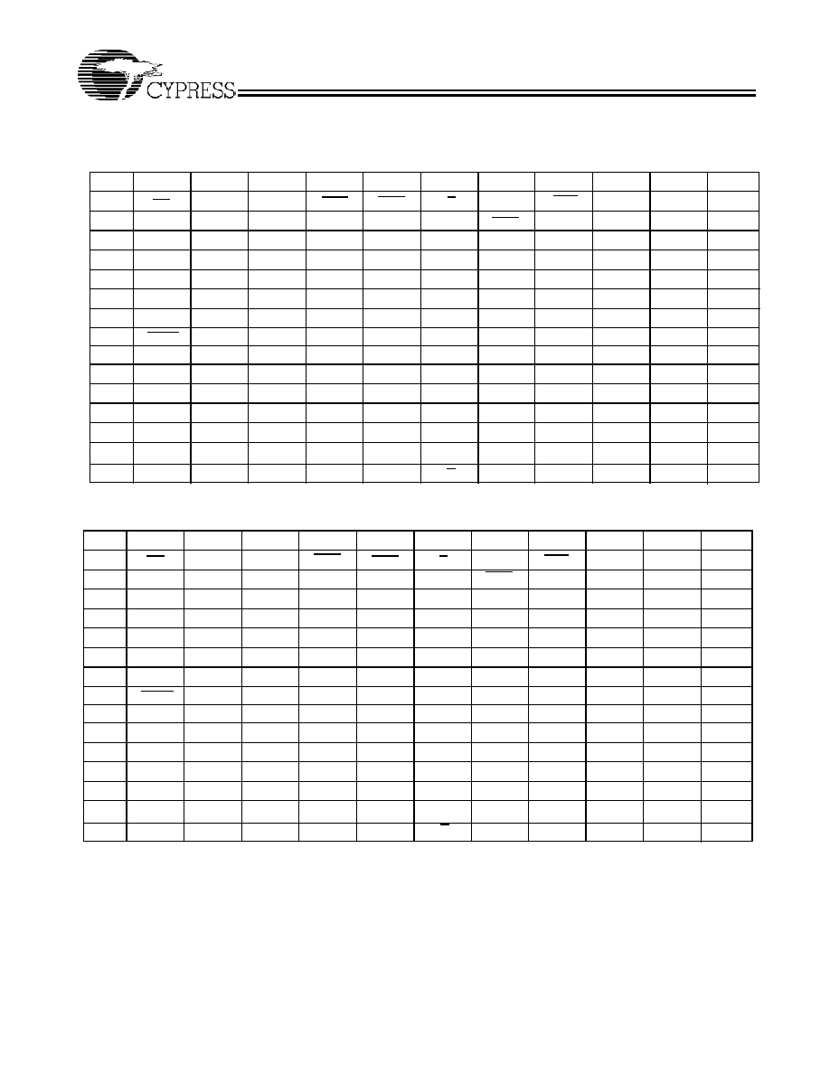
Pin Configurations
CY7C1310AV18 (2M × 8) 11 × 15 BGA
2
3
4
5
6
7
1
A
B
C
D
E
F
G
H
J
K
L
M
N
P
R
A
CQ
NC
NC
NC
NC
DOFF
NC
V
SS
/72M
A
BWS
1
K
WPS
NC/144M
NC
NC
NC
NC
NC
TDO
NC
NC
D5
NC
NC
NC
TCK
NC
NC
A NC/288M
K
BWS
0
V
SS
A
A
A
NC
V
SS
V
SS
V
SS
VSS
V
DD
A
V
SS
V
SS
V
SS
V
DD
Q4
NC
V
DDQ
NC
NC
NC
NC
Q7
A
V
DDQ
V
SS
V
DDQ
V
DD
V
DD
Q5
V
DDQ
V
DD
V
DDQ
V
DD
V
DDQ
V
DD
V
SS
V
DD
V
DDQ
V
DDQ
V
SS
V
SS
V
SS
V
SS
A
A
C
V
SS
A
A
A
D4
V
SS
NC
V
SS
NC
NC
V
REF
V
SS
V
DD
V
SS
V
SS
A
V
SS
C
NC
Q6
NC
D7
D6
V
DD
A
8
9
10
11
NC
A
V
SS
/36M
RPS
CQ
A NC
NC
Q3
V
SS
NC
NC
D3
NC
V
SS
NC
Q2
NC
NC
NC
V
REF
NC
NC
V
DDQ
NC
V
DDQ
NC
NC
V
DDQ
V
DDQ
V
DDQ
D1
V
DDQ
NC
Q1
NC
V
DDQ
V
DDQ
NC
V
SS
NC
D0
NC
TDI
TMS
V
SS
A
NC
A
NC
D2
NC
ZQ
NC
Q0
NC
NC
NC
NC
A
CY7C1312AV18 (1M × 18) 11 × 15 BGA
2
3
4
5
6
7
1
A
B
C
D
E
F
G
H
J
K
L
M
N
P
R
A
CQ
NC
NC
NC
NC
DOFF
NC
V
SS
/144M NC/36M
BWS
1
K
WPS
NC/288M
Q9
D9
NC
NC
NC
TDO
NC
NC
D13
NC
NC
NC
TCK
NC
D10
A NC
K
BWS
0
V
SS
A
A
A
Q10
V
SS
V
SS
V
SS
V
SS
V
DD
A
V
SS
V
SS
V
SS
V
DD
Q11
D12
V
DDQ
D14
Q14
D16
Q16
Q17
A
V
DDQ
V
SS
V
DDQ
V
DD
V
DD
Q13
V
DDQ
V
DD
V
DDQ
V
DD
V
DDQ
V
DD
V
SS
V
DD
V
DDQ
V
DDQ
V
SS
V
SS
V
SS
V
SS
A
A
C
V
SS
A
A
A
D11
V
SS
NC
V
SS
Q12
NC
V
REF
V
SS
V
DD
V
SS
V
SS
A
V
SS
C
NC
Q15
NC
D17
D15
V
DD
A
8
9
10
11
Q0
A
V
SS
/72M
RPS
CQ
A NC
NC
Q8
V
SS
NC
Q7
D8
NC
V
SS
NC
Q6
D5
NC
NC
V
REF
NC
Q3
V
DDQ
NC
V
DDQ
NC
Q5
V
DDQ
V
DDQ
V
DDQ
D4
V
DDQ
NC
Q4
NC
V
DDQ
V
DDQ
NC
V
SS
NC
D2
NC
TDI
TMS
V
SS
A
NC
A
D7
D6
NC
ZQ
D3
Q2
D1
Q1
D0
NC
A
CY7C1310AV18
CY7C1312AV18
CY7C1314AV18
PRELIMINARY
Document #: 38-05497 Rev. *A
Page 4 of 21
Pin Definitions
Pin Name
I/O
Pin Description
D
[x:0]
Input-
Synchronous
Data input signals, sampled on the rising edge of K and K clocks during valid write
operations.
CY7C1310AV18 - D
[7:0]
CY7C1312AV18 - D
[17:0]
CY7C1314AV18 - D
[35:0]
WPS
Input-
Synchronous
Write Port Select, active LOW. Sampled on the rising edge of the K clock. When
asserted active, a write operation is initiated. Deasserting will deselect the Write port.
Deselecting the Write port will cause D
[x:0]
to be ignored.
BWS
0
, BWS
1
,
BWS
2
, BWS
3
Input-
Synchronous
Byte Write Select 0, 1, 2 and 3
- active LOW. Sampled on the rising edge of the K and
K clocks during write operations. Used to select which byte is written into the device
during the current portion of the write operations. Bytes not written remain unaltered.
CY7C1310AV18
- BWS
0
controls D
[3:0]
and BWS
1
controls D
[7:4]
.
CY7C1312AV18
- BWS
0
controls D
[8:0]
and BWS
1
controls D
[17:9].
CY7C1314AV18
- BWS
0
controls D
[8:0]
, BWS
1
controls D
[17:9]
, BWS
2
controls D
[26:18]
and BWS
3
controls D
[35:27].
All the Byte Write Selects are sampled on the same edge as the data. Deselecting a Byte
Write Select will cause the corresponding byte of data to be ignored and not written into
the device.
A
Input-
Synchronous
Address Inputs. Sampled on the rising edge of the K (read address) and K (write
address) clocks during active read and write operations. These address inputs are multi-
plexed for both Read and Write operations. Internally, the device is organized as 2M x 8
(2 arrays each of 1M x 8) for CY7C1310AV18, 1M x 18 (2 arrays each of 512K x 18) for
CY7C1312AV18 and 512K x 36 (2 arrays each of 256K x 36) for CY7C1314AV18.
Therefore, only 20 address inputs are needed to access the entire memory array of
CY7C1310AV18, 19 address inputs for CY7C1312AV18 and 18 address inputs for
CY7C1314AV18. These inputs are ignored when the appropriate port is deselected.
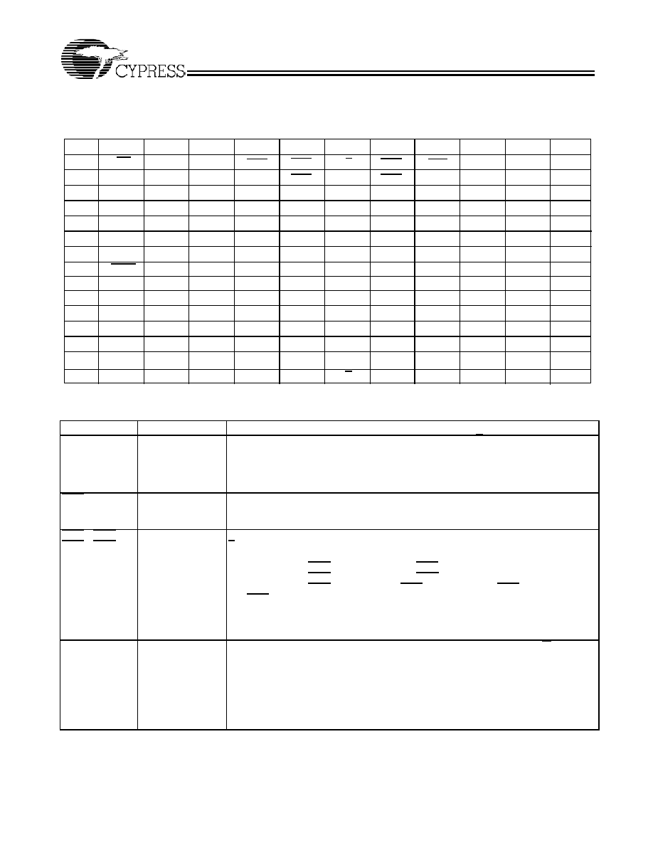
Pin Configurations
(continued)
2
3
4
5
6
7
1
A
B
C
D
E
F
G
H
J
K
L
M
N
P
R
A
CQ
Q27
D27
D28
D34
DOFF
Q33
V
SS
/288M NC/72M
BWS
2
K
WPS
BWS
1
Q18
D18
Q30
D31
D33
TDO
Q28
D29
D22
D32
Q34
Q31
TCK
D35
D19
A
BWS
3
K
BWS
0
V
SS
A
A
A
Q19
V
SS
V
SS
V
SS
V
SS
V
DD
A
V
SS
V
SS
V
SS
V
DD
Q20
D21
V
DDQ
D23
Q23
D25
Q25
Q26
A
V
DDQ
V
SS
V
DDQ
V
DD
V
DD
Q22
V
DDQ
V
DD
V
DDQ
V
DD
V
DDQ
V
DD
V
SS
V
DD
V
DDQ
V
DDQ
V
SS
V
SS
V
SS
V
SS
A
A
C
V
SS
A
A
A
D20
V
SS
Q29
V
SS
Q21
D30
V
REF
V
SS
V
DD
V
SS
V
SS
A
V
SS
C
Q32
Q24
Q35
D26
D24
V
DD
A
8
9
10
11
Q0
NC/36M V
SS
/144M
RPS
CQ
A D17
Q17
Q8
V
SS
D16
Q7
D8
Q16
V
SS
D15
Q6
D5
D9
Q14
V
REF
Q11
Q3
V
DDQ
Q15
V
DDQ
D14
Q5
V
DDQ
VDDQ
V
DDQ
D4
V
DDQ
D12
Q4
Q12
V
DDQ
V
DDQ
D11
V
SS
D10
D2
Q10
TDI
TMS
V
SS
A
Q9
A
D7
D6
D13
ZQ
D3
Q2
D1
Q1
D0
Q13
A
CY7C1314AV18 (512k × 36) 11 × 15 BGA
CY7C1310AV18
CY7C1312AV18
CY7C1314AV18
PRELIMINARY
Document #: 38-05497 Rev. *A
Page 5 of 21
Q
[x:0]
Outputs-
Synchronous
Data Output signals. These pins drive out the requested data during a Read operation.
Valid data is driven out on the rising edge of both the C and C clocks during Read
operations or K and K when in single clock mode. When the Read port is deselected,
Q
[x:0]
are automatically tri-stated.
CY7C1310AV18
- Q
[7:0]
CY7C1312AV18
- Q
[17:0]
CY7C1314AV18
- Q
[35:0]
RPS
Input-
Synchronous
Read Port Select, active LOW. Sampled on the rising edge of Positive Input Clock (K).
When active, a Read operation is initiated. Deasserting will cause the Read port to be
deselected. When deselected, the pending access is allowed to complete and the output
drivers are automatically tri-stated following the next rising edge of the C clock. Each
read access consists of a burst of two sequential transfers.
C
Input-Clock
Positive Output Clock Input. C is used in conjunction with C to clock out the Read data
from the device. C and C can be used together to deskew the flight times of various
devices on the board back to the controller. See application example for further details.
C
Input-Clock
Negative Output Clock Input. C is used in conjunction with C to clock out the Read data
from the device. C and C can be used together to deskew the flight times of various
devices on the board back to the controller. See application example for further details.
K
Input-Clock
Positive Input Clock Input. The rising edge of K is used to capture synchronous inputs
to the device and to drive out data through Q
[x:0]
when in single clock mode. All accesses
are initiated on the rising edge of K.
K
Input-Clock
Negative Input Clock Input. K is used to capture synchronous inputs being presented
to the device and to drive out data through Q
[x:0]
when in single clock mode.
CQ
Echo Clock
CQ is referenced with respect to C. This is a free running clock and is synchronized
to the output clock(C) of the QDR-II. In the single clock mode, CQ is generated with
respect to K. The timings for the echo clocks are shown in the AC timing table.
CQ
Echo Clock
CQ is referenced with respect to C. This is a free running clock and is synchronized
to the output clock(C) of the QDR-II. In the single clock mode, CQ is generated with
respect to K. The timings for the echo clocks are shown in the AC timing table.
ZQ
Input
Output Impedance Matching Input. This input is used to tune the device outputs to the
system data bus impedance. CQ,CQ and Q
[x:0]
output impedance are set to 0.2 x RQ,
where RQ is a resistor connected between ZQ and ground. Alternately, this pin can be
connected directly to V
DD
, which enables the minimum impedance mode. This pin cannot
be connected directly to GND or left unconnected.
DOFF
Input
DLL Turn Off Active LOW. Connecting this pin to ground will turn off the DLL inside
the device. The timings in the DLL turned off operation will be different from those listed
in this data sheet. More details on this operation can be found in the application note,
"DLL Operation in the QDR-II."
TDO
Output
TDO for JTAG.
TCK
Input
TCK pin for JTAG.
TDI
Input
TDI pin for JTAG.
TMS
Input
TMS pin for JTAG.
NC
N/A
Not connected to the die. Can be tied to any voltage level.
NC/36M
N/A
Address expansion for 36M. This is not connected to the die and so can be tied to any
voltage level.
NC/72M
N/A
Address expansion for 72M. This is not connected to the die and so can be tied to any
voltage level.
V
SS
/72M
Input
Address expansion for 72M. This must be tied LOW on the 18M devices.
V
SS
/144M
Input
Address expansion for 144M. This must be tied LOW on the 18M devices.
V
SS/
288M
Input
Address expansion for 288M. This must be tied LOW on the 18M devices.
Pin Definitions
(continued)
Pin Name
I/O
Pin Description