ADVANCE INFORMATION
18-Mb 2-Word Burst SRAM with DDR-I Architecture
CY7C1397V25
CY7C1322V25
Cypress Semiconductor Corporation
∑
3901 North First Street
∑
San Jose
∑
CA 95134
∑
408-943-2600
Document #: 38-05175 Rev. **
Revised October 26, 2001
397V25
Features
∑ 18-Mb Density (1M x 18, 512K x 36)
-- Supports concurrent transactions
∑ 300-MHz Clock for High Bandwidth
∑ 2-Word Burst for reducing address bus frequency
∑ Double Data Rate (DDR) interfaces (data transferred at
600 MHz) @300 MHz
∑ Two input clocks (K and K) for precise DDR timing
-- SRAM uses rising edges only
∑ Two output clocks (C and C) accounts for clock skew
and flight time mismatches
∑ Separate Port Selects for depth expansion
∑ Synchronous internally self-timed writes
∑ 2.5V core power supply with HSTL Inputs and Outputs
∑ Variable drive HSTL output buffers
∑ Expanded HSTL output voltage (1.4V≠V
DD
)
∑ 13x15 mm 1.0-mm pitch fBGA package, 165 ball (11x15
matrix)
∑ JTAG Interface
Configurations
CY7C1397V25 ≠ 1M x 18
CY7C1322V25 ≠ 512K x 36
Functional Description
The CY7C1397V25/CY7C1322V25 are 2.5V Synchronous
Pipelined SRAMs equipped with DDR-I (Double Data Rate)
architecture. The DDR-I consists of an SRAM core with ad-
vanced synchronous peripheral circuitry and a 1-bit burst
counter. Addresses for Read and Write are latched on alter-
nate rising edges of the input (K) clock. Write data is registered
on the rising edges of both K and K. Read data is driven on the
rising edges of C and C if provided, or on the rising edge of K
and K if C/C are not provided. Every read or write operation is
associated with two words that burst sequentially into or out of
the device. The burst counter takes in the least significant bit
of the external address and bursts two 18-bit words in the case
of CY7C1397V25 and two 36-bit words in the case of
CY7C1322V25. Depth expansion is accomplished with Port
Selects for each port. Port selects allow each port to operate
independently.
Asynchronous inputs include impedance match (ZQ). Syn-
chronous data outputs (Q, sharing the same physical pins as
the data inputs D) are tightly matched to the two output echo
clocks CQ/CQ, eliminating the need for separately capturing
data from each individual DDR SRAM in the system design.
Output data clocks (C/C) are also provided for maximum sys-
tem clocking and data synchronization flexibility.
All synchronous inputs pass through input registers controlled
by the K or K input clocks. All data outputs pass through output
registers controlled by the C or C input clocks. Writes are con-
ducted with on-chip synchronous self-timed write circuitry.
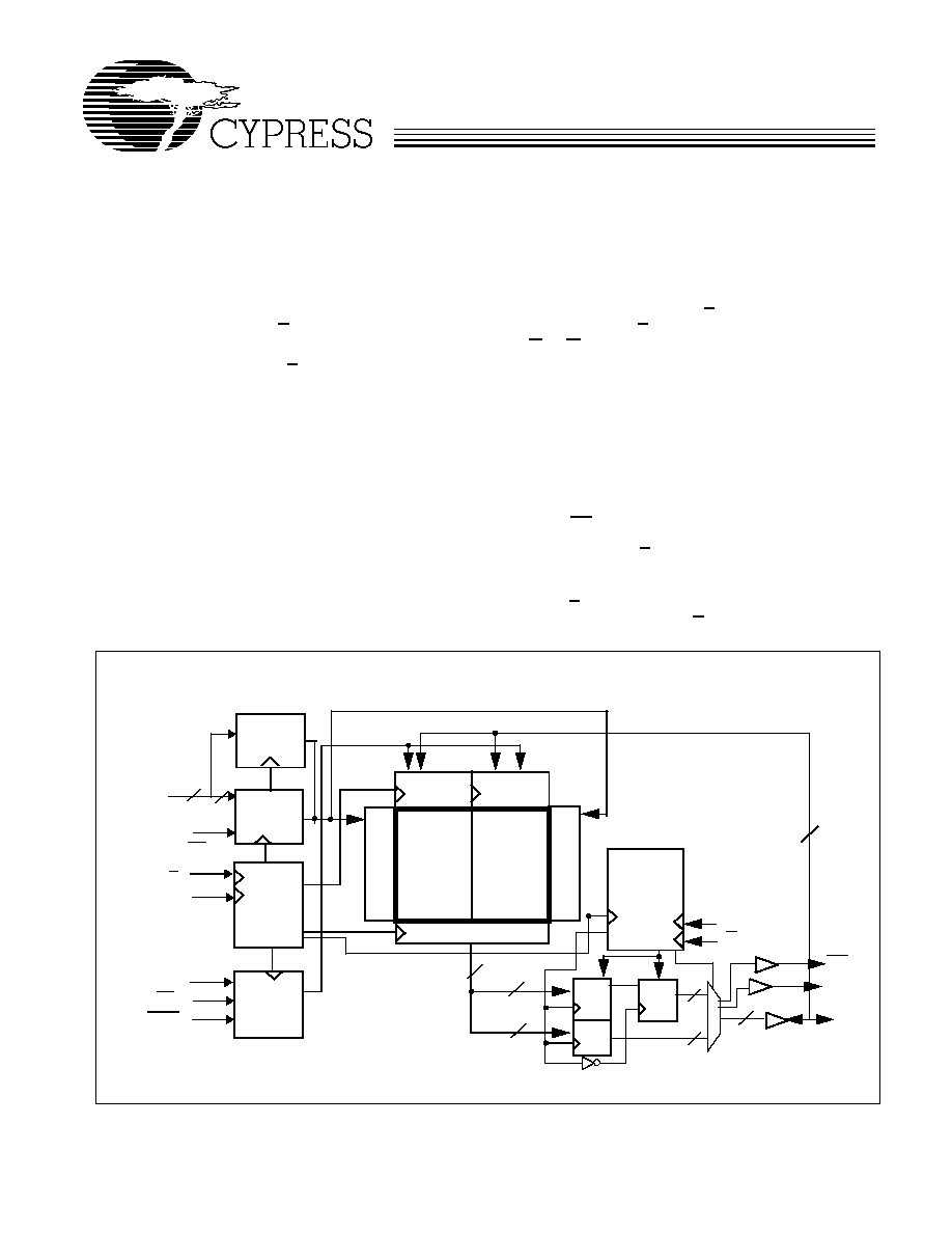
Logic Block Diagram (CY7C1397V25)
CLK
A
(19:0)
Gen.
K
K
Control
Logic
Address
Register
R
e
ad Add.
D
e
c
o
de
Read Data Reg.
R/W
DQ
[17:0]
Output
Logic
Reg.
Reg.
Reg.
18
18
36
18
BWS
[1:0]
V
REF7
W
r
it
e Add
.
D
e
c
o
de
18
20
C
C
18
LD
Control
Burst
Logic
A
(1:0)
A
(19:2)
18
5
12K
x 1
8
Arra
y
51
2K x
1
8
Arra
y
Write
Reg
Write
Reg
CQ
CQ
CY7C1397V25
CY7C1322V25
ADVANCE INFORMATION
Document #: 38-05175 Rev. **
Page 2 of 26
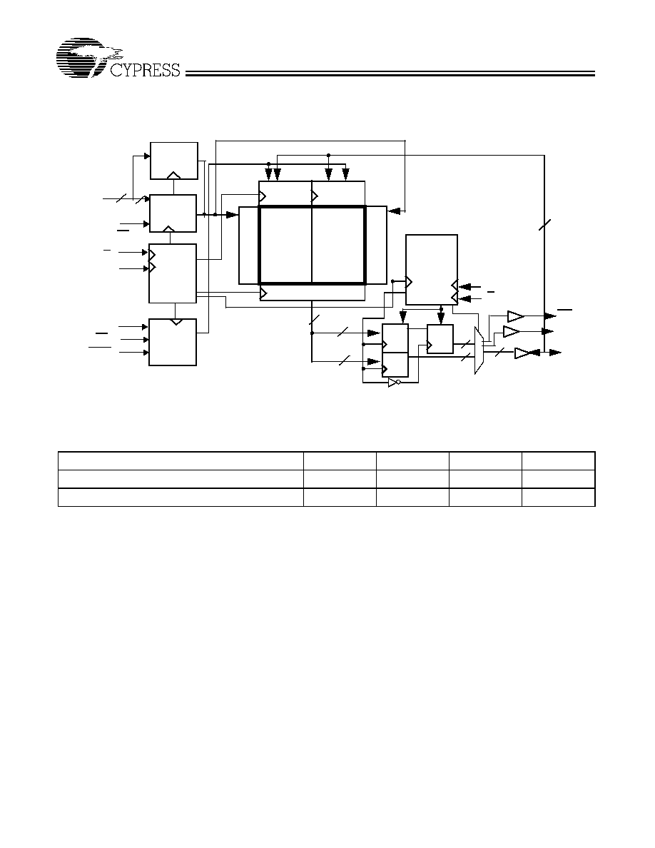
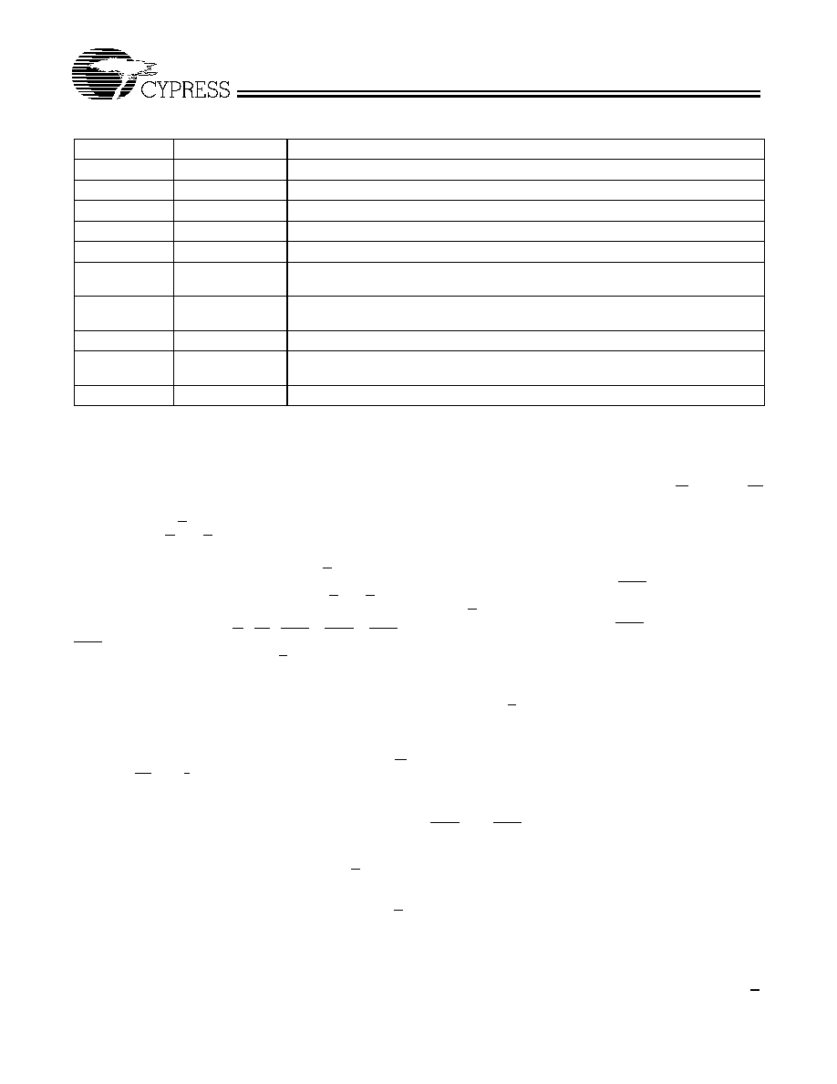
Selection Guide
300 MHz
250 MHz
200 MHz
167 MHz
Maximum Operating Frequency (MHz)
300
250
200
167
Maximum Operating Current (mA)
TBD
TBD
TBD
TBD
Logic Block Diagram (CY7C1322V25)
CLK
A
(18:0)
Gen.
K
K
Control
Logic
Address
Register
R
e
ad
A
d
d.
D
e
c
ode
Read Data Reg.
R/W
DQ
[35:0]
Output
Logic
Reg.
Reg.
Reg.
36
72
36
BWS
[3:0]
V
REF
W
r
it
e Add.
D
e
c
o
de
36
19
C
C
36
LD
Control
Burst
Logic
A
(1:0)
A
(18:2)
17
25
6K x
36
Array
256
K x
36 Ar
ray
Write
Reg
Write
Reg
CQ
CQ
36
36
CY7C1397V25
CY7C1322V25
ADVANCE INFORMATION
Document #: 38-05175 Rev. **
Page 3 of 26
Pin Configurations
CY7C1397V25 (1M x 18) - 11 x 15 FBGA
2
3
4
5
6
7
1
A
B
C
D
E
F
G
H
J
K
L
M
N
P
R
A
CQ
NC
NC
NC
NC
NC
NC
GND/72M
A
BWS
1
K
WE
NC
DQ9
NC
NC
NC
NC
TDO
NC
NC
NC
NC
NC
NC
TCK
NC
NC
A NC
K
BWS
0
VSS
A
A0
A
DQ10
VSS
VSS
VSS
VSS
VDD
A
VSS
VSS
VSS
VDD
DQ11
NC
VDDQ
NC
DQ14
NC
DQ16
DQ17
A
VDDQ
VSS
VDDQ
VDD
VDD
DQ13
VDDQ
VDD
VDDQ
VDD
VDDQ
VDD
VSS
VDD
VDDQ
VDDQ
VSS
VSS
VSS
VSS
A
A
C
VSS
A
A
A
NC
VSS
NC
VSS
DQ12
NC
VREF
VSS
VDD
VSS
VSS
A
VSS
C
NC
DQ15
NC
NC
NC
VDD
A
8
9
10
11
DQ0
A
GND/36M
LD
CQ
A NC
NC
DQ8
VSS
NC
DQ7
NC
NC
VSS
NC
DQ6
NC
NC
NC
VREF
NC
DQ3
VDDQ
NC
VDDQ
NC
DQ5
VDDQ
VDDQ
VDDQ
NC
VDDQ
NC
DQ4
NC
VDDQ
VDDQ
NC
VSS
NC
NC
NC
TDI
TMS
VSS
A
NC
A
NC
NC
NC
ZQ
NC
DQ2
NC
DQ1
NC
NC
A
CY7C1322V25 (512K x 36) - 11 x 15 FBGA
2
3
4
5
6
7
1
A
B
C
D
E
F
G
H
J
K
L
M
N
P
R
A
CQ
NC
NC
NC
NC
NC
NC
GND/144M NC/36M
BWS
2
K
WE
BWS
1
DQ27
DQ18
NC
NC
NC
TDO
NC
NC
DQ31
NC
NC
NC
TCK
NC
DQ28
A BWS
3
K
BWS
0
VSS
A
A0
A
DQ19
VSS
VSS
VSS
VSS
VDD
A
VSS
VSS
VSS
VDD
DQ20
DQ21
VDDQ
DQ32
DQ23
DQ34
DQ25
DQ26
A
VDDQ
VSS
VDDQ
VDD
VDD
DQ22
VDDQ
VDD
VDDQ
VDD
VDDQ
VDD
VSS
VDD
VDDQ
VDDQ
VSS
VSS
VSS
VSS
A
A
C
VSS
A
A
A
DQ29
VSS
NC
VSS
DQ30
NC
VREF
VSS
VDD
VSS
VSS
A
VSS
C
NC
DQ33
NC
DQ35
DQ24
VDD
A
8
9
10
11
DQ0
A
GND/72M
LD
CQ
A NC
NC
DQ8
VSS
NC
DQ17
DQ7
NC
VSS
NC
DQ6
DQ14
NC
NC
VREF
NC
DQ3
VDDQ
NC
VDDQ
NC
DQ5
VDDQ
VDDQ
VDDQ
DQ4
VDDQ
NC
DQ13
NC
VDDQ
VDDQ
NC
VSS
NC
DQ1
NC
TDI
TMS
VSS
A
NC
A
DQ16
DQ15
NC
ZQ
DQ12
DQ2
DQ10
DQ11
DQ9
NC
A
CY7C1397V25
CY7C1322V25
ADVANCE INFORMATION
Document #: 38-05175 Rev. **
Page 4 of 26
Pin Definitions
Name
I/O
Description
DQ
[x:0]
Input/Output-
Synchronous
Data Input/Output signals:
Inputs are sampled on the rising edge of K and K clocks during valid write operations.
These pins drive out the requested data during a Read operation. Valid data is driven
out on the rising edge of both the C and C clocks during Read operations or K and K
when in single-clock mode. When the Read port is deselected, Q
[x:0]
are automatically
three-stated.
CY7C1397V25
-
DQ
[17:0]
CY7C1322V25
-
DQ
[35:0]
LD
Input-
Synchronous
Synchronous Load: This input is brought LOW when a bus cycle sequence is to be
defined. This definition includes address and read/write direction. All transactions op-
erate on a burst of 2 data.
BWS
0
, BWS
1
,
BWS
2
, BWS
3
Input-
Synchronous
Byte Write Select 0, 1, 2, and 3
-
active LOW. Sampled on the rising edge of the K and
K clocks during write operations. Used to select which byte is written into the device
during the current portion of the write operations. Bytes not written remain unaltered.
CY7C1397V25
-
BWS
0
controls D
[8:0]
and BWS
1
controls D
[17:9].
CY7C1322V25
-
BWS
0
controls D
[8:0]
, BWS
1
controls D
[17:9]
, BWS
2
controls D
[26:18]
and BWS
3
controls D
[35:27]
All the byte writes are sampled on the same edge as the data. Deselecting a Byte Write
Select will cause the corresponding byte of data to be ignored and not written into the
device.
A, A0
Input-
Synchronous
Address inputs. These address inputs are multiplexed for both Read and Write opera-
tions. Internally, the device is organized as 1M x 18 (2 arrays each of 512K x 18) for
CY7C1397V25 and 512K x 36 (2 arrays each of 256K x 36) for CY7C1322V25.
CY7C1322V25 - A0 is the input to the burst counter. These are incremented in a linear
fashion internally. 20 address inputs are needed to access the entire memory array.
CY7C1320V18 - A0 is the input to the burst counter. These are incremented in a linear
fashion internally. 19 address inputs are needed to access the entire memory array.
All the dress inputs are ignored when the appropriate port is deselected.
R/W
Input-
Synchronous
Synchronous Read/Write Input: When LD is LOW, this input designates the access type
(Read when R/W is HIGH, Write when R/W is LOW) for loaded address. R/W must meet
the set-up and hold times around edge of K.
C
Input-Clock
Positive Output Clock Input. C is used in conjunction with C to clock out the Read data
from the device. C and C can be used together to deskew the flight times of various
devices on the board back to the controller. See application example for further details.
C
Input-Clock
Negative Output Clock Input. C is used in conjunction with C to clock out the Read data
from the device. C and C can be used together to deskew the flight times of various
devices on the board back to the controller. See application example for further details.
K
Input-Clock
Positive Input Clock Input. The rising edge of K is used to capture synchronous inputs
to the device and to drive out data through Q
[x:0]
when in single clock mode. All accesses
are initiated on the rising edge of K.
K
Input-Clock
Negative Input Clock Input. K is used to capture synchronous inputs being presented
to the device and to drive out data through Q
[x:0]
when in single clock mode.
CQ, CQ
Output-Clock
Synchronous Echo clock outputs. The rising edges of these outputs are tightly matched
to the synchronous data outputs and can be used as a data valid indication. These
signals are free running and do not stop when the output data bus (which is shared with
the inputs) is three-stated.
ZQ
Input
Output Impedance Matching Input. This input is used to tune the device outputs to the
system data bus impedance. Q
[x:0]
output impedance are set to 0.2 x RQ, where RQ is
a resistor connected between ZQ and ground. Alternately, this pin can be connected
directly to V
DD
, which enables the minimum impedance mode. This pin cannot be con-
nected directly to GND or left unconnected.
TDO
Output
TDO for JTAG.
TCK
Input
TCK pin for JTAG.
TDI
Input
TDI pin for JTAG.
CY7C1397V25
CY7C1322V25
ADVANCE INFORMATION
Document #: 38-05175 Rev. **
Page 5 of 26
Introduction
Functional Overview
The CY7C1397V25/CY7C1322V25 are synchronous pipe-
lined Burst SRAMs equipped with DDR-I interface.
Accesses are initiated on the Positive Input Clock (K). All syn-
chronous input timing is referenced from the rising edge of the
input clocks (K and K) and all output timing is referenced to the
output clocks (C/C or K/K when in single clock mode).
All synchronous data inputs (D
[x:0]
) inputs pass through input
registers controlled by the input clocks (K and K). All synchro-
nous data outputs (Q
[x:0]
) pass through output registers con-
trolled by the rising edge of the output clocks (C/C or K/K when
in single clock mode).
All synchronous control (R/W, LD, BWS
0
, BWS
1
, BWS
2
,
BWS
3
) inputs pass through input registers controlled by the
rising edge of the input clocks (K and K).
The following descriptions take CY7C1397V25 as an example.
However, the same is true for the other DDR-I SRAM,
CY7C1322V25.
Read Operations
Accesses are completed in a burst of two sequential 18-bit
data words. Read operations are initiated by asserting R/W
HIGH and LD LOW at the rising edge of the Positive Input
Clock (K). The address presented to Address inputs is stored
in the Read address register and the least significant bit of the
address is presented to the burst counter. The burst counter
increments the address in a linear fashion. Following the next
K clock rise the corresponding 18-bit word of data from this
address location is driven onto the Q
[17:0]
using C as the output
timing reference. On the subsequent rising edge of C the next
18-bit data word from the address location generated by the
burst counter is driven onto the Q
[17:0]
. The requested data will
be valid 1.8 ns from the rising edge of the output clock (C/C,
300-MHz device). In order to maintain the internal logic, each
read access must be allowed to complete. Read accesses can
be initiated on every rising edge of the Positive Input Clock (K)
When the read port is deselected, the CY7C1397V25 will first
complete the pending read transactions. Synchronous internal
circuitry will automatically three-state the outputs following the
next rising edge of the Positive Output Clock (C). This will allow
for a seamless transition between devices without the insertion
of wait states in a depth expanded memory.
Write Operations
Write operations are initiated by asserting R/W
LOW and LD
LOW at the rising edge of the Positive Input Clock (K). The
address presented to Address inputs are stored in the Write
address register and the least significant bit of the address is
presented to the burst counter. The burst counter increments
the address in a linear fashion. On the following K clock rise
the data presented to D
[17:0]
is latched and stored into the
18-bit Write Data register provided BWS
[1:0]
are both asserted
active. On the subsequent rising edge of the Negative Input
Clock (K) the information presented to D
[17:0]
is also stored into
the Write Data Register provided BWS
[1:0]
are both asserted
active. The 36 bits of data are then written into the memory
array at the specified location. Write accesses can be initiated
on every rising edge of the Positive Input Clock (K). Doing so
will pipeline the data flow such that 18 bits of data can be
transferred into the device on every rising edge of the input
clocks (K and K).
When deselected, the write port will ignore all inputs after the
pending Write operations have been completed.
Byte Write Operations
Byte Write operations are supported by the CY7C1397V25. A
write operation is initiated as described in the Write Operation
section above. The bytes that are written are determined by
BWS
0
and BWS
1
which are sampled with each set of 18-bit
data words. Asserting the appropriate Byte Write Select input
during the data portion of a write will allow the data being pre-
sented to be latched and written into the device. Deasserting
the Byte Write Select input during the data portion of a write
will allow the data stored in the device for that byte to remain
unaltered. This feature can be used to simplify Read/Modi-
fy/Write operations to a Byte Write operation.
Single Clock Mode
The CY7C1397V25 can be used with a single clock that con-
trols both the input and output registers. In this mode, the de-
vice will recognize only a single pair of input clocks (K and K)
that control both the input and output registers. This operation
TMS
Input
TMS pin for JTAG.
NC
Input
No connect. Can be tied to any voltage level.
NC/36M
Input
Address expansion for 36M. This is not connected to the die.
GND/72M
Input
Address expansion for 72M. This should be tied LOW on the 18M SRAM.
GND/144M
Input
Address expansion for 144M. This should be tied LOW on the 18M SRAM.
V
REF
Input-
Reference
Reference Voltage Input. Static input used to set the reference level for HSTL inputs and
Outputs as well as AC measurement points.
V
DD
Power Supply
Power supply inputs to the core of the device. Should be connected to 2.5V power
supply.
V
SS
Ground
Ground for the device. Should be connected to ground of the system.
V
DDQ
Power Supply
Power supply inputs for the outputs of the device. Should be connected to 1.5V power
supply.
NC
NC
No connect
Pin Definitions
(continued)
Name
I/O
Description