Äîêóìåíòàöèÿ è îïèñàíèÿ www.docs.chipfind.ru
2K x 16 Dual-Port Static RAM
CY7C133
CY7C143
Cypress Semiconductor Corporation
·
3901 North First Street
·
San Jose
,
CA 95134
·
408-943-2600
Document #: 38-06036 Rev. *B
Revised June 22, 2004
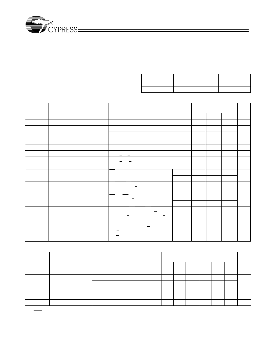
Features
· True dual-ported memory cells which allow
simultaneous reads of the same memory location
· 2K x 16 organization
· 0.65-micron CMOS for optimum speed/power
· High-speed access: 25/35/55 ns
· Low operating power: I
CC
= 150 mA (typ.)
· Fully asynchronous operation
· Master CY7C133 expands data bus width to 32 bits or
more using slave CY7C143
· BUSY output flag on CY7C133; BUSY input flag on
CY7C143
· Available in 68-pin PLCC
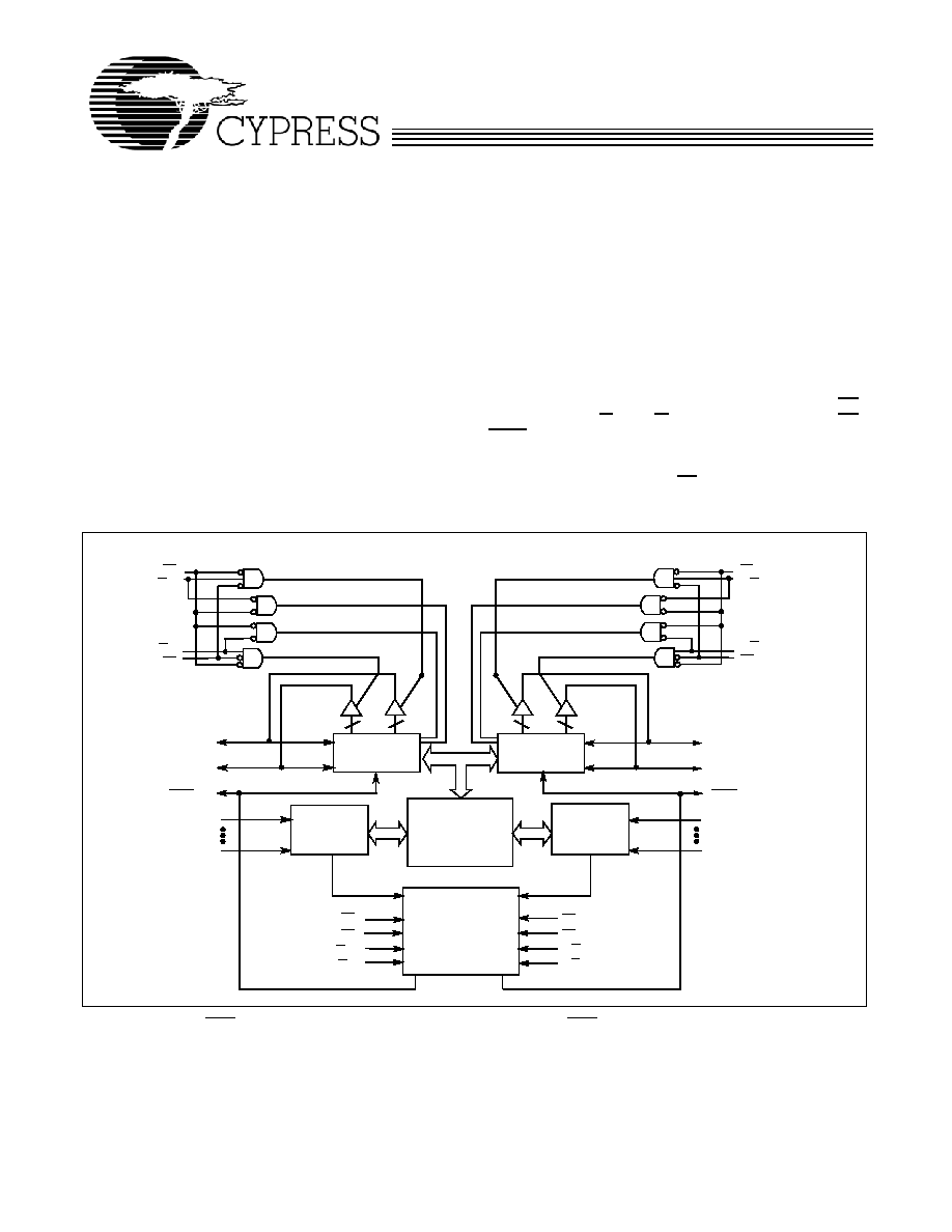
Functional Description
The CY7C133 and CY7C143 are high-speed CMOS 2K by 16
dual-port static RAMs. Two ports are provided permitting
independent access to any location in memory. The CY7C133
can be utilized as either a stand-alone 16-bit dual-port static
RAM or as a master dual-port RAM in conjunction with the
CY7C143 slave dual-port device in systems requiring 32-bit or
greater word widths. It is the solution to applications requiring
shared or buffered data, such as cache memory for DSP,
bit-slice, or multiprocessor designs.
Each port has independent control pins; Chip Enable (CE),
Write Enable (R/W
UB
, R/W
LB
), and Output Enable (OE).
BUSY signals that the port is trying to access the same
location currently being accessed by the other port. An
automatic power-down feature is controlled independently on
each port by the Chip Enable (CE) pin.
The CY7C133 and CY7C143 are available in 68-pin PLCC.
Note:
1.
CY7C133 (Master): BUSY is open drain output and requires pull-up resistor. CY7C143 (Slave): BUSY is input.
R/W
LUB
CE
L
OE
L
A
10L
A
0L
R/W
RUB
CE
R
CE
R
OE
R
CE
L
OE
L
R/W
LUB
R/W
RUB
I/O
8L
I/O
15L
ARBITRATION
LOGIC
(CY7C133 ONLY)
CONTROL
I/O
MEMORY
ARRAY
ADDRESS
DECODER
ADDRESS
DECODER
BUSY
L
[1]
CONTROL
I/O
R/W
LLB
R/W
RLB
I/O
0L
I/O
7L
R/W
RLB
OE
R
A
10R
A
0R
I/O
8R
I/O
15R
BUSY
R
[ ]
I/O
0R
I/O
7R
R/W
LLB
1
Logic Block Diagram
CY7C133
CY7C143
Document #: 38-06036 Rev. *B
Page 2 of 13
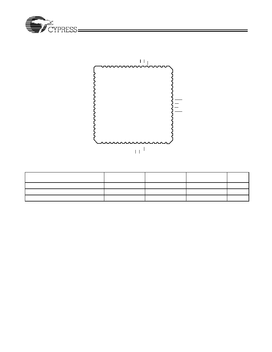
Pin Configuration
I/O
7R
10
11
12
13
14
15
16
17
18
19
20
21
22
23
24
67
Top View
68-Pin LCC/PLCC
60
59
58
57
56
55
54
53
52
51
50
49
48
3132 33 34 35 36 37 38 39 40 41 42 43
5 4 3 2 1 68
66 65 64 63 62 61
A
4L
A
3L
A
2L
A
1L
A
0L
CE
L
BUSY
L
BUSY
R
CE
R
A
0R
I/O
10L
I/O
11L
I/O
12L
I/O
13L
I/O
14L
I/O
15L
V
CC
GND
I/O
0R
I/O
1R
I/O
2R
A
2728 29 30
9 8 7 6
47
46
45
44
A
1R
A
2R
A
3R
A
4R
I/O
3R
I/O
4R
I/O
5R
I/O
6R
25
26
7L
A
8L
A
9L
A
10L
LL
B
V
CC
R/
W
OE
L
I/
O
I/
O
8L
7L
A
A
6R
7R
A
8R
A
9R
A
10
R
R/W
RL
B
OE
R
I/O
8R
GND
A
5L
R/W
RU
B
A
6L
A
5R
I/O
9L
I/
O
I/
O
6L
5L
I/
O
I/
O
4L
3L
I/
O
I/
O
2L
1L
I/
O
0L
LU
B
R/
W
I/O
9R
I/O
10
R
I/O
15
R
I/O
14
R
I/O
13
R
I/O
12
R
I/O
11
R
7C133
7C143
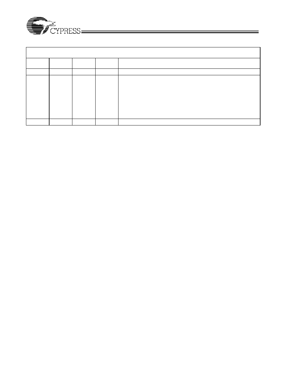
Selection Guide
7C133-25
7C143-25
7C133-35
7C143-35
7C133-55
7C143-55
Unit
Maximum Access Time
25
35
55
ns
Typical Operating Current I
CC
170
160
150
mA
Typical Standby Current for I
SB1
40
30
20
mA
CY7C133
CY7C143
Document #: 38-06036 Rev. *B
Page 3 of 13
Architecture
The CY7C133 (master) and CY7C143 (slave) consist of an
array of 2K words of 16 bits each of dual-port RAM cells, I/O
and address lines, and control signals (CE, OE, R/W). These
control pins permit independent access for reads or writes to any
location in memory. To handle simultaneous writes/reads to the same
location, a BUSY pin is provided on each port. The CY7C133 and
CY7C143 have an automatic power-down feature controlled by CE.
Each port is provided with its own output enable control (OE), which
allows data to be read from the device.
Functional Description
Write Operation
Data must be set up for a duration of t
SD
before the rising edge
of R/W in order to guarantee a valid write. A write operation is
controlled by either the R/W pin (see Write Cycle No. 1 waveform) or
the CE pin (see Write Cycle No. 2 waveform). Two R/W pins (R/W
UB
and R/W
LB
) are used to separate the upper and lower bytes of IO.
Required inputs for non-contention operations are summarized in
Table 1.
If a location is being written to by one port and the opposite
port attempts to read that location, a port-to-port flow-through
delay must occur before the data is read on the output;
otherwise the data read is not deterministic. Data will be valid
on the port t
DDD
after the data is presented on the other port.
Read Operation
When reading the device, the user must assert both the OE
and CE pins. Data will be available t
ACE
after CE or t
DOE
after OE is
asserted.
Busy
The CY7C133 (master) provides on-chip arbitration to resolve
simultaneous memory location access (contention). Table 2
shows a summery of conditions where BUSY is asserted. If both
ports' CEs are asserted and an address match occurs within t
PS
of
each other, the busy logic will determine which port has access. If t
PS
is violated, one port will definitely gain permission to the location, but
which one is not predictable. BUSY will be asserted t
BLA
after an
address match or t
BLC
after CE is taken LOW. The results of all eight
arbitration possibilities are summarized in Table 3. BUSY is an open
drain output and requires a pull-up resistor.
One master and as many slaves as necessary may be
connected in parallel to expand the data bus width in 16 bit
increments. The BUSY output of the master is connected to the
BUSY input of the slave. Writing to slave devices must be delayed
until after the BUSY input has settled (t
BLC
or t
BLA
). Otherwise, the
slave chip may begin a write cycle during a contention
situation.
Flow-Through Operation
The CY7C133/143 has a flow-through architecture that facili-
tates repeating (actually extending) an operation when a
BUSY is received by a losing port. The BUSY signal should be
interpreted as a NOT READY. If a BUSY to a port is active, the
port should wait for BUSY to go inactive, and then extend the
operation it was performing for another cycle. The timing
diagram titled, "Timing waveform with port to port delay" illus-
trates the case where the right port is writing to an address and
the left port reads the same address. The data that the right
port has just written flows through to the left, and is valid either
t
DDD
after the falling edge of the write strobe of the left port, or
t
DDD
after the data being written becomes stable.
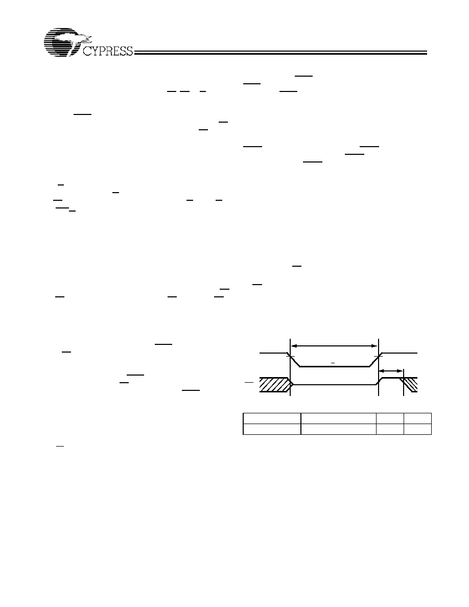
Data Retention Mode
The CY7C133/143 is designed with battery backup in mind.
Data retention voltage and supply current are guaranteed over
temperature. The following rules insure data retention:
1. Chip enable (CE) must be held HIGH during data retention, with-
in V
CC
to V
CC
0.2V.
2. CE must be kept between V
CC
0.2V and 70% of V
CC
during the power-up and power-down transitions.
3. The RAM can begin operation >t
RC
after V
CC
reaches the
minimum operating voltage (4.5V).
Note:
2.
CE = V
CC
, V
in
= GND to V
CC
, T
A
= 25°C. This parameter is guaranteed but not tested.
Timing
Parameter
Test Conditions
[2]
Max.
Unit
ICC
DR1
@ VCC
DR
= 2V
1.5
mA
Data Retention Mode
4.5V
4.5V
V
CC
>
2.0V
V
CC
to V
CC
0.2V
V
CC
CE
t
RC
V
IH
CY7C133
CY7C143
Document #: 38-06036 Rev. *B
Page 4 of 13
Table 1. Non-Contending Read/Write Control
Control
I/O
Operation
R/W
LB
R/W
UB
CE
OE
I/O
0
I/O
8
I/O
9
I/O
17
X
X
H
X
High Z
High Z
Deselected: Power-Down
L
L
L
X
Data In
Data In
Write to Both Bytes
L
H
L
L
Data In
Data Out
Write Lower Byte, Read Upper Byte
H
L
L
L
Data Out
Data In
Read Lower Byte, Write Upper Byte
L
H
L
H
Data In
High Z
Write to Lower Byte
H
L
L
H
High Z
Data In
Write to Upper Byte
H
H
L
L
Data Out
Data Out
Read to Both Bytes
H
H
L
H
High Z
High Z
High Impedance Outputs
Table 2. Address BUSY Arbitration
Inputs
Outputs
Function
CE
L
CE
R
Address
L
Address
R
BUSY
L
BUSY
R
X
X
No Match
H
H
Normal
H
X
Match
H
H
Normal
X
H
Match
H
H
Normal
L
L
Match
Note 3
Note 3
Write Inhibit
[4]
32-Bit Master/Slave Dual-Port Memory Systems
Table 3. Arbitration Results
Case
Port
Winning Port
Result
Left
Right
1
Read
Read
L
Both ports read
2
Read
Read
R
Both ports read
3
Read
Write
L
L port reads OK R port write inhibited
4
Read
Write
R
R port writes OK L port data may be invalid
5
Write
Read
L
L port writes OK R port data may be invalid
6
Write
Read
R
R port reads OK L port write inhibited
7
Write
Write
L
L port writes OK R port write inhibited
8
Write
Write
R
R port writes OK L port write inhibited
Notes:
3.
The loser of the port arbitration will receive BUSY = "L" (BUSY
L
or BUSY
R
= "L"). BUSY
L
and BUSY
R
cannot both be LOW simultaneously.
4.
Writes are inhibited to the left port when BUSY
L
is LOW. Writes are inhibited to the right port when BUSY
R
is LOW.
LEFT
RIGHT
R/W
BUSY
R/W
BUSY
R/W
BUSY
BUSY
R/W
CY7C133
CY7C143
5V
5V
CY7C133
CY7C143
Document #: 38-06036 Rev. *B
Page 5 of 13
Maximum Ratings
(Above which the useful life may be impaired. For user guide-
lines, not tested.)
Storage Temperature
..................................... -
65
°
C to +150
°
C
Ambient Temperature with
Power Applied
.................................................. -
55
°
C to +125
°
C
Supply Voltage to Ground Potential
(Pin 48 to Pin 24)
.................................................-
0.5V to +7.0V
DC Voltage Applied to Outputs
in High-Z State
.....................................................-
0.5V to +7.0V
DC Input Voltage
.................................................-
3.5V to +7.0V
Output Current into Outputs (LOW)............................. 20 mA
Static Discharge Voltage........................................... >2001V
(per MIL-STD-883, Method 3015)
Latch-up Current..................................................... >200 mA
Operating Range
Range
Ambient Temperature
V
CC
Commercial
0
°
C to +70
°
C
5V ± 10%
Industrial
-
40
°
C to +85
°
C
5V ± 10%
Electrical Characteristics
Over the Operating Range
Parameter
Description
Test Conditions
7C133-25
7C143-25
Unit
Min.
Typ.
Max.
V
OH
Output HIGH Voltage
V
CC
= Min., I
OH
= 4.0 mA
2.4
V
V
OL
Output LOW Voltage
I
OL
= 4.0 mA
0.4
V
I
OL
= 16.0 mA
[5]
0.5
V
IH
Input HIGH Voltage
2.2
V
V
IL
Input LOW Voltage
0.8
V
I
IX
Input Leakage Current
GND < V
I
< V
CC
-
5
+5
µ
A
I
OZ
Output Leakage Current
GND < V
O
< V
CC
, Output Disabled
-
5
+5
µ
A
I
OS
Output Short Circuit Current
[6, 7]
V
CC
= Max., V
OUT
= GND
-
200
mA
I
CC
V
CC
Operating Supply Current
CE = V
IL
,
Outputs Open, f = f
MAX
[8]
Com'l
170
250
mA
Ind.
170
290
I
SB1
Standby Current Both Ports, TTL
Inputs
CE
L
and CE
R
> V
IH
, f = f
MAX
[8]
Com'l
40
60
mA
Ind.
40
75
I
SB2
Standby Current One Port, TTL
Inputs
CE
L
or CE
R
> V
IH
, Active Port
Outputs Open, f = f
MAX
[8]
Com'l
100
140
mA
Ind.
100
160
I
SB3
Standby Current Both Ports,
CMOS Inputs
Both Ports CE
L
and CE
R
> V
CC
0.2V, V
IN
> V
CC
0.2V or V
IN
<
0.2V, f = 0
Com'l
3
15
mA
Ind.
3
15
I
SB4
Standby Current One Port,
CMOS Inputs
One Port CE
L
or CE
R
> V
CC
0.2V,
V
IN
> V
CC
0.2V or
V
IN
< 0.2V, Active Port Outputs Open,
f = f
MAX
[8]
Com'l
90
120
mA
Ind.
90
140
Electrical Characteristics
Over the Operating Range (continued)
Parameter
Description
Test Conditions
7C133-35
7C143-35
7C133-55
7C143-55
Unit
Min. Typ. Max. Min.
Typ.
Max.
V
OH
Output HIGH Voltage
V
CC
= Min., I
OH
= 4.0 mA
2.4
2.4
V
V
OL
Output LOW Voltage
I
OL
= 4.0 mA
0.4
0.4
V
I
OL
= 16.0 mA
[5]
0.5
0.5
V
IH
Input HIGH Voltage
2.2
2.2
V
V
IL
Input LOW Voltage
0.8
0.8
V
I
IX
Input Leakage Current GND < V
I
< V
CC
-
5
+5
-
5
+5
µ
A
Notes:
5.
BUSY pin only.
6.
Duration of the short circuit should not exceed 30 seconds.
7.
Tested initially and after any design or process changes that may affect these parameters.
8.
At f=f
MAX
, address and data inputs are cycling at the maximum frequency of read cycle of 1/t
RC
and using AC Test Waveforms input levels of GND to 3V.
CY7C133
CY7C143
Document #: 38-06036 Rev. *B
Page 6 of 13
I
OZ
Output Leakage
Current
GND < V
O
< V
CC
, Output Disabled
-
5
+5
-
5
-
5
µ
A
I
OS
Output Short Circuit
Current
[6, 7]
V
CC
= Max., V
OUT
= GND
-
200
-
200
mA
I
CC
V
CC
Operating Supply
Current
CE = V
IL
,
Outputs Open, f = f
MAX
[8]
Com'l
160
230
150
220
mA
Ind.
160
260
150
250
I
SB1
Standby Current Both
Ports, TTL Inputs
CE
L
and CE
R
> V
IH
, f = f
MAX
[8]
Com'l
30
50
20
40
mA
Ind.
30
65
20
55
I
SB2
Standby Current One
Port, TTL Inputs
CE
L
or CE
R
> V
IH
, Active Port
Outputs Open, f = f
MAX
[8]
Com'l
85
125
75
110
mA
Ind.
85
140
75
125
I
SB3
Standby Current Both
Ports, CMOS Inputs
Both Ports CE
L
and CE
R
>
V
CC
- 0.2V, V
IN
> V
CC
0.2V
or V
IN
< 0.2V, f = 0
Com'l
3
15
3
15
mA
Ind.
3
15
3
15
I
SB4
Standby Current One
Port, CMOS Inputs
One Port CE
L
or CE
R
> V
CC
0.2V, V
IN
> V
CC
0.2V or
V
IN
< 0.2V, Active Port
Outputs Open, f = f
MAX
[8]
Com'l
80
105
70
90
mA
Ind.
80
120
70
105
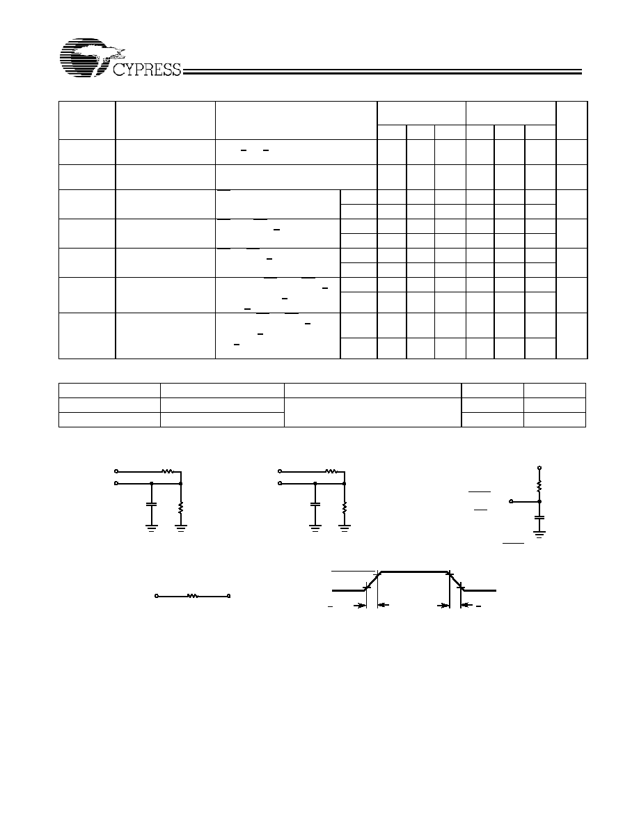
Capacitance
[7]
Parameter
Description
Test Conditions
Max.
Unit
C
IN
Input Capacitance
T
A
= 25
°
C, f = 1 MHz, V
CC
= 5.0V
10
pF
C
OUT
Output Capacitance
10
pF
AC Test Loads and Waveforms
Electrical Characteristics
Over the Operating Range (continued)
Parameter
Description
Test Conditions
7C133-35
7C143-35
7C133-55
7C143-55
Unit
Min. Typ. Max. Min.
Typ.
Max.
3.0V
5V
OUTPUT
R1893
R2
347
30 pF
INCLUDING
JIG AND
SCOPE
GND
90%
90%
10%
5V
OUTPUT
R1893
R2
347
5 pF
INCLUDING
JIG AND
SCOPE
(a)
(b)
OUTPUT
1.40V
Equivalent to:
TH ÉVENIN EQUIVALENT
5V
281
30 pF
BUSY
OR
INT
BUSY Output Load
(CY7C133 ONLY)
10%
ALL INPUT PULSES
250
< 3 ns
< 3 ns
CY7C133
CY7C143
Document #: 38-06036 Rev. *B
Page 7 of 13
Switching Characteristics
Over the Operating Range
[9]
Parameter
Description
7C133-25
7C143-25
7C133-35
7C143-35
7C133-55
7C143-55
Unit
Min.
Max.
Min.
Max.
Min.
Max.
Read Cycle
t
RC
Read Cycle Time
25
35
55
ns
t
AA
Address to Data Valid
[10]
25
35
55
ns
t
OHA
Data Hold from Address Change
0
0
0
ns
t
ACE
CE LOW to Data Valid
[10]
25
35
55
ns
t
DOE
OE LOW to Data Valid
[10]
20
25
30
ns
t
LZOE
OE LOW to Low Z
[11, 12,13]
3
3
3
ns
t
HZOE
OE HIGH to High Z
[11, 12,13]
15
20
25
ns
t
LZCE
CE LOW to Low Z
[11, 12,13]
3
5
5
ns
t
HZCE
CE HIGH to High Z
[11, 12,13]
15
20
20
ns
t
PU
CE LOW to Power-Up
[13]
0
0
0
ns
t
PD
CE HIGH to Power-Down
[13]
25
25
25
ns
Write Cycle
[14]
t
WC
Write Cycle Time
25
35
55
ns
t
SCE
CE LOW to Write End
20
25
40
ns
t
AW
Address Set-up to Write End
20
25
40
ns
t
HA
Address Hold from Write End
2
2
2
ns
t
SA
Address Set-up to Write Start
0
0
0
ns
t
PWE
R/W Pulse Width
20
25
35
ns
t
SD
Data Set-up to Write End
15
20
20
ns
t
HD
Data Hold from Write End
0
0
0
ns
t
HZWE
R/W LOW to High Z
[12,13]
15
20
20
ns
t
LZWE
R/W HIGH to Low Z
[12,13]
0
0
0
ns
Busy/Interrupt Timing (for master CY7C133)
t
BLA
BUSY Low from Address Match
25
35
50
ns
t
BHA
BUSY High from Address Mismatch
20
30
40
ns
t
BLC
BUSY Low from CE LOW
20
25
35
ns
t
BHC
BUSY High from CE HIGH
20
20
30
ns
t
WDD
Write Pulse to Data Delay
[15]
50
60
80
ns
t
DDD
Write Data Valid to Read Data Valid
[15]
35
45
55
ns
t
BDD
BUSY High to Valid Data
[16]
Note 16
Note 16
Note 16
ns
t
PS
Arbitration Priority Set Up Time
[17]
5
5
5
ns
Busy Timing (for slave CY7C143)
t
WB
Write to BUSY
[18]
0
0
0
ns
t
WH
Write Hold After BUSY
[19]
20
25
30
ns
t
WDD
Write Pulse to Data Delay
[20]
50
60
80
ns
t
DDD
Write Data Valid to Read Data Valid
[20]
35
45
55
ns
Notes:
9.
Test conditions assume signal transition times of 5 ns or less, timing reference levels of 1.5V, input pulse levels of 0 to 3.0V and output loading of the specified
I
OL
/I
OH,
and 30-pF load capacitance.
10. AC Test Conditions use V
OH
= 1.6V and V
OL
= 1.4V.
11. At any given temperature and voltage condition for any given device, t
LZCE
is less than t
HZCE
and t
LZOE
is less than t
HZOE
.
12. t
LZCE
, t
LZWE
, t
HZOE
, t
LZOE
, t
HZCE
and t
HZWE
are tested with C
L
= 5 pF as in part (b) of AC Test Loads. Transition is measured ±500 mV from steady state voltage.
13. This parameter is guaranteed but not tested.
14. The internal write time of the memory is defined by the overlap of CS LOW and R/W LOW. Both signals must be LOW to initiate a write and either signal
can terminate a write by going HIGH. The data input set-up and hold timing should be referenced to the rising edge of the signal that terminates the write.
15. Port-to-port delay through RAM cells from writing port to reading port. Refer to timing waveform of "Read with BUSY, Master: CY7C133."
16. t
BDD
is a calculated parameter and is greater of 0,t
WDD
t
WP
(actual) or t
DDD
t
DW
(actual).
17. To ensure that the earlier of the two ports wins.
18. To ensure that write cycle is inhibited during contention.
19. To ensure that a write cycle is completed after contention.
20. Port-to-port delay through RAM cells from writing port to reading port. Refer to timing waveform of "Read with Port-to-port Delay."
CY7C133
CY7C143
Document #: 38-06036 Rev. *B
Page 8 of 13
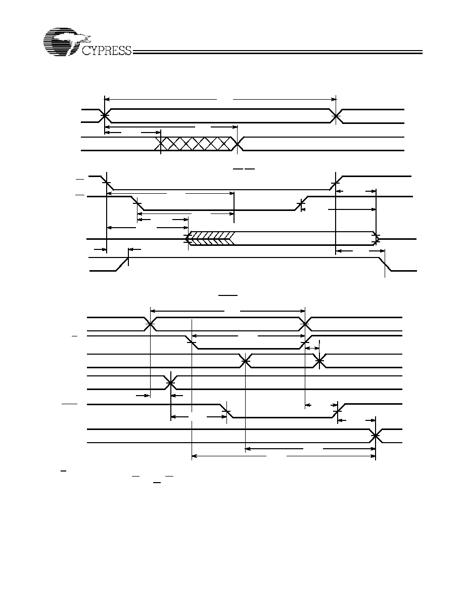
Switching Waveforms
Read Cycle No.1
[21, 22]
Read Cycle No. 2
[21, 23]
Read Cycle No. 3
[22]
Note:
21. R/W is HIGH for read cycle.
22. Device is continuously selected, CE = V
IL
and OE = V
IL
.
23. Address valid prior to or coincidence with CE transition LOW.
t
RC
t
AA
t
OHA
DATA VALID
PREVIOUS DATA VALID
DATA OUT
ADDRESS
Either Port Address Access
t
ACE
t
LZOE
t
DOE
t
HZOE
t
HZCE
DATA VALID
DATA OUT
CE
OE
t
LZCE
t
PU
I
CC
I
SB
t
PD
Either Port CE/OE Access
t
BHA
t
BDD
VALID
t
DDD
t
WDD
ADDRESS MATCH
ADDRESS MATCH
R/W
R
ADDRESS
R
D
INR
ADDRESS
L
BUSY
L
DOUT
L
t
PS
t
BLA
Read with BUSY (for master CY7C133)
t
RC
t
PWE
VALID
t
HD
CY7C133
CY7C143
Document #: 38-06036 Rev. *B
Page 9 of 13
Timing Waveform of Read with Port-to-port Delay No. 4 (for slave CY7C143)
[24, 25, 26]
Write Cycle No. 1 (OE Three-States Data I/Os - Either Port)
[17, 27]
Notes:
24. Assume BUSY input at V
IH
for the writing port and at V
IL
for the reading port.l
25. Write cycle parameters should be adhered to in order to ensure proper writing.
26. Device is continuously enabled for both ports.
27. If OE is LOW during a R/W controlled write cycle, the write pulse width must be the larger of t
PWE
or t
HZWE
+ t
SD
to allow the data I/O pins to enter high
impedance and for data to be placed on the bus for the required t
SD
.
Switching Waveforms
(continued)
VALID
t
DDD
MATCH
MATCH
R/W
R
D
INR
DOUT
L
t
WC
t
WP
VALID
t
WDD
t
DH
t
DW
ADDRESS
L
ADDRESS
R
t
AW
t
WC
DATA VALID
HIGH IMPEDANCE
t
SCE
t
SA
t
PWE
t
HD
t
SD
t
HA
t
HZOE
Either Port
R/W
CE
ADDRESS
DATA
IN
OE
D
OUT
CY7C133
CY7C143
Document #: 38-06036 Rev. *B
Page 10 of 13
Write Cycle No. 2 (R/W Three-States Data I/Os--Either Port)
[23, 28]
Busy Timing Diagram No. 1 (CE Arbitration)
Note:
28. If the CE LOW transition occurs simultaneously with or after the R/W LOW transition, the outputs remain in the high-impedance state.
Switching Waveforms
(continued)
t
AW
t
WC
t
SCE
t
SA
t
PWE
t
HD
t
SD
t
HZWE
Either Port
t
HA
HIGH IMPEDANCE
DATA VALID
t
LZWE
ADDRESS
CE
R/W
DATA
IN
DATA
OUT
ADDRESS
ADDRESS MATCH
t
PS
CE
L
Valid First:
t
BLC
t
BHC
ADDRESS MATCH
t
PS
t
BLC
t
BHC
CE
R
Valid First:
L,R
BUSY
R
CE
L
CE
R
BUSY
L
CE
R
CE
L
ADDRESS
L,R
CY7C133
CY7C143
Document #: 38-06036 Rev. *B
Page 11 of 13
Busy Timing Diagram No. 2 (Address Arbitration)
Busy Timing Diagram No. 3
Switching Waveforms
(continued)
Left Address Valid First:
ADDRESS MATCH
t
PS
ADDRESS
L
BUSY
R
ADDRESS MISMATCH
t
RC
or t
WC
t
BLA
t
BHA
ADDRESS
R
ADDRESS MATCH
ADDRESS MISMATCH
t
PS
ADDRESS
L
BUSY
L
t
RC
or t
WC
t
BLA
t
BHA
ADDRESS
R
Right Address Valid First:
t
PWE
t
WB
t
WH
Write with BUSY (For Slave CY7C143)
BUSY
R/W
CE
CY7C133
CY7C143
Document #: 38-06036 Rev. *B
Page 12 of 13
© Cypress Semiconductor Corporation, 2004. The information contained herein is subject to change without notice. Cypress Semiconductor Corporation assumes no responsibility for the use
of any circuitry other than circuitry embodied in a Cypress product. Nor does it convey or imply any license under patent or other rights. Cypress products are not warranted nor intended to be
used for medical, life support, life saving, critical control or safety applications, unless pursuant to an express written agreement with Cypress. Furthermore, Cypress does not authorize its
products for use as critical components in life-support systems where a malfunction or failure may reasonably be expected to result in significant injury to the user. The inclusion of Cypress
products in life-support systems application implies that the manufacturer assumes all risk of such use and in doing so indemnifies Cypress against all charges.
All product and company names mentioned in this document are the trademarks of their respective holders.
Ordering Information
2K x 16 Master Dual-Port SRAM
Speed
(ns)
Ordering Code
Package
Name
Package Type
Operating
Range
25
CY7C133-25JC
J81
68-Lead Plastic Leaded Chip Carrier
Commercial
CY7C133-25JI
J81
68-Lead Plastic Leaded Chip Carrier
Industrial
35
CY7C133-35JC
J81
68-Lead Plastic Leaded Chip Carrier
Commercial
CY7C133-35JI
J81
68-Lead Plastic Leaded Chip Carrier
Industrial
55
CY7C133-55JC
J81
68-Lead Plastic Leaded Chip Carrier
Commercial
Package Diagram
68-Lead Plastic Leaded Chip Carrier J81
51-85005-*A
CY7C133
CY7C143
Document #: 38-06036 Rev. *B
Page 13 of 13
Document History Page
Document Title: CY7C133/CY7C143 2K x 16 Dual-Port Static RAM
Document Number: 38-06036
REV.
ECN NO.
Issue
Date
Orig. of
Change
Description of Change
**
110178
09/22/01
SZV
Change from Spec number: 38-00414 to 38-06036
*A
127954
08/27/03
FSG
Logic Block Diagram: fixed busy I/O flag on devices (typo)
Removed obsolete parts from ordering information table:
CY7C133-55JI
CY7C143-25JC
CY7C143-25JI
CY7C143-35JC
CY7C143-35JI
CY7C143-55JC
CY7C143-55JI
*B
236761
See ECN
YDT
Removed cross information from features section