512K x 36/1M x 18 Pipelined SRAM
with NoBLTM Architecture
CY7C1372BV25
CY7C1370BV25
Cypress Semiconductor Corporation
∑
3901 North First Street
∑
San Jose
∑
CA 95134
∑
408-943-2600
Document #: 38-05252 Rev. *A
Revised January 18, 2003
Features
∑ Zero Bus Latency, no dead cycles between Write and
Read cycles
∑ Fast clock speed: 200,167, 150, and 133 MHz
∑ Fast access time: 3.0, 3.4, 3.8, 4.2 ns
∑ Internally synchronized registered outputs eliminate
the need to control OE
∑ Single 2.5V +5%
∑ Single WE (Read/Write) control pin
∑ Positive clock-edge triggered, address, data, and
control signal registers for fully pipelined applications
∑ Interleaved or linear 4-word burst capability
∑ Individual byte Write (BWS
a
≠BWS
d
) control (may be
tied LOW)
∑ CEN pin to enable clock and suspend operations
∑ Three chip enables for simple depth expansion
∑ JTAG boundary scan for BGA packaging version
∑ Available in 119-ball bump BGA and 100-pin TQFP
packages
∑ Automatic power-down available using zz mode or CE
deselect
Functional Description
The CY7C1370BV25 and CY7C1372BV25 SRAMs are
designed to eliminate dead cycles when transitions from
READ to WRITE or vice versa. These SRAMs are optimized
for 100 percent bus utilization and achieves Zero Bus Latency.
They integrate 524,288 ◊ 36 and 1,048,576 ◊ 18 SRAM cells,
respectively, with advanced synchronous peripheral circuitry
and a 2-bit counter for internal burst operation. The Cypress
Synchronous Burst SRAM family employs high-speed,
low-power CMOS designs using advanced single layer
polysilicon, threelayer metal technology. Each memory cell
consists of six transistors.
All synchronous inputs are gated by registers controlled by a
positive-edge-triggered Clock Input (CLK). The synchronous
inputs include all addresses, all data inputs, depth-expansion
Chip Enables (CE
1
, CE
2
and CE
3
), cycle start input (ADV/LD),
Clock Enable (CEN), Byte Write Selects (BWS
a
, BWS
b
, BWS
c
and BWS
d
), and Read-Write control (WE). BWS
c
and BWS
d
apply to CY7C1370BV25 only.
Address and control signals are applied to the SRAM during
one clock cycle, and two cycles later, its associated data
occurs, either Read or Write.
A Clock Enable (CEN) pin allows operation of the
CY7C1370BV25/CY7C1372BV25 to be suspended as long as
necessary. All synchronous inputs are ignored when (CEN) is
HIGH and the internal device registers will hold their previous
values.
There are three Chip Enable (CE
1
, CE
2
, CE
3
) pins that allow
the user to deselect the device when desired. If any one of
these three are not active when ADV/LD is LOW, no new
memory operation can be initiated and any burst cycle in
progress is stopped. However, any pending data transfers
(Read or Write) will be completed. The data bus will be in
high-impedance state two cycles after chip is deselected or a
Write cycle is initiated.
The CY7C1370BV25 and CY7C1372BV25 have an on-chip
two-bit burst counter. In the burst mode, the CY7C1370BV25
and CY7C1372BV25 provide four cycles of data for a single
address presented to the SRAM. The order of the burst
sequence is defined by the MODE input pin. The MODE pin
selects between linear and interleaved burst sequence. The
ADV/LD signal is used to load a new external address
(ADV/LD = LOW) or increment the internal burst counter
(ADV/LD = HIGH)
Output Enable (OE) and burst sequence select (MODE) are
the asynchronous signals. OE can be used to disable the
outputs at any given time. ZZ may be tied to LOW if it is not
used.
Four pins are used to implement JTAG test capabilities. The
JTAG circuitry is used to serially shift data to and from the
device. JTAG inputs use LVTTL/LVCMOS levels to shift data
during this testing mode of operation.
CLK
A
x
CEN
WE
BWS
x
CE
1
CE
CE
2
OE
256K ◊ 36/
MEMORY
ARRAY
Logic Block Diagram
DQ
x
Data-In REG.
Q
D
CE
CONTROL
and WRITE
LOGIC
3
ADV/LD
Mode
DP
x
CY7C1370
CY7C1372
A
X
DQ
X
DP
X
BWS
X
512K ◊ 18
X = 18:0
X = 19:0
X = a, b, c, d
X = a, b
X = a, b
X = a, b
X = a, b, c, d
X = a, b, c, d
OUT
O
UT
R
E
GI
ST
ER
S
and LO
G
I
C
CY7C1372BV25
CY7C1370BV25
Document #: 38-05252 Rev. *A
Page 5 of 26
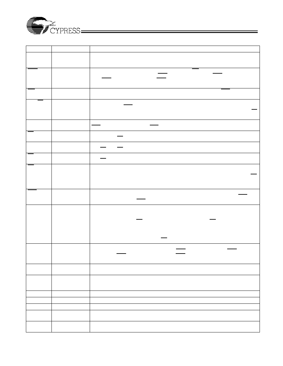
Pin Definitions
Pin Name
I/O Type
Pin Description
A0
A1
A
Input-
Synchronous
Address Inputs used to select one of the 524,288/1048576 address locations. Sampled at
the rising edge of CLK.
BWS
a
BWS
b
BWS
c
BWS
d
Input-
Synchronous
Byte Write Select Inputs, active LOW. Qualified with WE to conduct writes to the SRAM.
Sampled on the rising edge of CLK. BWS
a
controls DQ
a
and DP
a
, BWS
b
controls DQ
b
and
DP
b
, BWS
c
controls DQ
c
and DP
c
, BWS
d
controls DQ
d
and DP
d
.
WE
Input-
Synchronous
Write Enable Input, active LOW. Sampled on the rising edge of CLK if CEN is active LOW.
This signal must be asserted LOW to initiate a Write sequence.
ADV/LD
Input-
Synchronous
Advance/Load Input used to advance the on-chip address counter or load a new address.
When HIGH (and CEN is asserted LOW) the internal burst counter is advanced. When LOW,
a new address can be loaded into the device for an access. After being deselected, ADV/LD
should be driven LOW in order to load a new address.
CLK
Input-Clock
Clock Input. Used to capture all synchronous inputs to the device. CLK is qualified with
CEN. CLK is only recognized if CEN is active LOW.
CE
1
Input-
Synchronous
Chip Enable 1 Input, active LOW. Sampled on the rising edge of CLK. Used in conjunction
with CE
2
and CE
3
to select/deselect the device.
CE
2
Input-
Synchronous
Chip Enable 2 Input, active HIGH. Sampled on the rising edge of CLK. Used in conjunction
with CE
1
and CE
3
to select/deselect the device.
CE
3
Input-
Synchronous
Chip Enable 3 Input, active LOW. Sampled on the rising edge of CLK. Used in conjunction
with CE
1
and
CE
2
to select/deselect the device.
OE
Input-
Asynchronous
Output Enable, active LOW. Combined with the synchronous logic block inside the device
to control the direction of the I/O pins. When LOW, the I/O pins are allowed to behave as
outputs. When deasserted HIGH, I/O pins are three-stated, and act as input data pins. OE
is masked during the data portion of a Write sequence, during the first clock when emerging
from a deselected state and when the device has been deselected.
CEN
Input-
Synchronous
Clock Enable Input, active LOW. When asserted LOW the clock signal is recognized by
the SRAM. When deasserted HIGH the clock signal is masked. Since deasserting CEN does
not deselect the device, CEN can be used to extend the previous cycle when required.
DQ
a
DQ
b
DQ
c
DQ
d
I/O-
Synchronous
Bidirectional Data I/O Lines. As inputs, they feed into an on-chip data register that is
triggered by the rising edge of CLK. As outputs, they deliver the data contained in the memory
location specified by A
X
during the previous clock rise of the Read cycle. The direction of
the pins is controlled by OE and the internal control logic. When OE is asserted LOW, the
pins can behave as outputs. When HIGH, DQ
a
≠DQ
d
are placed in a three-state condition.
The outputs are automatically three-stated during the data portion of a Write sequence,
during the first clock when emerging from a deselected state, and when the device is
deselected, regardless of the state of OE. DQ a,b,c and d are eight bits wide
DP
a
DP
b
DP
c
DP
d
I/O-
Synchronous
Bidirectional Data Parity I/O Lines. Functionally, these signals are identical to DQ
[31:0]
.
During Write sequences, DP
a
is controlled by BWS
a
, DP
b
is controlled by BWS
b
, DP
c
is
controlled by BWS
c
, and DP
d
is controlled by BWS
d
.DP a,b,c and d are 1 bit wide
ZZ
Input-
Asynchronous
ZZ "sleep" Input. This active HIGH input places the device in a non-time critical "sleep"
condition with data integrity preserved.
MODE
Input Pin
Mode Input. Selects the burst order of the device. Tied HIGH selects the interleaved burst
order. Pulled LOW selects the linear burst order. MODE should not change states during
operation. When left floating MODE will default HIGH, to an interleaved burst order.
V
DD
Power Supply
Power supply inputs to the core of the device.
V
DDQ
I/O Power Supply
Power supply for the I/O circuitry.
V
SS
Ground
Ground for the device. Should be connected to ground of the system.
TDO
JTAG serial output
Synchronous
Serial data-out to the JTAG circuit. Delivers data on the negative edge of TCK (BGA only).
TDI
JTAG serial input
Synchronous
Serial data-In to the JTAG circuit. Sampled on the rising edge of TCK (BGA Only).