512K x 36 / 1 Mb x 18 Flow-Thru SRAM
CY7C1381BV25
CY7C1383BV25
PRELIMINARY
Cypress Semiconductor Corporation
∑
3901 North First Street
∑
San Jose
∑
CA 95134
∑
408-943-2600
July 2, 2001
1
Features
∑ Fast access times: 6.5, 7.5, 8.5 ns
∑ Fast clock speed: 133, 117, 100 MHz
∑ Provide high-performance 3-1-1-1 access rate
∑ Optimal for depth expansion
∑ 2.5V (+5%) power supply
∑ Common data inputs and data outputs
∑ Byte Write Enable and Global Write control
∑ Chip enable for address pipeline
∑ Address, data, and control registers
∑ Internally self-timed Write Cycle
∑ Burst control pins (interleaved or linear burst
sequence)
∑ Automatic power-down for portable applications
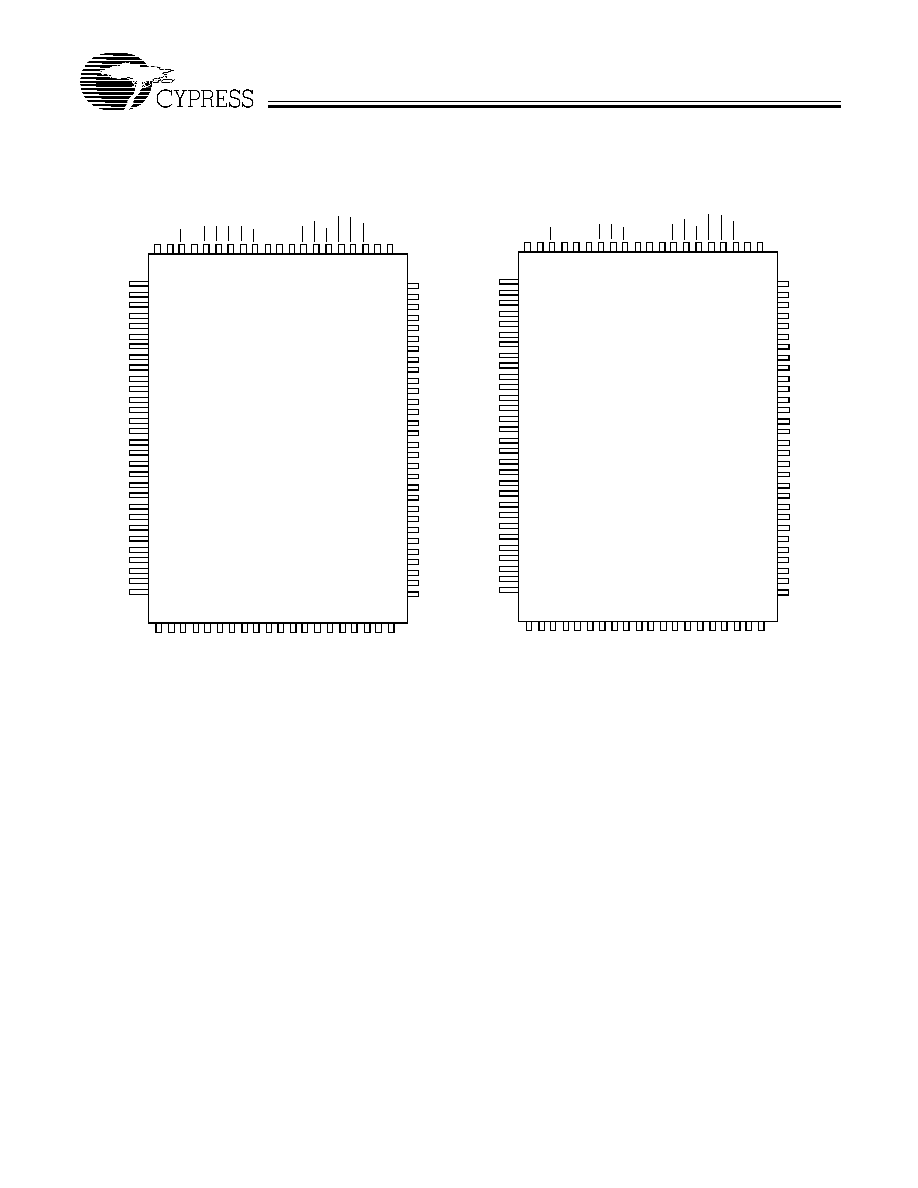
∑ High-density, high-speed packages
∑ JTAG boundary scan for BGA packaging version
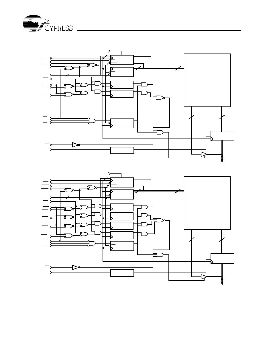
Functional Description
The Cypress Synchronous Burst SRAM family employs
high-speed, low power CMOS designs using advanced single
layer polysilicon, three-layer metal technology. Each memory
cell consists of six transistors.
The CY7C1381BV25 and CY7C1383BV25 SRAMs integrate
524,288x36 and 1,048,576x18SRAM cells with advanced syn-
chronous peripheral circuitry and a 2-bit counter for internal
burst operation. All synchronous inputs are gated by registers
controlled by a positive-edge-triggered Clock Input (CLK). The
synchronous inputs include all addresses, all data inputs, ad-
dress-pipelining Chip Enable (CE), Burst Control Inputs (AD-
SC, ADSP, and ADV), Write Enables (BWa, BWb, BWc,
BWd,and BWe), and Global Write (GW).
... Asynchronous inputs include the Output Enable (OE) and
burst Mode Control (MODE). The Data Outputs (Q), enabled
by OE, are also asynchronous.
Addresses and chip enables are registered with either Ad-
dress Status Processor (ADSP) or Address Status Controller
(ADSC) input pins. Subsequent burst addresses can be inter-
nally generated as controlled by the Burst Advance Pin (ADV).
Address, data inputs, and write controls are registered on-chip
to initiate self-timed WRITE cycle. WRITE cycles can be one
to four bytes wide as controlled by the write control inputs.
Individual byte write allows individual byte to be written. BWa
controls DQ1≠DQ8 and DQP1. BWb controls DQ9≠DQ16 and
DQP2. BWc controls DQ17≠DQ24and DQP3. BWd controls
DQ25≠DQ32 and DQP4. BWa, BWb BWc, and BWd can be
active only with BWe being LOW. GW being LOW causes all
bytes to be written. WRITE pass-through capability allows writ-
ten data available at the output for the immediately next READ
cycle. This device also incorporates pipelined enable circuit for
easy depth expansion without penalizing system performance.
All inputs and outputs of the CY7C1381BV25 and the
CY7C1383BV25 are JEDEC standard JESD8-5 compatible.
Shaded areas contain advance information.
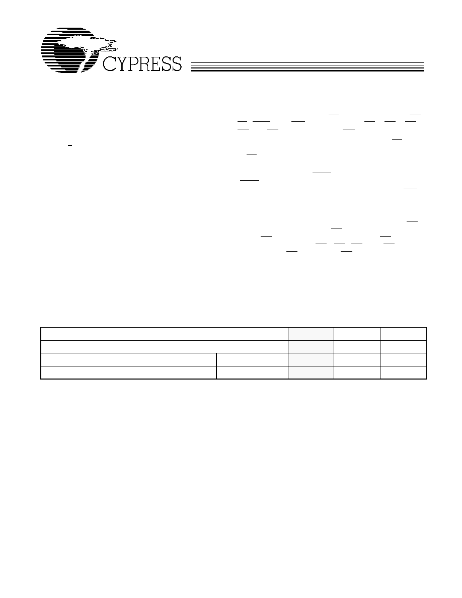
Selection Guide
133 MHz
117 MHz
100 MHz
Maximum Access Time (ns)
6.5
7.5
8.5
Maximum Operating Current (mA)
Commercial
200
175
150
Maximum CMOS Standby Current (mA)
30
30
30
CY7C1381BV25
CY7C1383BV25
PRELIMINARY
5
Pin Definitions
Name
I/O
Description
A0
A1
A
Input-
Synchronous
Address Inputs used to select one of the address locations. Sampled at the
rising edge of the CLK if ADSP or ADSC is active LOW, and CE
1
, CE
2
, and
CE
3
are sampled active. A
[1:0]
feed the 2-bit counter.
BWa
BWb
BWc
BWd
Input-
Synchronous
Byte Write Select Inputs, active LOW. Qualified with BWE to conduct byte
writes to the SRAM. Sampled on the rising edge of CLK.
GW
Input-
Synchronous
Global Write Enable Input, active LOW. When asserted LOW on the rising
edge of CLK, a global write is conducted (ALL bytes are written, regardless of
the values on BW
a,b,c,d
and BWE).
BWE
Input-
Synchronous
Byte Write Enable Input, active LOW. Sampled on the rising edge of CLK. This
signal must be asserted LOW to conduct a byte write.
CLK
Input-Clock
Clock Input. Used to capture all synchronous inputs to the device. Also used
to increment the burst counter when ADV is asserted LOW, during a burst
operation.
CE
1
Input-
Synchronous
Chip Enable 1 Input, active LOW. Sampled on the rising edge of CLK. Used
in conjunction with CE
2
and CE
3
to select/deselect the device. ADSP is ig-
nored if CE
1
is HIGH. (TQFP Only)
CE
2
Input-
Synchronous
Chip Enable 2 Input, active HIGH. Sampled on the rising edge of CLK. Used
in conjunction with CE
1
and CE
3
to select/deselect the device. (TQFP Only)
CE
3
Input-
Synchronous
Chip Enable 3 Input, active LOW. Sampled on the rising edge of CLK. Used
in conjunction with CE
1
and
CE
2
to select/deselect the device.
OE
Input-
Asynchronous
Output Enable, asynchronous input, active LOW. Controls the direction of the
I/O pins. When LOW, the I/O pins behave as outputs. When deasserted HIGH,
I/O pins are three-stated, and act as input data pins. OE is masked during the
first clock of a read cycle when emerging from a deselected state.
ADV
Input-
Synchronous
Advance Input signal, sampled on the rising edge of CLK. When asserted, it
automatically increments the address in a burst cycle.
ADSP
Input-
Synchronous
Address Strobe from Processor, sampled on the rising edge of CLK. When
asserted LOW, A is captured in the address registers. A
[1:0]
are also loaded
into the burst counter. When ADSP and ADSC are both asserted, only ADSP
is recognized. ASDP is ignored when CE
1
is deasserted HIGH.
ADSC
Input-
Synchronous
Address Strobe from Controller, sampled on the rising edge of CLK. When
asserted LOW, A
[x:0]
is captured in the address registers. A
[1:0]
are also loaded
into the burst counter. When ADSP and ADSC are both asserted, only ADSP
is recognized.
MODE
Input-
Static
Selects burst order. When tied to GND selects linear burst sequence. When
tied to V
DDQ
or left floating selects interleaved burst sequence. This is a strap
pin and should remain static during device operation.
ZZ
Input-
Asynchronous
ZZ "sleep" Input. This active HIGH input places the device in a non-time critical
"sleep" condition with data integrity preserved.
DQa, DQPa
DQb, DQPb
DQc, DQPc
DQd, DQPd
I/O-
Synchronous
Bidirectional Data I/O lines. As inputs, they feed into an on-chip data register
that is triggered by the rising edge of CLK. As outputs, they deliver the data
contained in the memory location specified by A during the previous clock rise
of the read cycle. The direction of the pins is controlled by OE. When OE is
asserted LOW, the pins behave as outputs. When HIGH, DQa≠DQd and DQ-
Pa≠DQPd are placed in a three-state condition.
TDO
JTAG serial
output
Synchronous
Serial data-out to the JTAG circuit. Delivers data on the negative edge of TCK
(BGA Only).
TDI
JTAG serial
input
Synchronous
Serial data-In to the JTAG circuit. Sampled on the rising edge of TCK (BGA
Only).