Äîêóìåíòàöèÿ è îïèñàíèÿ www.docs.chipfind.ru
32K x 8 3.3V Static RAM
CY7C1399B
Cypress Semiconductor Corporation
·
3901 North First Street
·
San Jose
·
CA 95134
·
408-943-2600
Document #: 38-05071 Rev. *C
Revised June 19, 2001
C1399B
Features
· Single 3.3V power supply
· Ideal for low-voltage cache memory applications
· High speed
-- 10/12/15 ns
· Low active power
-- 216 mW (max.)
· Low-power alpha immune 6T cell
· Plastic SOJ and TSOP packaging
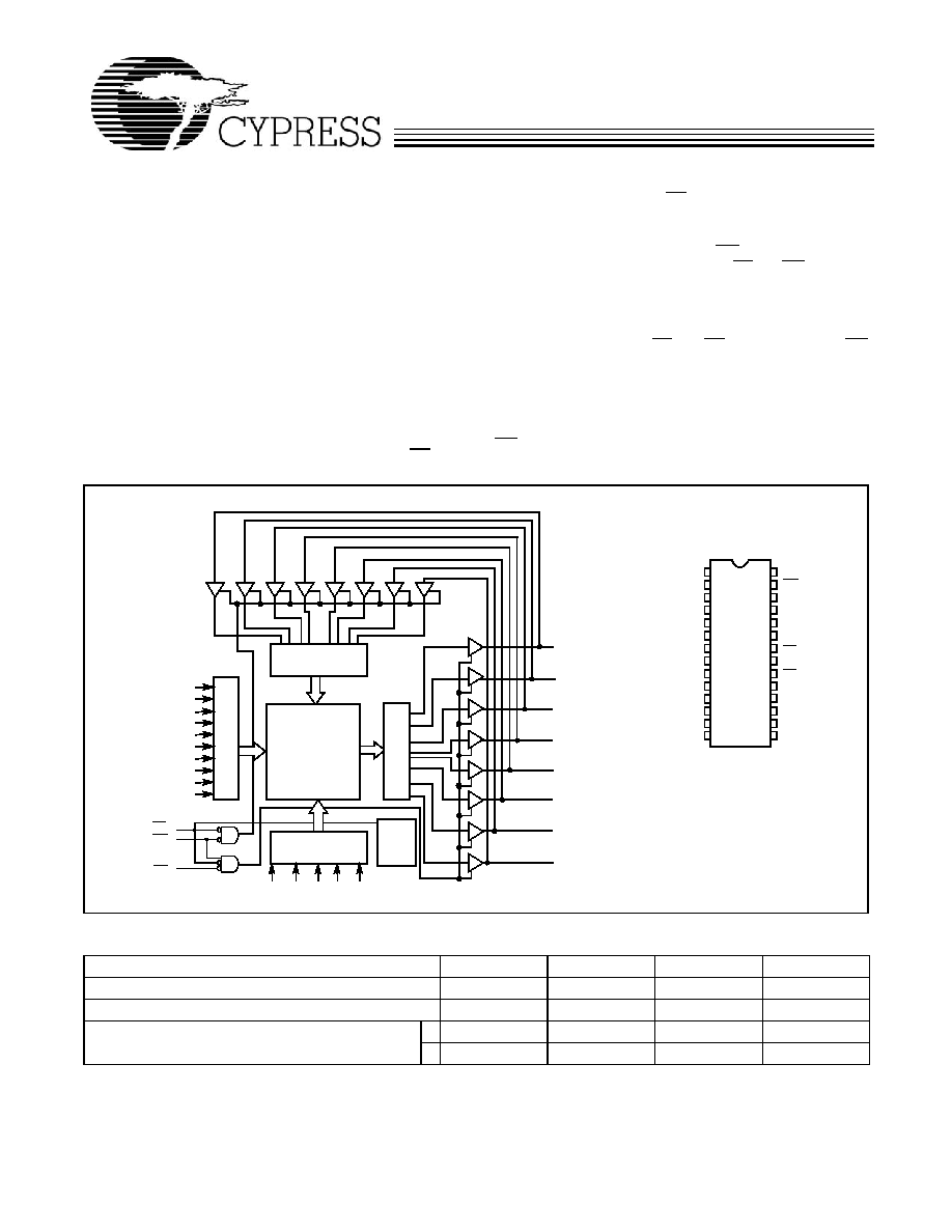
Functional Description
[1]
The CY7C1399B is a high-performance 3.3V CMOS Static
RAM organized as 32,768 words by 8 bits. Easy memory ex-
pansion is provided by an active LOW Chip Enable (CE) and
active LOW Output Enable (OE) and three-state drivers. The
device has an automatic power-down feature, reducing the
power consumption by more than 95% when deselected.
An active LOW Write Enable signal (WE) controls the writing/
reading operation of the memory. When CE and WE inputs are
both LOW, data on the eight data input/output pins (I/O
0
through I/O
7
) is written into the memory location addressed by
the address present on the address pins (A
0
through A
14
).
Reading the device is accomplished by selecting the device
and enabling the outputs, CE and OE active LOW, while WE
remains inactive or HIGH. Under these conditions, the con-
tents of the location addressed by the information on address
pins is present on the eight data input/output pins.
The input/output pins remain in a high-impedance state unless
the chip is selected, outputs are enabled, and Write Enable
(WE) is HIGH. The CY7C1399B is available in 28-pin standard
300-mil-wide SOJ and TSOP Type I packages.
Note:
1.
For guidelines on SRAM system design, please refer to the `System Design Guidelines' Cypress application note, available on the internet at www.cypress.com.
Logic Block Diagram
Pin Configurations
1
2
3
4
5
6
7
8
9
10
11
14
15
16
20
19
18
17
21
24
23
22
Top View
SOJ
12
13
25
28
27
26
GND
A
6
A
7
A
8
A
9
A
10
A
11
A
12
A
13
WE
V
CC
A
4
A
3
A
2
A
1
I/O
7
I/O
6
I/O
5
I/O
4
A
14
A
5
I/O
0
I/O
1
I/O
2
CE
OE
A
0
I/O
3
A
1
A
2
A
3
A
4
A
5
A
6
A
7
A
8
COLUMN
DECODER
ROW DECODE
R
SEN
SE AM
PS
INPUT BUFFER
POWER
DOWN
WE
OE
I/O
0
CE
I/O
1
I/O
2
I/O
3
32K x 8
ARRAY
I/O
7
I/O
6
I/O
5
I/O
4
A
9
A
0
A
11
A
13
A
12
A
14
A
10
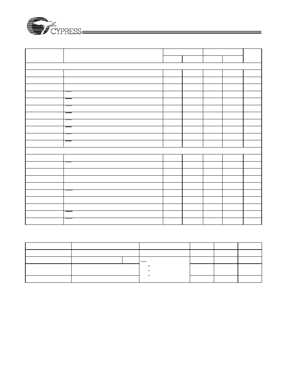
Selection Guide
1399B-10
1399B-12
1399B-15
1399B-20
Maximum Access Time (ns)
10
12
15
20
Maximum Operating Current (mA)
60
55
50
45
Maximum CMOS Standby Current (
µ
A)
500
500
500
500
L
50
50
50
50
CY7C1399B
Document #: 38-05071 Rev. *C
Page 2 of 10
Maximum Ratings
(Above which the useful life may be impaired. For user guide-
lines, not tested.)
Storage Temperature ................................. 65
°
C to +150
°
C
Ambient Temperature with
Power Applied............................................. 55
°
C to +125
°
C
Supply Voltage on V
CC
to Relative GND
[2]
.... 0.5V to +4.6V
DC Voltage Applied to Outputs
in High Z State
[2]
....................................0.5V to V
CC
+ 0.5V
DC Input Voltage
[2]
.................................0.5V to V
CC
+ 0.5V
Output Current into Outputs (LOW)............................. 20 mA
Static Discharge Voltage........................................... >2001V
(per MIL-STD-883, Method 3015)
Latch-Up Current .................................................... >200 mA
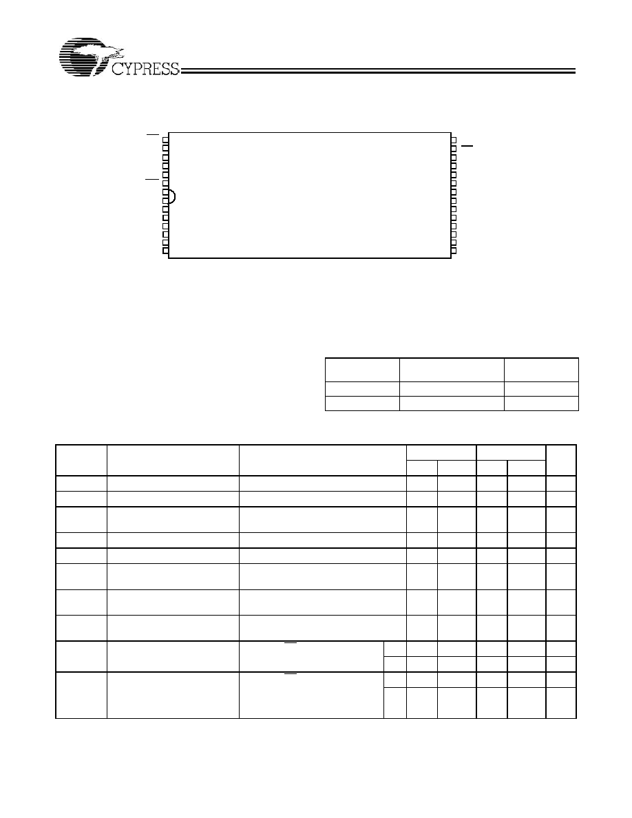
Pin Configuration
22
23
24
25
26
27
28
1
2
5
10
11
15
14
13
12
16
19
18
17
Top View
TSOP
3
4
20
21
7
6
8
9
OE
A
1
A
2
A
3
A
4
WE
V
CC
A
5
A
6
A
7
A
8
A
9
A
0
CE
I/O
7
I/O
6
I/O
5
GND
I/O
2
I/O
1
I/O
4
I/O
0
A
14
A
10
A
11
A
13
A
12
I/O
3
Operating Range
Range
Ambient
Temperature
V
CC
Commercial
0
°
C to +70
°
C
3.3V
±
300 mV
Industrial
40
°
C to +85
°
C
3.3V
±
300 mV
Electrical Characteristics
Over the Operating Range
[1]
7C1399B-10
7C1399B-12
Parameter
Description
Test Conditions
Min.
Max.
Min.
Max.
Unit
V
OH
Output HIGH Voltage
V
CC
= Min., I
OH
= 2.0 mA
2.4
2.4
V
V
OL
Output LOW Voltage
V
CC
= Min., I
OL
= 4.0 mA
0.4
0.4
V
V
IH
Input HIGH Voltage
2.2
V
CC
+0.3V
2.2
V
CC
+0.3V
V
V
IL
Input LOW Voltage
[2]
0.3
0.8
0.3
0.8
V
I
IX
Input Load Current
1
+1
1
+1
µ
A
I
OZ
Output Leakage
Current
GND
V
I
V
CC
,
Output Disabled
5
+5
5
+5
µ
A
I
OS
Output Short
Circuit Current
[3]
V
CC
= Max., V
OUT
= GND
300
300
mA
I
CC
V
CC
Operating
Supply Current
V
CC
= Max., I
OUT
= 0 mA,
f = f
MAX
= 1/t
RC
60
55
mA
I
SB1
Automatic CE Power-Down
Current -- TTL Inputs
Max. V
CC
, CE
V
IH
,
V
IN
V
IH
, or V
IN
V
IL
,f = f
MAX
5
5
mA
L
4
4
mA
I
SB2
Automatic CE Power-Down
Current -- CMOS Inputs
[4]
Max. V
CC
, CE
V
CC
0.3V, V
IN
V
CC
0.3V, or V
IN
0.3V,
WE
V
CC
0.3V or WE
0.3V,
f = f
MAX
500
500
µ
A
L
50
50
µ
A
Notes:
2.
Minimum voltage is equal to 2.0V for pulse durations of less than 20 ns.
3.
Not more than one output should be shorted at one time. Duration of the short circuit should not exceed 30 seconds.
4.
Device draws low standby current regardless of switching on the addresses.
CY7C1399B
Document #: 38-05071 Rev. *C
Page 3 of 10
Electrical Characteristics
Over the Operating Range (continued)
1399B-15
1399B-20
Parameter
Description
Test Conditions
Min.
Max.
Min.
Max.
Unit
V
OH
Output HIGH Voltage
V
CC
= Min., I
OH
= 2.0 mA
2.4
2.4
V
V
OL
Output LOW Voltage
V
CC
= Min., I
OL
= 4.0 mA
0.4
0.4
V
V
IH
Input HIGH Voltage
2.2
V
CC
+0.3V
2.2
V
CC
+0.3V
V
V
IL
Input LOW Voltage
0.3
0.8
0.3
0.8
V
I
IX
Input Load Current
1
+1
1
+1
µ
A
I
OZ
Output Leakage Current
GND
V
I
V
CC
,
Output Disabled
5
+5
5
+5
µ
A
I
OS
Output Short Circuit
Current
[3]
V
CC
= Max., V
OUT
= GND
300
300
mA
I
CC
V
CC
Operating
Supply Current
V
CC
= Max., I
OUT
= 0 mA,
f = f
MAX
= 1/t
RC
50
45
mA
I
SB1
Automatic CE Power-Down
Current -- TTL Inputs
Max. V
CC
, CE
V
IH
,
V
IN
V
IH
, or V
IN
V
IL
,
f = f
MAX
5
5
mA
L
4
4
mA
I
SB2
Automatic CE Power-Down
Current -- CMOS Inputs
[4]
Max. V
CC
, CE
V
CC
0.3V, V
IN
V
CC
0.3V, or V
IN
0.3V,
WE
V
CC
0.3V or WE
0.3V,
f=f
MAX
500
500
µ
A
L
50
50
µ
A
Capacitance
[5]
Parameter
Description
Test Conditions
Max.
Unit
C
IN
: Addresses
Input Capacitance
T
A
= 25
°
C, f = 1 MHz, V
CC
= 3.3V
5
pF
C
IN
: Controls
6
pF
C
OUT
Output Capacitance
6
pF
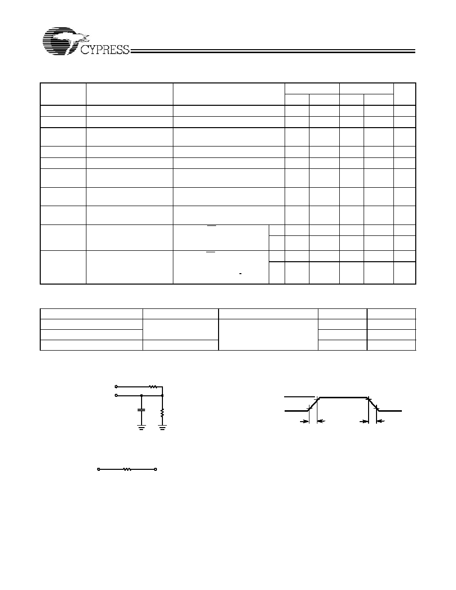
AC Test Loads and Waveforms
Note:
5.
Tested initially and after any design or process changes that may affect these parameters.
3.0V
3.3V
OUTPUT
R1 317
R2
351
C
L
INCLUDING
JIG AND
SCOPE
GND
90%
10%
90%
10%
3 ns
3 ns
OUTPUT
1.73V
Equivalent to:
THÉVENIN EQUIVALENT
ALL INPUT PULSES
167
CY7C1399B
Document #: 38-05071 Rev. *C
Page 4 of 10
Switching Characteristics
Over the Operating Range
[6]
1399B-10
1399B-12
Parameter
Description
Min.
Max.
Min.
Max.
Unit
Read Cycle
t
RC
Read Cycle Time
10
12
ns
t
AA
Address to Data Valid
10
12
ns
t
OHA
Data Hold from Address Change
3
3
ns
t
ACE
CE LOW to Data Valid
10
12
ns
t
DOE
OE LOW to Data Valid
5
5
ns
t
LZOE
OE LOW to Low Z
[7]
0
0
ns
t
HZOE
OE HIGH to High Z
[7, 8]
5
5
ns
t
LZCE
CE LOW to Low Z
[7]
3
3
ns
t
HZCE
CE HIGH to High Z
[7, 8]
5
6
ns
t
PU
CE LOW to Power-Up
0
0
ns
t
PD
CE HIGH to Power-Down
10
12
ns
Write Cycle
[9, 10]
t
WC
Write Cycle Time
10
12
ns
t
SCE
CE LOW to Write End
8
8
ns
t
AW
Address Set-Up to Write End
7
8
ns
t
HA
Address Hold from Write End
0
0
ns
t
SA
Address Set-Up to Write Start
0
0
ns
t
PWE
WE Pulse Width
7
8
ns
t
SD
Data Set-Up to Write End
5
7
ns
t
HD
Data Hold from Write End
0
0
ns
t
HZWE
WE LOW to High Z
[9]
7
7
ns
t
LZWE
WE HIGH to Low Z
[7]
3
3
ns
Notes:
6.
Test conditions assume signal transition time of 3 ns or less, timing reference levels of 1.5V, input pulse levels of 0 to 3.0V, and output loading of the specified
I
OL
/I
OH
and capacitance C
L
= 30 pF.
7.
At any given temperature and voltage condition, t
HZCE
is less than t
LZCE
, t
HZOE
is less than t
LZOE
, and t
HZWE
is less than t
LZWE
for any given device.
8.
t
HZOE
, t
HZCE
, t
HZWE
are specified with C
L
= 5 pF as in AC Test Loads. Transition is measured ±500 mV from steady state voltage.
9.
The internal write time of the memory is defined by the overlap of CE LOW and WE LOW. Both signals must be LOW to initiate a write and either signal can terminate
a write by going HIGH. The data input set-up and hold timing should be referenced to the rising edge of the signal that terminates the write.
10. The minimum write cycle time for write cycle #3 (WE controlled, OE LOW) is the sum of t
HZWE
and t
SD
.
CY7C1399B
Document #: 38-05071 Rev. *C
Page 5 of 10
Switching Characteristics
Over the Operating Range
[6]
(Continued)
1399B-15
1399B-20
Parameter
Description
Min.
Max.
Min.
Max.
Unit
Read Cycle
t
RC
Read Cycle Time
15
20
ns
t
AA
Address to Data Valid
15
20
ns
t
OHA
Data Hold from Address Change
3
3
ns
t
ACE
CE LOW to Data Valid
15
20
ns
t
DOE
OE LOW to Data Valid
6
7
ns
t
LZOE
OE LOW to Low Z
[7]
0
0
ns
t
HZOE
OE HIGH to High Z
[7, 8]
6
6
ns
t
LZCE
CE LOW to Low Z
[7]
3
3
ns
t
HZCE
CE HIGH to High Z
[7, 8]
7
7
ns
t
PU
CE LOW to Power-Up
0
0
ns
t
PD
CE HIGH to Power-Down
15
20
ns
Write Cycle
[9, 10]
t
WC
Write Cycle Time
15
20
ns
t
SCE
CE LOW to Write End
10
12
ns
t
AW
Address Set-Up to Write End
10
12
ns
t
HA
Address Hold from Write End
0
0
ns
t
SA
Address Set-Up to Write Start
0
0
ns
t
PWE
WE Pulse Width
10
12
ns
t
SD
Data Set-Up to Write End
8
10
ns
t
HD
Data Hold from Write End
0
0
ns
t
HZWE
WE LOW to High Z
[9]
7
7
ns
t
LZWE
WE HIGH to Low Z
[7]
3
3
ns
Data Retention Characteristics
(Over the Operating Range - L version only)
Parameter
Description
Conditions
Min.
Max.
Unit
V
DR
V
CC
for Data Retention
2.0
V
I
CCDR
Data Retention Current
Com'l
V
CC
= V
DR
= 2.0V,
CE > V
CC
0.3V,
V
IN
> V
CC
0.3V or
V
IN
< 0.3V
0
20
µ
A
t
CDR
Chip Deselect to Data
Retention Time
0
ns
t
R
Operation Recovery Time
t
RC
ns
CY7C1399B
Document #: 38-05071 Rev. *C
Page 6 of 10
Data Retention Waveform
3.0V
3.0V
t
CDR
V
DR
>
2V
DATA RETENTION MODE
t
R
CE
V
CC
Switching Waveforms
Notes:
11. Device is continuously selected. OE, CE = V
IL
.
12. WE is HIGH for read cycle.
13. Address valid prior to or coincident with CE transition LOW.
ADDRESS
DATA OUT
PREVIOUS DATA VALID
DATA VALID
t
RC
t
AA
t
OHA
Read Cycle No. 1
[11, 12]
50%
50%
DATA VALID
t
RC
t
ACE
t
DOE
t
LZOE
t
LZCE
t
PU
DATA OUT
HIGH IMPEDANCE
IMPEDANCE
ICC
ISB
t
HZOE
t
HZCE
t
PD
OE
CE
HIGH
V
CC
SUPPLY
CURRENT
Read Cycle No. 2
[12, 13]
CY7C1399B
Document #: 38-05071 Rev. *C
Page 7 of 10
Notes:
14. Data I/O is high impedance if OE = V
IH
.
15. If CE goes HIGH simultaneously with WE HIGH, the output remains in a high-impedance state.
16. During this period, the I/Os are in the output state and input signals should not be applied.
Switching Waveforms
(continued)
t
HD
t
SD
t
PWE
t
SA
t
HA
t
AW
t
WC
DATA I/O
ADDRESS
CE
WE
OE
t
HZOE
DATA
IN
VALID
Write Cycle No. 1 (WE Controlled)
[9, 14, 15]
NOTE 16
t
WC
t
AW
t
SA
t
HA
t
HD
t
SD
t
SCE
WE
DATA I/O
ADDRESS
CE
DATA
IN
VALID
Write Cycle No. 2 (CE Controlled)
[9, 14, 15]
DATA I/O
ADDRESS
t
HD
t
SD
t
LZWE
t
SA
t
HA
t
AW
t
WC
CE
WE
t
HZWE
DATA
IN
VALID
Write Cycle No. 3 (WE Controlled, OE LOW)
[10, 15]
NOTE 16
CY7C1399B
Document #: 38-05071 Rev. *C
Page 8 of 10
l product and comany names mentioned in this document may be the trademarks of their respective holders.
Truth Table
CE
WE
OE
Input/Output
Mode
Power
H
X
X
High Z
Deselect/Power-Down
Standby (I
SB
)
L
H
L
Data Out
Read
Active (I
CC
)
L
L
X
Data In
Write
Active (I
CC
)
L
H
H
High Z
Deselect, Output Disabled
Active (I
CC
)
Ordering Information
Speed
(ns)
Ordering Code
Package
Name
Package Type
Operating
Range
10
CY7C1399B-10VC
V21
28-Lead Molded SOJ
Commercial
CY7C1399B-10ZC
Z28
28-Lead Thin Small Outline Package
CY7C1399BL-10VC
V21
28-Lead Molded SOJ
CY7C1399BL-10ZC
Z28
28-Lead Thin Small Outline Package
12
CY7C1399B-12VC
V21
28-Lead Molded SOJ
CY7C1399B-12ZC
Z28
28-Lead Thin Small Outline Package
CY7C1399BL-12VC
V21
28-Lead Molded SOJ
CY7C1399BL-12ZC
Z28
28-Lead Thin Small Outline Package
CY7C1399B-12VI
V21
28-Lead Molded SOJ
Industrial
CY7C1399B-12ZI
Z28
28-Lead Thin Small Outline Package
15
CY7C1399B-15VC
V21
28-Lead Molded SOJ
Commercial
CY7C1399B-15ZC
Z28
28-Lead Thin Small Outline Package
CY7C1399BL-15VC
V21
28-Lead Molded SOJ
CY7C1399BL-15ZC
Z28
28-Lead Thin Small Outline Package
CY7C1399B-15VI
V21
28-Lead Molded SOJ
Industrial
CY7C1399B-15ZI
Z28
28-Lead Thin Small Outline Package
20
CY7C1399B-20VC
V21
28-Lead Molded SOJ
Commercial
CY7C1399B-20ZC
Z28
28-Lead Thin Small Outline Package
CY7C1399BL-20VC
V21
28-Lead Molded SOJ
CY7C1399BL-20ZC
Z28
28-Lead Thin Small Outline Package
CY7C1399B-20VI
V21
28-Lead Molded SOJ
Industrial
CY7C1399B-20ZI
Z28
28-Lead Thin Small Outline Package
CY7C1399B
Document #: 38-05071 Rev. *C
Page 9 of 10
© Cypress Semiconductor Corporation, 2001. The information contained herein is subject to change without notice. Cypress Semiconductor Corporation assumes no responsibility for the use
of any circuitry other than circuitry embodied in a Cypress Semiconductor product. Nor does it convey or imply any license under patent or other rights. Cypress Semiconductor does not authorize
its products for use as critical components in life-support systems where a malfunction or failure may reasonably be expected to result in significant injury to the user. The inclusion of Cypress
Semiconductor products in life-support systems application implies that the manufacturer assumes all risk of such use and in doing so indemnifies Cypress Semiconductor against all charges.
Package Diagrams
28-Lead (300-Mil) Molded SOJ V21
51-85031-B
28-Lead Thin Small Outline Package Type 1 (8x13.4 mm) Z28
51-85071-*G
CY7C1399B
Document #: 38-05071 Rev. *C
Page 10 of 10
Document History Page
Document Title: CY7C1399B 32K x 8 3.3V Static RAM
Document Number: 38-05071
REV.
ECN NO.
ISSUE
DATE
ORIG. OF
CHANGE
DESCRIPTION OF CHANGE
**
107264
05/25/01
SZV
Change from Spec #: 38-01102 to 38-05071
*A
107533
06/28/01
MAX
Add Low Power
*B
116472
09/17/02
CEA
Add applications foot note to data sheet, page 1.
*C
224340
See ECN
RKF
Option 1 of the Orientation ID on TSOP-I Package Diagram [Page #9]
removed