PRELIMINARY
36-Mbit QDR-IITM SRAM 2-Word
Burst Architecture
CY7C1410AV18
CY7C1425AV18
CY7C1412AV18
CY7C1414AV18
Cypress Semiconductor Corporation
∑
3901 North First Street
∑
San Jose
,
CA 95134
∑
408-943-2600
Document #: 38-05615 Rev. **
Revised July 06, 2004
Features
∑ Separate Independent Read and Write data ports
-- Supports concurrent transactions
∑ 200-MHz clock for high bandwidth
∑ 2-Word Burst on all accesses
∑ Double Data Rate (DDR) interfaces on both Read and
Write ports (data transferred at 400 MHz) @ 200 MHz
∑ Two input clocks (K and K) for precise DDR timing
-- SRAM uses rising edges only
∑ Two output clocks (C and C) accounts for clock skew
and flight time mismatching
∑ Echo clocks (CQ and CQ) simplify data capture in
high-speed systems
∑ Single multiplexed address input bus latches address
inputs for both Read and Write ports
∑ Separate Port Selects for depth expansion
∑ Synchronous internally self-timed writes
∑ Available in x8, x9, x18, and x36 configurations
∑ Full data coherency, providing most current data
∑ Core V
DD
= 1.8V (±0.1V); I/O V
DDQ
= 1.4V to V
DD
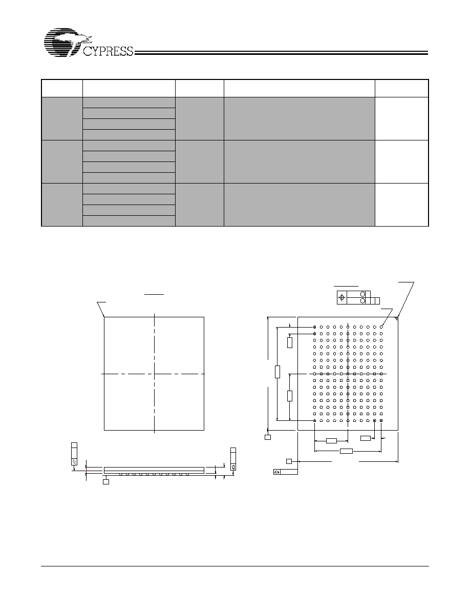
∑ 15 ◊ 17 ◊ 1.4 mm 1.0-mm pitch FBGA package, 165-ball
(11 ◊ 15 matrix)
∑ Variable drive HSTL output buffers
∑ JTAG 1149.1 compatible test access port
∑ Delay Lock Loop (DLL) for accurate data placement
Configurations
CY7C1410AV18 ≠ 4M x 8
CY7C1425AV18 ≠ 4M x 9
CY7C1412AV18 ≠ 2M x 18
CY7C1414AV18 ≠ 1M x 36
Functional Description
The CY7C1410AV18, CY7C1425AV18, CY7C1412AV18, and
CY7C1414AV18 are 1.8V Synchronous Pipelined SRAMs,
equipped with QDRTM-II architecture. QDR-II architecture
consists of two separate ports to access the memory array.
The Read port has dedicated Data Outputs to support Read
operations and the Write Port has dedicated Data Inputs to
support Write operations. QDR-II architecture has separate
data inputs and data outputs to completely eliminate the need
to "turn-around" the data bus required with common I/O
devices. Access to each port is accomplished through a
common address bus. The Read address is latched on the
rising edge of the K clock and the Write address is latched on
the rising edge of the K clock. Accesses to the QDR-II Read
and Write ports are completely independent of one another. In
order to maximize data throughput, both Read and Write ports
are equipped with Double Data Rate (DDR) interfaces. Each
address location is associated with two 8-bit words
(CY7C1410AV18) or 9-bit words (CY7C1425AV18) or 18-bit
words (CY7C1412AV18) or 36-bit words (CY7C1414AV18)
that burst sequentially into or out of the device. Since data can
be transferred into and out of the device on every rising edge
of both input clocks (K and K and C and C), memory bandwidth
is maximized while simplifying system design by eliminating
bus "turn-arounds."
Depth expansion is accomplished with Port Selects for each
port. Port selects allow each port to operate independently.
All synchronous inputs pass through input registers controlled
by the K or K input clocks. All data outputs pass through output
registers controlled by the C or C (or K or K in a single clock
domain) input clocks. Writes are conducted with on-chip
synchronous self-timed write circuitry.
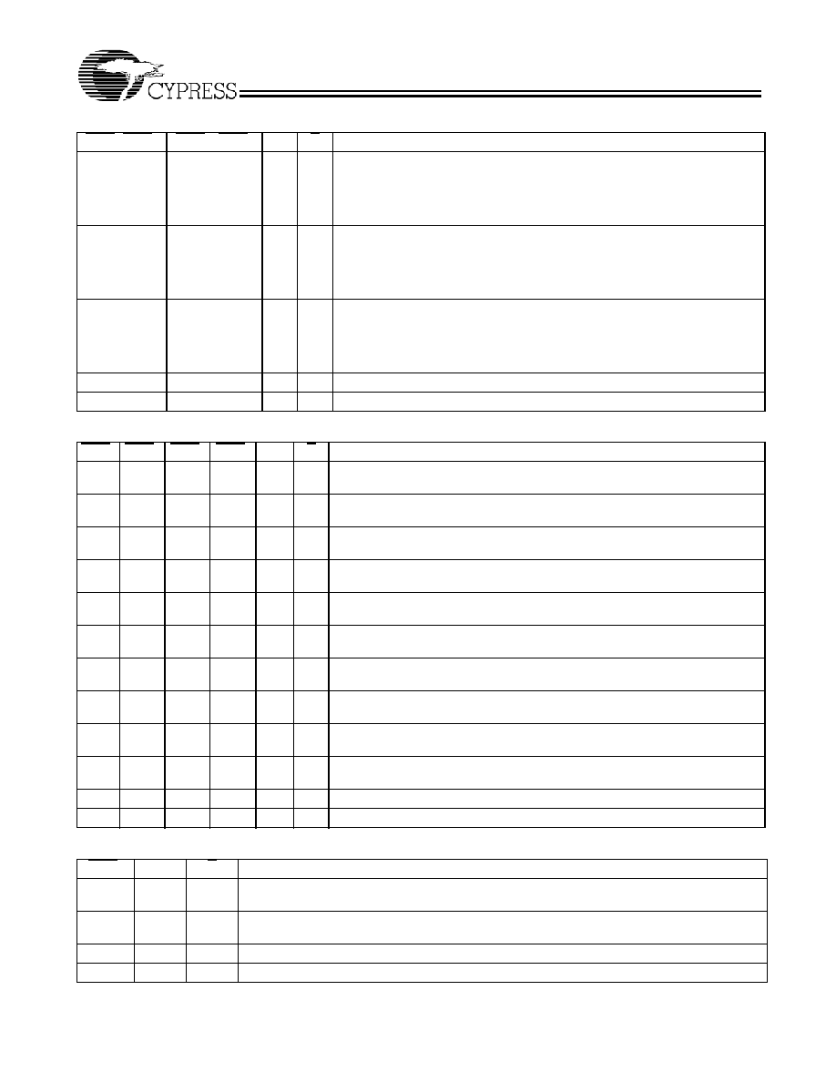
Selection Guide
250 MHz
200 MHz
167 MHz
Unit
Maximum Operating Frequency
250
200
167
MHz
Maximum Operating Current
TBD
TBD
TBD
mA
Shaded areas contain advance information.
Please contact your local Cypress Sales representative for availability of these parts.
PRELIMINARY
CY7C1410AV18
CY7C1425AV18
CY7C1412AV18
CY7C1414AV18
Document #: 38-05615 Rev. **
Page 2 of 23
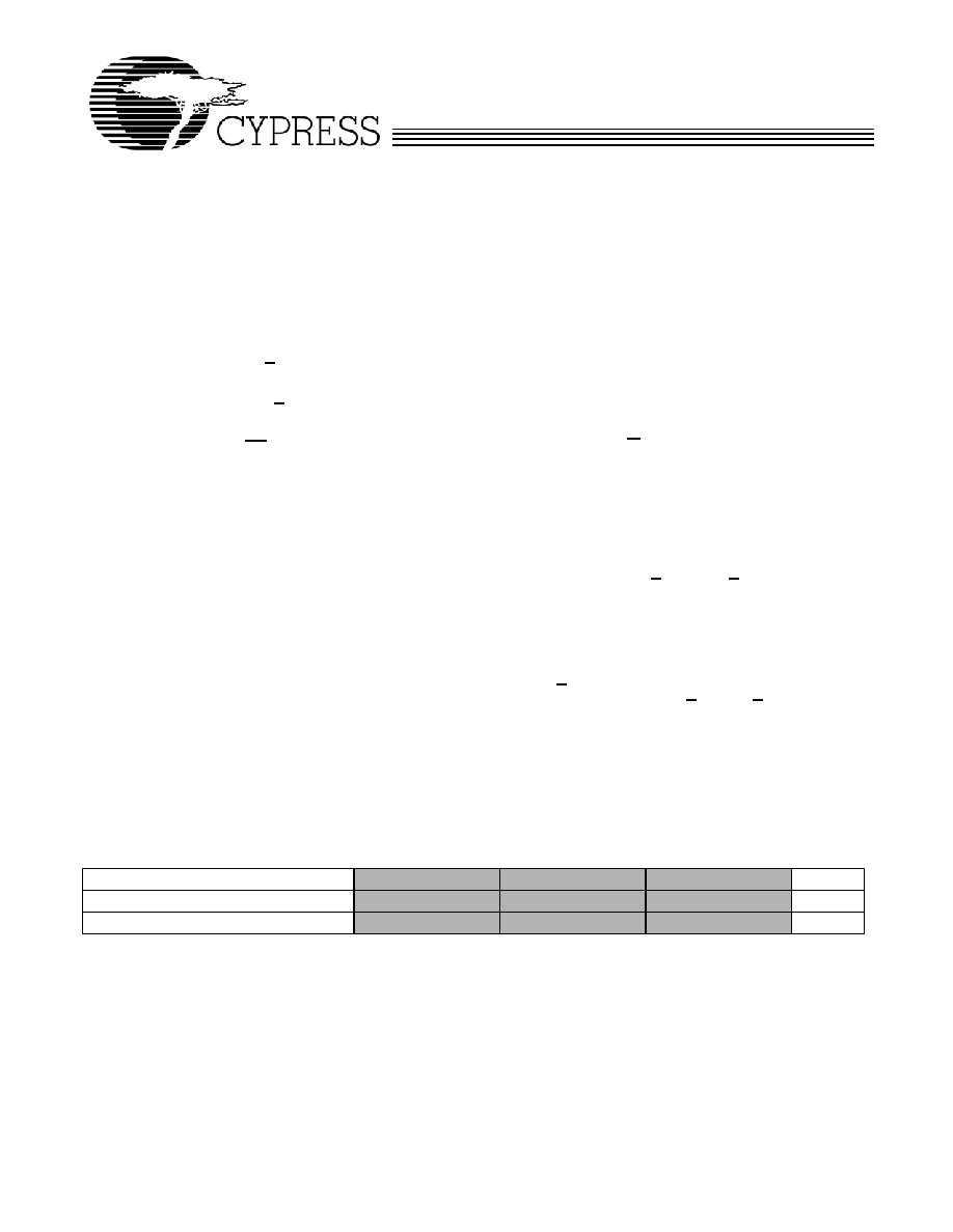
Logic Block Diagram (CY7C1410AV18)
CLK
A
(20:0)
Gen.
K
K
Control
Logic
Address
Register
D
[7:0]
Re
ad
Ad
d. D
e
c
o
d
e
Read Data Reg.
RPS
WPS
Q
[7:0]
Control
Logic
Address
Register
Reg.
Reg.
Reg.
8
21
8
16
8
NWS
[1:0]
V
REF
W
r
i
t
e
Ad
d.
Dec
ode
8
A
(20:0)
21
C
C
8
2M x 8 Ar
r
a
y
2M
x 8 Ar
r
a
y
Write
Reg
Write
Reg
CQ
CQ
8
DOFF
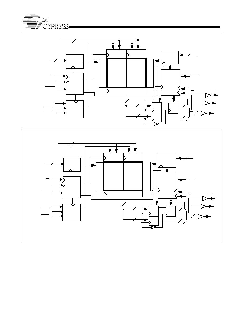
Logic Block Diagram (CY7C1425AV18)
CLK
A
(20:0)
Gen.
K
K
Control
Logic
Address
Register
D
[8:0]
Re
ad
Ad
d.
Dec
o
d
e
Read Data Reg.
RPS
WPS
Q
[8:0]
Control
Logic
Address
Register
Reg.
Reg.
Reg.
9
21
9
18
9
BWS
[0]
V
REF
W
r
i
t
e A
d
d
.
Deco
de
9
A
(20:0)
21
C
C
9
2
M
x 9 Arra
y
2
M
x 9 Arra
y
Write
Reg
Write
Reg
CQ
CQ
9
DOFF
PRELIMINARY
CY7C1410AV18
CY7C1425AV18
CY7C1412AV18
CY7C1414AV18
Document #: 38-05615 Rev. **
Page 3 of 23
Logic Block Diagram (CY7C1412AV18)
CLK
A
(19:0)
Gen.
K
K
Control
Logic
Address
Register
D
[17:0]
Re
ad
Ad
d
.
D
e
c
o
de
Read Data Reg.
RPS
WPS
Q
[17:0]
Control
Logic
Address
Register
Reg.
Reg.
Reg.
18
20
18
36
18
BWS
[1:0]
V
REF
W
r
i
t
e Ad
d.
Dec
ode
18
A
(19:0)
20
C
C
18
1M
x 18
Ar
r
a
y
1M x 18
Ar
r
a
y
Write
Reg
Write
Reg
CQ
CQ
18
DOFF
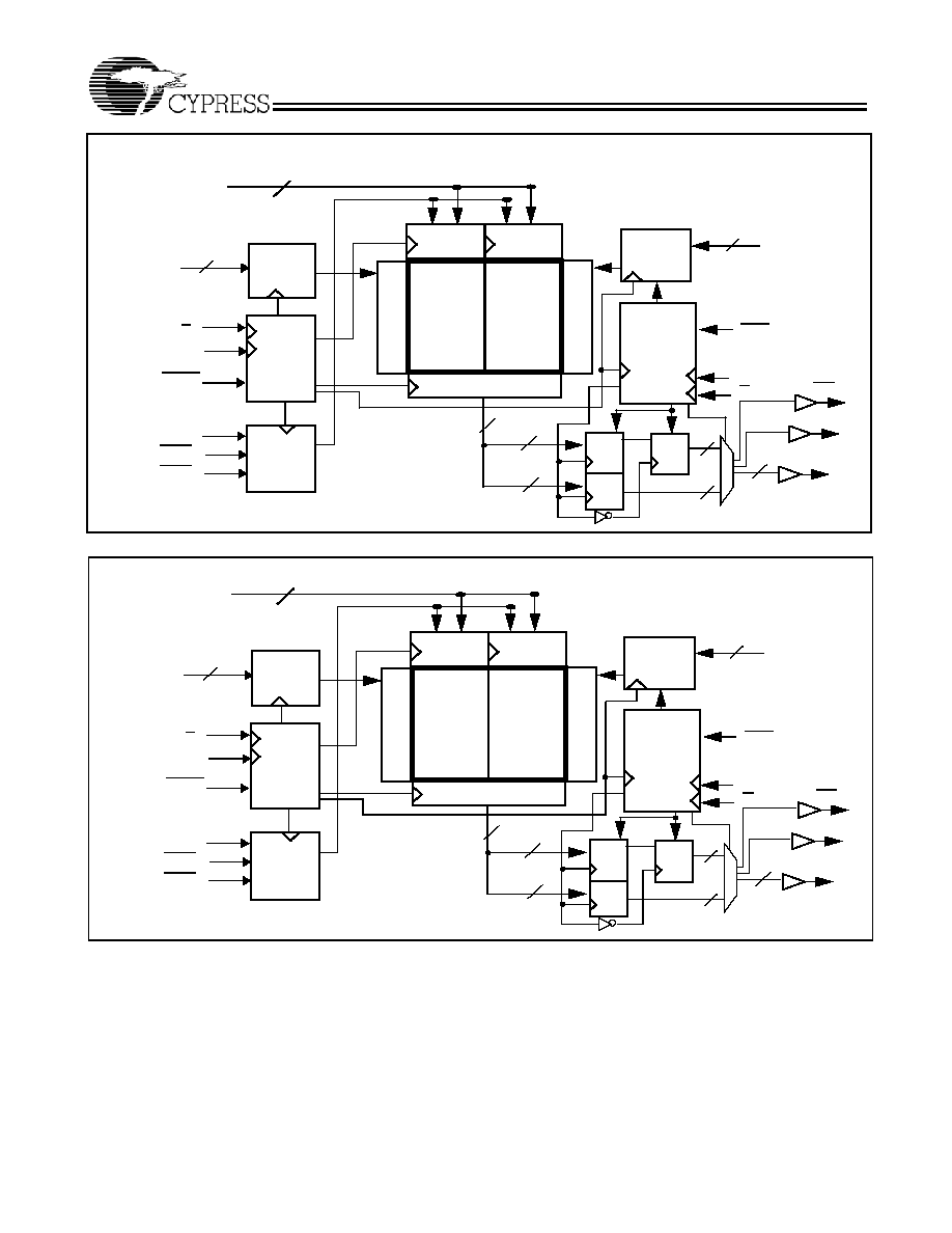
Logic Block Diagram (CY7C1414AV18)
CLK
A
(18:0)
Gen.
K
K
Control
Logic
Address
Register
D
[35:0]
R
e
ad
Ad
d. De
c
o
d
e
Read Data Reg.
RPS
WPS
Q
[35:0]
Control
Logic
Address
Register
Reg.
Reg.
Reg.
36
19
36
72
36
BWS
[3:0]
V
REF
W
r
ite A
d
d
.
D
e
c
o
de
36
A
(18:0)
19
C
C
36
512K x 36 Ar
ra
y
512K x
3
6
Arr
a
y
Write
Reg
Write
Reg
CQ
CQ
36
DOFF
PRELIMINARY
CY7C1410AV18
CY7C1425AV18
CY7C1412AV18
CY7C1414AV18
Document #: 38-05615 Rev. **
Page 4 of 23
Pin Configurations
CY7C1410AV18 (4M ◊ 8) ≠ 15 ◊ 17 FBGA
2
3
4
5
6
7
1
A
B
C
D
E
F
G
H
J
K
L
M
N
P
R
A
CQ
NC
NC
NC
NC
DOFF
NC
NC/72M
A
NWS
1
K
WPS
NC/144M
NC
NC
NC
NC
NC
TDO
NC
NC
D5
NC
NC
NC
TCK
NC
NC
A NC/288M
K
NWS
0
V
SS
A
A
A
NC
V
SS
V
SS
V
SS
V
SS
V
DD
A
V
SS
V
SS
V
SS
V
DD
Q4
NC
V
DDQ
NC
NC
NC
NC
Q7
A
V
DDQ
V
SS
V
DDQ
V
DD
V
DD
Q5
V
DDQ
V
DD
V
DDQ
V
DD
V
DDQ
V
DD
V
SS
V
DD
V
DDQ
V
DDQ
V
SS
V
SS
V
SS
V
SS
A
A
C
V
SS
A
A
A
D4
V
SS
NC
V
SS
NC
NC
V
REF
V
SS
V
DD
V
SS
V
SS
A
V
SS
C
NC
Q6
NC
D7
D6
V
DD
A
8
9
10
11
NC
A
A
RPS
CQ
A NC
NC
Q3
V
SS
NC
NC
D3
NC
V
SS
NC
Q2
NC
NC
NC
V
REF
NC
NC
V
DDQ
NC
V
DDQ
NC
NC
V
DDQ
V
DDQ
V
DDQ
D1
V
DDQ
NC
Q1
NC
V
DDQ
V
DDQ
NC
V
SS
NC
D0
NC
TDI
TMS
V
SS
A
NC
A
NC
D2
NC
ZQ
NC
Q0
NC
NC
NC
NC
A
CY7C1425AV18 (4M ◊ 9)≠11 ◊ 15 Balls (15 ◊ 17 FBGA)
2
3
4
5
6
7
1
A
B
C
D
E
F
G
H
J
K
L
M
N
P
R
A
CQ
NC
NC
NC
NC
DOFF
NC
NC/72M
A
NC
K
WPS
NC/144M
NC
NC
NC
NC
NC
TDO
NC
NC
D6
NC
NC
NC
TCK
NC
NC
A NC/288M
K
BWS
0
V
SS
A
A
A
NC
V
SS
V
SS
V
SS
V
SS
V
DD
A
V
SS
V
SS
V
SS
V
DD
Q5
NC
V
DDQ
NC
NC
NC
NC
Q8
A
V
DDQ
V
SS
V
DDQ
V
DD
V
DD
Q6
V
DDQ
V
DD
V
DDQ
V
DD
V
DDQ
V
DD
V
SS
V
DD
V
DDQ
V
DDQ
V
SS
V
SS
V
SS
V
SS
A
A
C
V
SS
A
A
A
D5
V
SS
NC
V
SS
NC
NC
V
REF
V
SS
V
DD
V
SS
V
SS
A
V
SS
C
NC
Q7
NC
D8
D7
V
DD
A
8
9
10
11
Q0
A
A
RPS
CQ
A NC
NC
Q4
V
SS
NC
NC
D4
NC
V
SS
NC
Q3
NC
NC
NC
V
REF
NC
NC
V
DDQ
NC
V
DDQ
NC
NC
V
DDQ
V
DDQ
V
DDQ
D2
V
DDQ
NC
Q2
NC
V
DDQ
V
DDQ
NC
V
SS
NC
D1
NC
TDI
TMS
V
SS
A
NC
A
NC
D3
NC
ZQ
NC
Q1
NC
NC
D0
NC
A
PRELIMINARY
CY7C1410AV18
CY7C1425AV18
CY7C1412AV18
CY7C1414AV18
Document #: 38-05615 Rev. **
Page 5 of 23
Pin Configurations
(continued)
CY7C1412AV18 (2M ◊ 18) ≠ 15 ◊ 17 FBGA
2
3
4
5
6
7
1
A
B
C
D
E
F
G
H
J
K
L
M
N
P
R
A
CQ
NC
NC
NC
NC
DOFF
NC
NC/144M
A
BWS
1
K
WPS
NC/288M
Q9
D9
NC
NC
NC
TDO
NC
NC
D13
NC
NC
NC
TCK
NC
D10
A NC
K
BWS
0
V
SS
A
A
A
Q10
V
SS
V
SS
V
SS
V
SS
V
DD
A
V
SS
V
SS
V
SS
V
DD
Q11
D12
V
DDQ
D14
Q14
D16
Q16
Q17
A
V
DDQ
V
SS
V
DDQ
V
DD
V
DD
Q13
V
DDQ
V
DD
V
DDQ
V
DD
V
DDQ
V
DD
V
SS
V
DD
V
DDQ
V
DDQ
V
SS
V
SS
V
SS
V
SS
A
A
C
V
SS
A
A
A
D11
V
SS
NC
V
SS
Q12
NC
V
REF
V
SS
V
DD
V
SS
V
SS
A
V
SS
C
NC
Q15
NC
D17
D15
V
DD
A
8
9
10
11
Q0
A
NC/72M
RPS
CQ
A NC
NC
Q8
V
SS
NC
Q7
D8
NC
V
SS
NC
Q6
D5
NC
NC
V
REF
NC
Q3
V
DDQ
NC
V
DDQ
NC
Q5
V
DDQ
V
DDQ
V
DDQ
D4
V
DDQ
NC
Q4
NC
V
DDQ
V
DDQ
NC
V
SS
NC
D2
NC
TDI
TMS
V
SS
A
NC
A
D7
D6
NC
ZQ
D3
Q2
D1
Q1
D0
NC
A
2
3
4
5
6
7
1
A
B
C
D
E
F
G
H
J
K
L
M
N
P
R
A
CQ
Q27
D27
D28
D34
DOFF
Q33
NC/288M NC/72M
BWS
2
K
WPS
BWS
1
Q18
D18
Q30
D31
D33
TDO
Q28
D29
D22
D32
Q34
Q31
TCK
D35
D19
A
BWS
3
K
BWS
0
V
SS
A
A
A
Q19
V
SS
V
SS
V
SS
V
SS
V
DD
A
V
SS
V
SS
V
SS
V
DD
Q20
D21
V
DDQ
D23
Q23
D25
Q25
Q26
A
V
DDQ
V
SS
V
DDQ
V
DD
V
DD
Q22
V
DDQ
V
DD
V
DDQ
V
DD
V
DDQ
V
DD
V
SS
V
DD
V
DDQ
V
DDQ
V
SS
V
SS
V
SS
V
SS
A
A
C
V
SS
A
A
A
D20
V
SS
Q29
V
SS
Q21
D30
V
REF
V
SS
V
DD
V
SS
V
SS
A
V
SS
C
Q32
Q24
Q35
D26
D24
V
DD
A
8
9
10
11
Q0
A
NC/144M
RPS
CQ
A D17
Q17
Q8
V
SS
D16
Q7
D8
Q16
V
SS
D15
Q6
D5
D9
Q14
V
REF
Q11
Q3
V
DDQ
Q15
V
DDQ
D14
Q5
V
DDQ
VDDQ
V
DDQ
D4
V
DDQ
D12
Q4
Q12
V
DDQ
V
DDQ
D11
V
SS
D10
D2
Q10
TDI
TMS
V
SS
A
Q9
A
D7
D6
D13
ZQ
D3
Q2
D1
Q1
D0
Q13
A
CY7C1414AV18 (1M ◊ 36) ≠ 15 ◊ 17 FBGA
PRELIMINARY
CY7C1410AV18
CY7C1425AV18
CY7C1412AV18
CY7C1414AV18
Document #: 38-05615 Rev. **
Page 6 of 23
Pin Definitions
Pin Name
I/O
Pin Description
D
[x:0]
Input-
Synchronous
Data input signals, sampled on the rising edge of K and K clocks during valid write
operations.
CY7C1410AV18 - D
[7:0]
CY7C1425AV18 - D
[8:0]
CY7C1412AV18 - D
[17:0]
CY7C1414AV18 - D
[35:0]
WPS
Input-
Synchronous
Write Port Select, active LOW. Sampled on the rising edge of the K clock. When
asserted active, a Write operation is initiated. Deasserting will deselect the Write port.
Deselecting the Write port will cause D
[x:0]
to be ignored.
NWS
0,
NWS
1
Nibble Write Select 0, 1
-
active LOW. (CY7C1410AV18 Only) Sampled on the rising
edge of the K and K clocks during Write operations. Used to select which nibble is written
into the device during the current portion of the Write operations.Nibbles not written
remain unaltered. NWS
0
controls D
[3:0]
and NWS
1
controls D
[7:4]
. All Nibble Write Selects
are sampled on the same edge as the data. Deselecting a Nibble Write Select will cause
the corresponding nibble of data to be ignored and not written into the device.
BWS
0
, BWS
1
,
BWS
2
, BWS
3
Input-
Synchronous
Byte Write Select 0, 1, 2 and 3
-
active LOW. Sampled on the rising edge of the K and
K clocks during Write operations. Used to select which byte is written into the device
during the current portion of the Write operations. Bytes not written remain unaltered.
CY7C1425AV18
-
BWS
0
controls D
[8:0]
CY7C1412AV18
-
BWS
0
controls D
[8:0]
, BWS
1
controls D
[17:9]
.
CY7C1414AV18
-
BWS
0
controls D
[8:0]
, BWS
1
controls D
[17:9]
,BWS
2
controls D
[26:18]
and BWS
3
controls D
[35:27].
All the Byte Write Selects are sampled on the same edge as the data. Deselecting a Byte
Write Select will cause the corresponding byte of data to be ignored and not written into
the device.
A
Input-
Synchronous
Address Inputs. Sampled on the rising edge of the K (Read address) and K (Write
address) clocks during active Read and Write operations. These address inputs are
multiplexed for both Read and Write operations. Internally, the device is organized as 4M
x 8 (2 arrays each of 2M x 8) for CY7C1410AV18, 4M x 9 (2 arrays each of 2M x 9) for
CY7C1425AV18, 2M x 18 (2 arrays each of 1M x 18) for CY7C1412AV18 and 1M x 36
(2 arrays each of 512K x 36) for CY7C1414AV18. Therefore, only 21 address inputs are
needed to access the entire memory array of CY7C1410AV18 and CY7C1425AV18, 20
address inputs for CY7C1412AV18 and 19 address inputs for CY7C1414AV18. These
inputs are ignored when the appropriate port is deselected.
Q
[x:0]
Outputs-
Synchronous
Data Output signals. These pins drive out the requested data during a Read operation.
Valid data is driven out on the rising edge of both the C and C clocks during Read
operations or K and K when in single clock mode. When the Read port is deselected,
Q
[x:0]
are automatically three-stated.
CY7C1410AV18
-
Q
[7:0]
CY7C1425AV18
-
Q
[8:0]
CY7C1412AV18
-
Q
[17:0]
CY7C1414AV18
-
Q
[35:0]
RPS
Input-
Synchronous
Read Port Select, active LOW. Sampled on the rising edge of Positive Input Clock (K).
When active, a Read operation is initiated. Deasserting will cause the Read port to be
deselected. When deselected, the pending access is allowed to complete and the output
drivers are automatically three-stated following the next rising edge of the C clock. Each
read access consists of a burst of two sequential transfers.
C
Input-
Clock
Positive Output Clock Input. C is used in conjunction with C to clock out the Read data
from the device. C and C can be used together to deskew the flight times of various
devices on the board back to the controller. See application example for further details.
C
Input-Clock
Negative Output Clock Input. C is used in conjunction with C to clock out the Read data
from the device. C and C can be used together to deskew the flight times of various
devices on the board back to the controller. See application example for further details.
K
Input-Clock
Positive Input Clock Input. The rising edge of K is used to capture synchronous inputs
to the device and to drive out data through Q
[x:0]
when in single clock mode. All accesses
are initiated on the rising edge of K.
PRELIMINARY
CY7C1410AV18
CY7C1425AV18
CY7C1412AV18
CY7C1414AV18
Document #: 38-05615 Rev. **
Page 7 of 23
Functional Overview
The CY7C1410AV18, CY7C1425AV18, CY7C1412AV18 and
CY7C1414AV18 are synchronous pipelined Burst SRAMs
equipped with both a Read port and a Write port. The Read
port is dedicated to Read operations and the Write port is
dedicated to Write operations. Data flows into the SRAM
through the Write port and out through the Read port. These
devices multiplex the address inputs in order to minimize the
number of address pins required. By having separate Read
and Write ports, the QDR-II completely eliminates the need to
"turn-around" the data bus and avoids any possible data
contention, thereby simplifying system design. Each access
consists of two 8-bit data transfers in the case of
CY7C1410AV18, two 9-bit data transfers in the case of
CY7C1425AV18,two 18-bit data transfers in the case of
CY7C1412AV18 and two 36-bit data transfers in the case of
CY7C1414AV18, in one clock cycle.
Accesses for both ports are initiated on the rising edge of the
positive Input Clock (K). All synchronous input timings are
referenced from the rising edge of the input clocks (K and K)
and all output timings are referenced to the rising edge of
output clocks (C and C or K and K when in single clock mode).
All synchronous data inputs (D
[x:0]
) inputs pass through input
registers controlled by the input clocks (K and K). All
synchronous data outputs (Q
[x:0]
) outputs pass through output
registers controlled by the rising edge of the output clocks (C
and C or K and K when in single clock mode).
All synchronous control (RPS, WPS, BWS
[x:0]
) inputs pass
through input registers controlled by the rising edge of the
input clocks (K and K).
CY7C1412AV18 is described in the following sections. The
same basic descriptions apply to CY7C1410AV18
CY7C1425AV18 and CY7C1414AV18.
Read Operations
The CY7C1412AV18 is organized internally as 2 arrays of
1Mx18. Accesses are completed in a burst of two sequential
18-bit data words. Read operations are initiated by asserting
RPS
active at the rising edge of the Positive Input Clock (K).
The address is latched on the rising edge of the K Clock. The
address presented to Address inputs is stored in the Read
K
Input-Clock
Negative Input Clock Input. K is used to capture synchronous inputs being presented
to the device and to drive out data through Q
[x:0]
when in single clock mode.
CQ
Echo Clock
CQ is referenced with respect to C. This is a free running clock and is synchronized
to the output clock (C) of the QDR-II. In the single clock mode, CQ is generated with
respect to K. The timings for the echo clocks are shown in the AC Timing table.
CQ
Echo Clock
CQ is referenced with respect to C. This is a free running clock and is synchronized
to the output clock (C) of the QDR-II. In the single clock mode, CQ is generated with
respect to K. The timings for the echo clocks are shown in the AC Timing table.
ZQ
Input
Output Impedance Matching Input. This input is used to tune the device outputs to the
system data bus impedance. CQ, CQ, and Q
[x:0]
output impedance are set to 0.2 x RQ,
where RQ is a resistor connected between ZQ and ground. Alternately, this pin can be
connected directly to V
DD
, which enables the minimum impedance mode. This pin cannot
be connected directly to GND or left unconnected.
DOFF
Input
DLL Turn Off, active LOW. Connecting this pin to ground will turn off the DLL inside the
device. The timings in the DLL turned off operation will be different from those listed in
this data sheet. More details on this operation can be found in the application note, "DLL
Operation in the QDR-II."
TDO
Output
TDO for JTAG.
TCK
Input
TCK pin for JTAG.
TDI
Input
TDI pin for JTAG.
TMS
Input
TMS pin for JTAG.
NC
N/A
Not connected to the die. Can be tied to any voltage level.
NC/72M
N/A
Not connected to the die. Can be tied to any voltage level.
NC/144M
N/A
Not connected to the die. Can be tied to any voltage level.
NC/288M
N/A
Not connected to the die. Can be tied to any voltage level.
V
REF
Input-
Reference
Reference Voltage Input. Static input used to set the reference level for HSTL inputs
and Outputs as well as AC measurement points.
V
DD
Power Supply
Power supply inputs to the core of the device.
V
SS
Ground
Ground for the device.
V
DDQ
Power Supply
Power supply inputs for the outputs of the device.
Pin Definitions
(continued)
Pin Name
I/O
Pin Description

PRELIMINARY
CY7C1410AV18
CY7C1425AV18
CY7C1412AV18
CY7C1414AV18
Document #: 38-05615 Rev. **
Page 8 of 23
address register. Following the next K clock rise the corre-
sponding lowest order 18-bit word of data is driven onto the
Q
[17:0]
using C as the output timing reference. On the subse-
quent rising edge of C, the next 18-bit data word is driven onto
the Q
[17:0]
. The requested data will be valid 0.45 ns from the
rising edge of the output clock (C and C or K and K when in
single clock mode).
Synchronous internal circuitry will automatically three-state
the outputs following the next rising edge of the Output Clocks
(C/C). This will allow for a seamless transition between
devices without the insertion of wait states in a depth
expanded memory.
Write Operations
Write operations are initiated by asserting WPS active at the
rising edge of the Positive Input Clock (K). On the same K
clock rise, the data presented to D
[17:0]
is latched and stored
into the lower 18-bit Write Data register provided BWS
[1:0]
are
both asserted active. On the subsequent rising edge of the
Negative Input Clock (K), the address is latched and the infor-
mation presented to D
[17:0]
is stored into the Write Data
register provided BWS
[1:0]
are both asserted active. The 36
bits of data are then written into the memory array at the
specified location. When deselected, the write port will ignore
all inputs after the pending Write operations have been
completed.
Byte Write Operations
Byte Write operations are supported by the CY7C1412AV18.
A Write operation is initiated as described in the Write Opera-
tions section above. The bytes that are written are determined
by BWS
0
and BWS
1
, which are sampled with each 18-bit data
word. Asserting the appropriate Byte Write Select input during
the data portion of a Write will allow the data being presented
to be latched and written into the device. Deasserting the Byte
Write Select input during the data portion of a write will allow
the data stored in the device for that byte to remain unaltered.
This feature can be used to simplify Read/Modify/Write opera-
tions to a Byte Write operation.
Single Clock Mode
The CY7C1412AV18 can be used with a single clock that
controls both the input and output registers. In this mode, the
device will recognize only a single pair of input clocks (K and
K) that control both the input and output registers. This
operation is identical to the operation if the device had zero
skew between the K/K and C/C clocks. All timing parameters
remain the same in this mode. To use this mode of operation,
the user must tie C and C HIGH at power on. This function is
a strap option and not alterable during device operation.
Concurrent Transactions
The Read and Write ports on the CY7C1412AV18 operate
completely independently of one another. Since each port
latches the address inputs on different clock edges, the user
can Read or Write to any location, regardless of the trans-
action on the other port. Also, reads and writes can be started
in the same clock cycle. If the ports access the same location
at the same time, the SRAM will deliver the most recent infor-
mation associated with the specified address location. This
includes forwarding data from a Write cycle that was initiated
on the previous K clock rise.
Depth Expansion
The CY7C1412AV18 has a Port Select input for each port.
This allows for easy depth expansion. Both Port Selects are
sampled on the rising edge of the Positive Input Clock only (K).
Each port select input can deselect the specified port.
Deselecting a port will not affect the other port. All pending
transactions (Read and Write) will be completed prior to the
device being deselected.
Programmable Impedance
An external resistor, RQ, must be connected between the ZQ
pin on the SRAM and V
SS
to allow the SRAM to adjust its
output driver impedance. The value of RQ must be 5x the
value of the intended line impedance driven by the SRAM. The
allowable range of RQ to guarantee impedance matching with
a tolerance of ±15% is between 175
and 350
,
with
V
DDQ
= 1.5V.The output impedance is adjusted every 1024
cycles upon power-up to account for drifts in supply voltage
and temperature.
Echo Clocks
Echo clocks are provided on the QDR-II to simplify data
capture on high-speed systems. Two echo clocks are
generated by the QDR-II. CQ is referenced with respect to C
and CQ is referenced with respect to C. These are
free-running clocks and are synchronized to the output clock
(C/C) of the QDR-II. In the single clock mode, CQ is generated
with respect to K and CQ is generated with respect to K. The
timings for the echo clocks are shown in the AC Timing table.
DLL
These chips utilize a Delay Lock Loop (DLL) that is designed
to function between 80 MHz and the specified maximum clock
frequency. The DLL may be disabled by applying ground to the
DOFF pin. The DLL can also be reset by slowing the cycle time
of input clocks K and K to greater than 30 ns.
PRELIMINARY
CY7C1410AV18
CY7C1425AV18
CY7C1412AV18
CY7C1414AV18
Document #: 38-05615 Rev. **
Page 9 of 23
Application Example
[1]
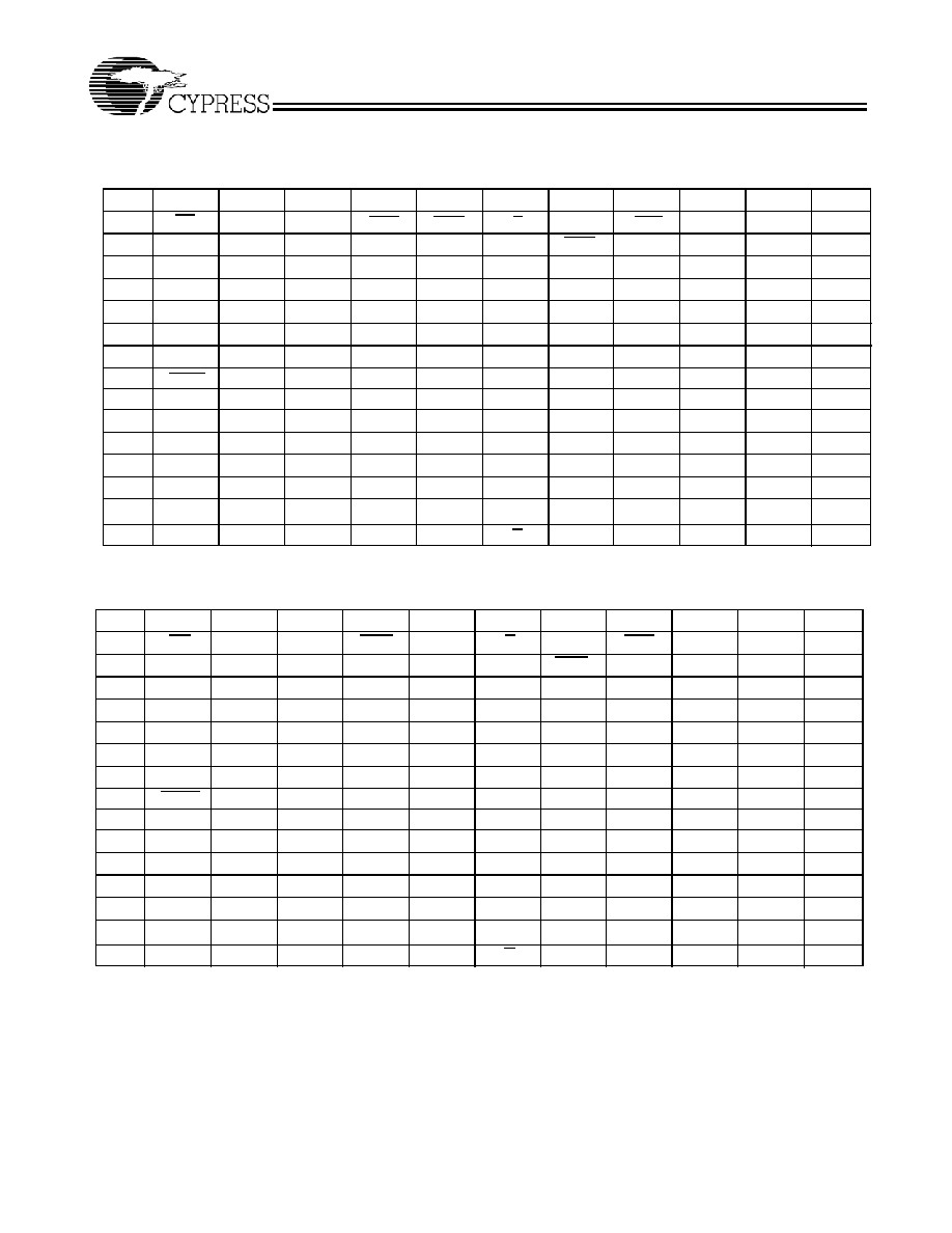
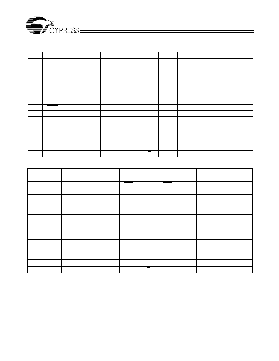
Truth Table
[2, 3, 4, 5, 6, 7]
Operation
K
RPS
WPS
DQ
DQ
Write Cycle:
Load address on the rising edge of K clock;
input write data on K and K rising edges.
L-H
X
L
D(A + 0)at K(t)
D(A + 1) at K(t)
Read Cycle:
Load address on the rising edge of K clock;
wait one and a half cycle; read data on C
and C rising edges.
L-H
L
X
Q(A + 0) at C(t + 1)
Q(A + 1) at C(t + 2)
NOP: No Operation
L-H
H
H
D = X
Q = High-Z
D = X
Q = High-Z
Standby: Clock Stopped
Stopped
X
X
Previous State
Previous State
Write Cycle Descriptions
(CY7C1410AV18 and CY7C1412AV18)
[2, 8]
BWS
0
/NWS
0
BWS
1
/ NWS
1
K
K
Comments
L
L
L-H
≠
During the Data portion of a Write sequence
:
CY7C1410AV18
-
both nibbles (D
[7:0]
) are written into the device,
CY7C1412AV18
-
both bytes (D
[17:0]
) are written into the device.
L
L
≠
L-H During the Data portion of a Write sequence
:
CY7C1410AV18
-
both nibbles (D
[7:0]
) are written into the device,
CY7C1412AV18
-
both bytes (D
[17:0]
) are written into the device.
L
H
L-H
≠
During the Data portion of a Write sequence
:
CY7C1410AV18
-
only the lower nibble (D
[3:0]
) is written into the device. D
[7:4]
will
remain unaltered,
CY7C1412AV18
-
only the lower byte (D
[8:0]
) is written into the device. D
[17:9]
will
remain unaltered.
Notes:
1. The above application shows four QDR-II being used.
2. X = "Don't Care," H = Logic HIGH, L= Logic LOW,
represents rising edge.
3. Device will power-up deselected and the outputs in a three-state condition.
4. "A" represents address location latched by the devices when transaction was initiated. A + 00, A + 01 represents the internal address sequence in the burst.
5. "t" represents the cycle at which a Read/Write operation is started. t + 1 and t + 2 are the first and second clock cycles respectively succeeding the "t" clock cycle.
6. Data inputs are registered at K and K rising edges. Data outputs are delivered on C and C rising edges, except when in single clock mode.
7. It is recommended that K = K and C = C = HIGH when clock is stopped. This is not essential, but permits most rapid restart by overcoming transmission line
charging symmetrically.
8. Assumes a Write cycle was initiated per the Write Port Cycle Description Truth Table. NWS
0
, NWS
1
, BWS
0
, BWS
1
, BWS
2
and BWS
3
can be altered on different
portions of a Write cycle, as long as the set-up and hold requirements are achieved.
Vt = Vddq/2
C C#
D
A
K
C C#
D
A
K
BUS
MASTER
(CPU
or
ASIC)
SRAM #1
SRAM #4
DATA IN
DATA OUT
Address
RPS#
WPS#
BWS#
Source K
Source K#
Delayed K
Delayed K#
R = 50
µ
R = 250
µ
R = 250
µ
R
P
S
#
W
P
S
#
B
W
S
#
R
P
S
#
W
P
S
#
B
W
S
#
Vt
Vt
Vt
R
R
R
ZQ
CQ/CQ#
Q
K#
ZQ
CQ/CQ#
Q
K#
CLKIN/CLKIN#
PRELIMINARY
CY7C1410AV18
CY7C1425AV18
CY7C1412AV18
CY7C1414AV18
Document #: 38-05615 Rev. **
Page 10 of 23
L
H
≠
L-H During the Data portion of a Write sequence
:
CY7C1410AV18
-
only the lower nibble (D
[3:0]
) is written into the device. D
[7:4]
will
remain unaltered,
CY7C1412AV18
-
only the lower byte (D
[8:0]
) is written into the device. D
[17:9]
will
remain unaltered.
H
L
L-H
≠
During the Data portion of a Write sequence
:
CY7C1410AV18
-
only the upper nibble (D
[7:4]
) is written into the device. D
[3:0]
will
remain unaltered,
CY7C1412AV18
-
only the upper byte (D
[17:9]
) is written into the device. D
[8:0]
will
remain unaltered.
H
L
≠
L-H During the Data portion of a Write sequence
:
CY7C1410AV18
-
only the upper nibble (D
[7:4]
) is written into the device. D
[3:0]
will
remain unaltered,
CY7C1412AV18
-
only the upper byte (D
[17:9]
) is written into the device. D
[8:0]
will
remain unaltered.
H
H
L-H
≠
No data is written into the devices during this portion of a Write operation.
H
H
≠
L-H No data is written into the devices during this portion of a Write operation.
Write Cycle Descriptions
(CY7C1414AV18)
[2, 8]
BWS
0
BWS
1
BWS
2
BWS
3
K
K
Comments
L
L
L
L
L-H
-
During the Data portion of a Write sequence, all four bytes (D
[35:0]
) are written
into the device.
L
L
L
L
-
L-H During the Data portion of a Write sequence, all four bytes (D
[35:0]
) are written
into the device.
L
H
H
H
L-H
-
During the Data portion of a Write sequence, only the lower byte (D
[8:0]
) is written
into the device. D
[35:9]
will remain unaltered.
L
H
H
H
-
L-H During the Data portion of a Write sequence, only the lower byte (D
[8:0]
) is written
into the device. D
[35:9]
will remain unaltered.
H
L
H
H
L-H
-
During the Data portion of a Write sequence, only the byte (D
[17:9]
) is written into
the device. D
[8:0]
and D
[35:18]
will remain unaltered.
H
L
H
H
-
L-H During the Data portion of a Write sequence, only the byte (D
[17:9]
) is written into
the device. D
[8:0]
and D
[35:18]
will remain unaltered.
H
H
L
H
L-H
-
During the Data portion of a Write sequence, only the byte (D
[26:18]
) is written into
the device. D
[17:0]
and D
[35:27]
will remain unaltered.
H
H
L
H
-
L-H During the Data portion of a Write sequence, only the byte (D
[26:18]
) is written into
the device. D
[17:0]
and D
[35:27]
will remain unaltered.
H
H
H
L
L-H
During the Data portion of a Write sequence, only the byte (D
[35:27]
) is written into
the device. D
[26:0]
will remain unaltered.
H
H
H
L
-
L-H During the Data portion of a Write sequence, only the byte (D
[35:27]
) is written into
the device. D
[26:0]
will remain unaltered.
H
H
H
H
L-H
-
No data is written into the device during this portion of a Write operation.
H
H
H
H
-
L-H No data is written into the device during this portion of a Write operation.
Write Cycle Descriptions
(CY7C1425AV18)
BWS
0
K
K
Comments
L
L-H
≠
During the Data portion of a Write sequence
:
CY7C1425AV18
- the single byte
(D
[8:0]
) is written into the device
L
≠
L-H
During the Data portion of a Write sequence
:
CY7C1425AV18
- the single byte
(D
[8:0]
) is written into the device,
H
L-H
≠
No data is written into the devices during this portion of a Write operation.
H
≠
L-H
No data is written into the devices during this portion of a Write operation.
Write Cycle Descriptions
(CY7C1410AV18 and CY7C1412AV18) (continued)
[2, 8]
BWS
0
/NWS
0
BWS
1
/ NWS
1
K
K
Comments
PRELIMINARY
CY7C1410AV18
CY7C1425AV18
CY7C1412AV18
CY7C1414AV18
Document #: 38-05615 Rev. **
Page 11 of 23
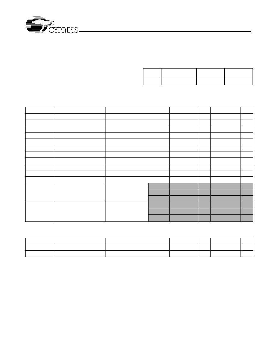
Maximum Ratings
(Above which the useful life may be impaired.)
Storage Temperature .................................≠65∞C to +150∞C
Ambient Temperature with
Power Applied...............................................≠10∞C to +85∞C
Supply Voltage on V
DD
Relative to GND........ ≠0.5V to +2.9V
DC Voltage Applied to Outputs
in High-Z State .................................... ≠0.5V to V
DDQ
+ 0.3V
DC Input Voltage
[12]
............................ ≠0.5V to V
DDQ
+ 0.3V
Current into Outputs (LOW)......................................... 20 mA
Static Discharge Voltage.......................................... > 2001V
(per MIL-STD-883, Method 3015)
Latch-up Current.................................................... > 200 mA
Operating Range
Range
Ambient
Temperature (T
A
)
V
DD
[13]
V
DDQ
[13]
Com'l
0∞C to +70∞C
1.8
±
0.1 V
1.4V to V
DD
Electrical Characteristics
Over the Operating Range
[9, 13]
DC Electrical Characteristics Over the Operating Range
Parameter
Description
Test Conditions
Min.
Typ.
Max.
Unit
V
DD
Power Supply Voltage
1.7
1.8
1.9
V
V
DDQ
I/O Supply Voltage
1.4
1.5
V
DD
V
V
OH
Output HIGH Voltage
[10]
V
DDQ
/2 ≠ 0.12
V
DDQ
/2 + 0.12
V
V
OL
Output LOW Voltage
[11]
V
DDQ
/2 ≠ 0.12
V
DDQ
/2 + 0.12
V
V
OH(LOW)
Output HIGH Voltage
I
OH
=
-
0.1 mA, Nominal Impedance
V
DDQ
≠ 0.2
V
DDQ
V
V
OL(LOW)
Output LOW Voltage
I
OL
= 0.1 mA, Nominal Impedance
V
SS
0.2
V
V
IH
Input HIGH Voltage
[12]
V
REF
+ 0.1
V
DDQ
+0.3
V
V
IL
Input LOW Voltage
[12]
≠0.3
V
REF
≠ 0.1
V
I
X
Input Load Current
GND
V
I
V
DDQ
-
5
5
µ
A
I
OZ
Output Leakage Current
GND
V
I
V
DDQ,
Output Disabled
-
5
5
µ
A
V
REF
Input Reference Voltage
[14]
Typical Value = 0.75V
0.68
0.75
0.95
V
I
DD
V
DD
Operating Supply
V
DD
= Max., I
OUT
= 0
mA, f = f
MAX
= 1/t
CYC
167 MHz
TBD
mA
200 MHz
TBD
mA
250 MHz
TBD
mA
I
SB1
Automatic Power-down
Current
Max. V
DD
, Both Ports
Deselected, V
IN
V
IH
or V
IN
V
IL
f = f
MAX
=
1/t
CYC,
Inputs Static
167 MHz
TBD
mA
200 MHz
TBD
mA
250 MHz
TBD
mA
Shaded areas contain advance information.
Please contact your local Cypress Sales representative for availability of these parts.
AC Input Requirements Over the Operating Range
Parameter
Description
Test Conditions
Min.
Typ.
Max.
Unit
V
IH
Input High (Logic 1) Voltage
V
REF
+ 0.2
≠
≠
V
V
IL
Input Low (Logic 0) Voltage
≠
≠
V
REF
- 0.2
V
Notes:
9. All voltage referenced to Ground.
10. Output are impedance controlled. I
OH
= ≠(V
DDQ
/2)/(RQ/5) for values of 175
<= RQ <= 350
s.
11. Output are impedance controlled. I
OL
= (V
DDQ
/2)/(RQ/5) for values of 175
<= RQ <= 350
.
12. Overshoot: V
IH
(AC) < V
DDQ
+0.85V (Pulse width less than t
CYC
/2), Undershoot: V
IL
(AC) > ≠1.5V (Pulse width less than t
CYC
/2).
13. Power-up: Assumes a linear ramp from 0V to V
DD
(min.) within 200 ms. During this time V
IH
< V
DD
and V
DDQ
< V
DD
.
14. V
REF
(Min.) = 0.68V or 0.46V
DDQ
, whichever is larger, V
REF
(Max.) = 0.95V or 0.54V
DDQ
, whichever is smaller.
PRELIMINARY
CY7C1410AV18
CY7C1425AV18
CY7C1412AV18
CY7C1414AV18
Document #: 38-05615 Rev. **
Page 12 of 23
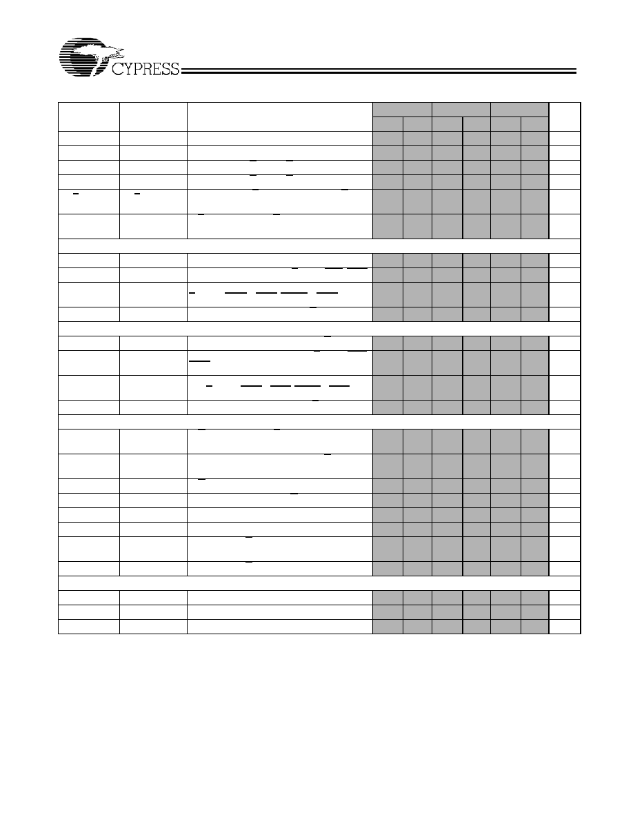
Switching Characteristics
Over the Operating Range
[15,16]
Cypress
Parameter
Consortium
Parameter
Description
250 MHz
200 MHz
167 MHz
Unit
Min. Max. Min. Max. Min. Max.
t
POWER
V
DD
(Typical) to the first Access
[19]
1
1
1
ms
t
CYC
t
KHKH
K Clock and C Clock Cycle Time
4.0
6.3
5.0
7.9
6.0
8.4
ns
t
KH
t
KHKL
Input Clock (K/K and C/C) HIGH
1.6
≠
2.0
≠
2.4
≠
ns
t
KL
t
KLKH
Input Clock (K/K and C/C) LOW
1.6
≠
2.0
≠
2.4
≠
ns
t
KHKH
t
KHKH
K Clock Rise to K Clock Rise and C to C Rise
(rising edge to rising edge)
1.8
≠
2.2
≠
2.7
≠
ns
t
KHCH
t
KHCH
K/K Clock Rise to C/C Clock Rise (rising
edge to rising edge)
0.0
1.8
0.0
2.2
0.0
2.7
ns
Set-up Times
t
SA
t
SA
Address Set-up to K Clock Rise
0.35
≠
0.4
≠
0.5
≠
ns
t
SC
t
SC
Control Set-up to Clock (K, K) Rise (RPS, WPS)
0.5
≠
0.6
≠
0.7
≠
ns
t
SCDDR
t
SC
Double Data Rate Control Set-up to Clock (K,
K) Rise (BWS
0
, BWS
1
, BWS
3
, BWS
4
)
0.35
≠
0.4
≠
0.5
≠
ns
t
SD
t
SD
D
[X:0]
Set-up to Clock (K and K) Rise
0.35
≠
0.4
≠
0.5
≠
ns
Hold Times
t
HA
t
HA
Address Hold after Clock (K and K) Rise
0.35
≠
0.4
≠
0.5
≠
ns
t
HC
t
HC
Control Hold after Clock (K and K) Rise (RPS,
WPS)
0.5
≠
0.6
≠
0.7
≠
ns
t
HCDDR
t
HC
Double Data Rate Control Hold after Clock (K
and K) Rise (BWS
0
, BWS
1
, BWS
3
, BWS
4
)
0.35
≠
0.4
≠
0.5
≠
ns
t
HD
t
HD
D
[X:0]
Hold after Clock (K and K) Rise
0.35
≠
0.4
≠
0.5
≠
ns
Output Times
t
CO
t
CHQV
C/C Clock Rise (or K/K in Single Clock Mode)
to Data Valid
≠
0.45
≠
0.45
≠
0.50
ns
t
DOH
t
CHQX
Data Output Hold after Output C/C Clock
Rise (Active to Active)
≠0.45
≠
-0.45
≠
-0.50
≠
ns
t
CCQO
t
CHCQV
C/C Clock Rise to Echo Clock Valid
≠
0.45
≠
0.45
≠
0.50
ns
t
CQOH
t
CHCQX
Echo Clock Hold after C/C Clock Rise
≠0.45
≠
≠0.45
≠
≠0.50
≠
ns
t
CQD
t
CQHQV
Echo Clock High to Data Valid
≠
0.30
≠
0.35
≠
0.40
ns
t
CQDOH
t
CQHQX
Echo Clock High to Data Invalid
≠0.30
≠
≠0.35
≠
≠0.40
≠
ns
t
CHZ
t
CHZ
Clock (C and C) Rise to High-Z (Active to
High-Z)
[17,18]
≠
0.45
≠
0.45
≠
0.50
ns
t
CLZ
t
CLZ
Clock (C and C) Rise to Low-Z
[17,18]
≠0.45
≠
≠0.45
≠
≠0.50
≠
ns
DLL Timing
t
KC Var
t
KC Var
Clock Phase Jitter
≠
0.20
≠
0.20
≠
0.20
ns
t
KC lock
t
KC lock
DLL Lock Time (K, C)
1024
≠
1024
≠
1024
≠
cycles
t
KC Reset
t
KC Reset
K Static to DLL Reset
30
≠
30
≠
30
≠
ns
Shaded areas contain advance information.
Please contact your local Cypress Sales representative for availability of these parts.
Notes:
15. All devices can operate at clock frequencies as low as 119 MHz. When a part with a maximum frequency above 133 MHz is operating at a lower clock frequency,
it requires the input timings of the frequency range in which it is being operated and will output data with the output timings of that frequency range.
16. Unless otherwise noted, test conditions assume signal transition time of 2V/ns, timing reference levels of 0.75V, Vref = 0.75V, RQ = 250
, V
DDQ
= 1.5V, input
pulse levels of 0.25V to 1.25V, and output loading of the specified I
OL
/I
OH
and load capacitance shown in (a) of AC Test Loads.
17. t
CHZ
, t
CLZ
, are specified with a load capacitance of 5 pF as in part (b) of AC Test Loads. Transition is measured
±
100 mV from steady-state voltage.
18. At any given voltage and temperature t
CHZ
is less than t
CLZ
and t
CHZ
less than t
CO
.
19. This part has a voltage regulator internally; t
POWER
is the time that the power needs to be supplied above V
DD
minimum initially before a read or write operation
can be initiated.
PRELIMINARY
CY7C1410AV18
CY7C1425AV18
CY7C1412AV18
CY7C1414AV18
Document #: 38-05615 Rev. **
Page 13 of 23
Note:
20. Tested initially and after any design or process change that may affect these parameters.
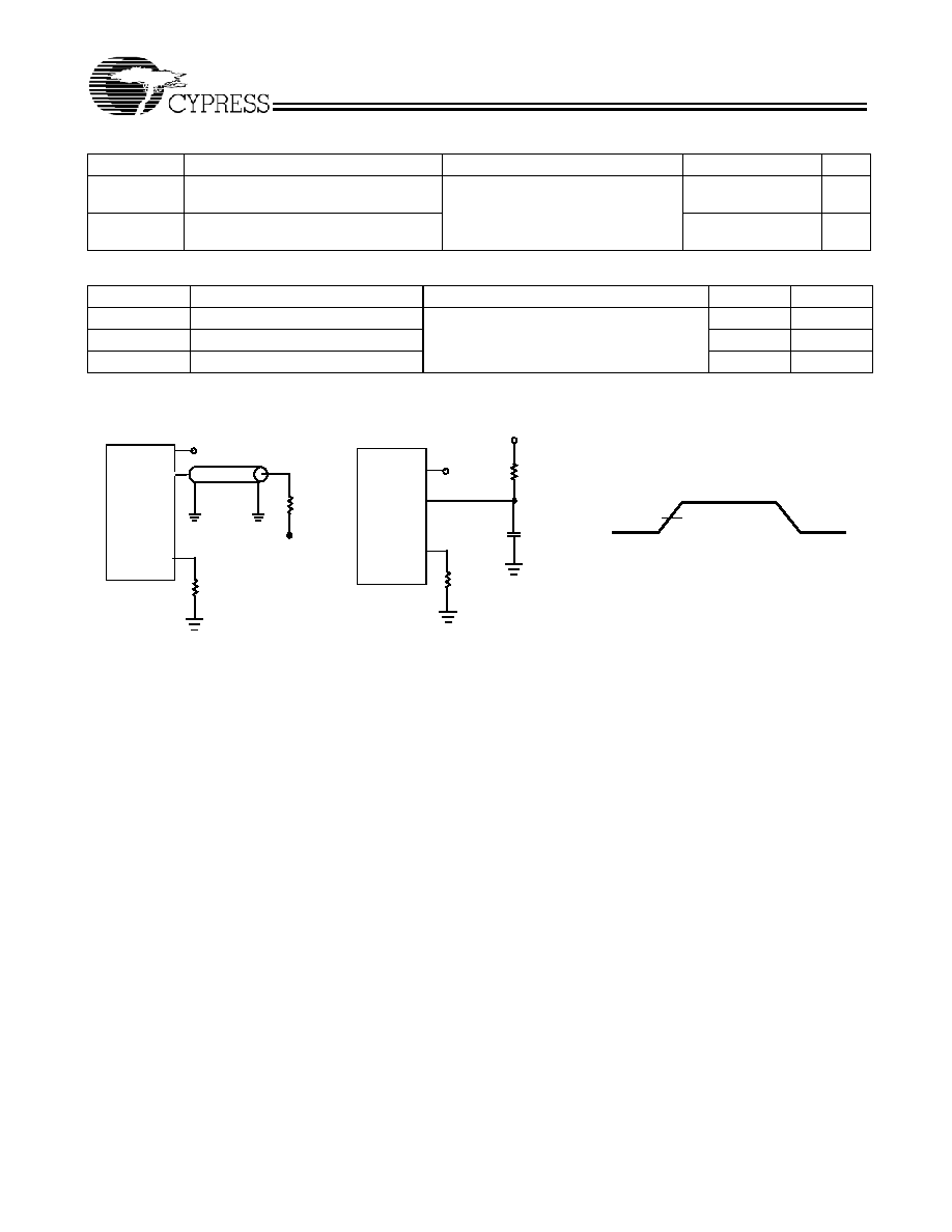
Thermal Resistance
[20]
Parameter
Description
Test Conditions
165 FBGA Package
Unit
JA
Thermal Resistance
(Junction to Ambient)
Test conditions follow standard test
methods and procedures for
measuring thermal impedance, per
EIA/JESD51.
TBD
∞
C/W
JC
Thermal Resistance
(Junction to Case)
TBD
∞
C/W
Capacitance
[20]
Parameter
Description
Test Conditions
Max.
Unit
C
IN
Input
Capacitance
T
A
= 25
∞
C, f = 1 MHz,
V
DD
= 1.8V
V
DDQ
= 1.5V
TBD
pF
C
CLK
Clock Input Capacitance
TBD
pF
C
O
Output Capacitance
TBD
pF
AC Test Loads and Waveforms
1.25V
0.25V
R = 50
5 pF
INCLUDING
JIG AND
SCOPE
ALL INPUT PULSES
Device
R
L
= 50
Z
0
= 50
V
REF
= 0.75V
V
REF
= 0.75V
[12]
0.75V
Under
Test
0.75V
Device
Under
Test
OUTPUT
0.75V
V
REF
V
REF
OUTPUT
ZQ
ZQ
(a)
RQ =
250
(b)
RQ =
250
Slew Rate = 2V / ns
PRELIMINARY
CY7C1410AV18
CY7C1425AV18
CY7C1412AV18
CY7C1414AV18
Document #: 38-05615 Rev. **
Page 14 of 23
Switching Waveforms
[21, 22, 23]
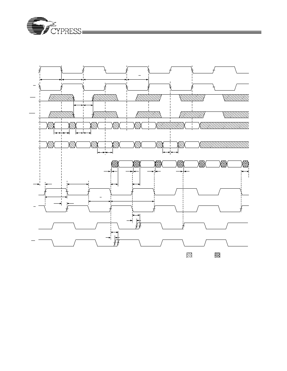
Read/Write/Deselect Sequence
Notes:
21. Q00 refers to output from address A0. Q01 refers to output from the next internal burst address following A0, i.e., A0 + 1.
22. Output are disabled (High-Z) one clock cycle after a NOP.
23. In this example, if address A2 = A1,then data Q20 = D10 and Q21 = D11. Write data is forwarded immediately as read results. This note applies to the whole
diagram.
K
1
2
3
4
5
8
10
6
7
K
RPS
WPS
A
Q
D
C
C
A0
READ
READ
WRITE
WRITE
WRITE
tKH
tKHKH
tKHCH
tCO
tKL
tCYC
t
tHC
tSA tHA
tSD
tHD
tKHCH
NOP
DON'T CARE
UNDEFINED
tCLZ
tCHZ
SC
tKH
tKL
t
tSA tHA
D30
D50
D51
D61
tSD
tHD
READ
WRITE
NOP
Q00
Q01
Q20
tCO
tDOH
tKHKH
t CYC
9
A6
A5
A3
A4
A1
A2
Q21
Q40
Q41
D31
D11
D10
D60
tCQD
tDOH
CQ
CQ
tCCQO
tCQOH
tCCQO
tCQOH

PRELIMINARY
CY7C1410AV18
CY7C1425AV18
CY7C1412AV18
CY7C1414AV18
Document #: 38-05615 Rev. **
Page 15 of 23
IEEE 1149.1 Serial Boundary Scan (JTAG)
These SRAMs incorporate a serial boundary scan test access
port (TAP) in the FBGA package. This part is fully compliant
with IEEE Standard #1149.1-1900. The TAP operates using
JEDEC standard 1.8V I/O logic levels.
Disabling the JTAG Feature
It is possible to operate the SRAM without using the JTAG
feature. To disable the TAP controller, TCK must be tied LOW
(V
SS
) to prevent clocking of the device. TDI and TMS are inter-
nally pulled up and may be unconnected. They may alternately
be connected to V
DD
through a pull-up resistor. TDO should
be left unconnected. Upon power-up, the device will come up
in a reset state which will not interfere with the operation of the
device.
Test Access Port--Test Clock
The test clock is used only with the TAP controller. All inputs
are captured on the rising edge of TCK. All outputs are driven
from the falling edge of TCK.
Test Mode Select
The TMS input is used to give commands to the TAP controller
and is sampled on the rising edge of TCK. It is allowable to
leave this pin unconnected if the TAP is not used. The pin is
pulled up internally, resulting in a logic HIGH level.
Test Data-In (TDI)
The TDI pin is used to serially input information into the
registers and can be connected to the input of any of the
registers. The register between TDI and TDO is chosen by the
instruction that is loaded into the TAP instruction register. For
information on loading the instruction register, see the TAP
Controller State Diagram. TDI is internally pulled up and can
be unconnected if the TAP is unused in an application. TDI is
connected to the most significant bit (MSB) on any register.
Test Data-Out (TDO)
The TDO output pin is used to serially clock data-out from the
registers. The output is active depending upon the current
state of the TAP state machine (see Instruction codes). The
output changes on the falling edge of TCK. TDO is connected
to the least significant bit (LSB) of any register.
Performing a TAP Reset
A Reset is performed by forcing TMS HIGH (VDD) for five
rising edges of TCK. This RESET does not affect the operation
of the SRAM and may be performed while the SRAM is
operating. At power-up, the TAP is reset internally to ensure
that TDO comes up in a high-Z state.
TAP Registers
Registers are connected between the TDI and TDO pins and
allow data to be scanned into and out of the SRAM test
circuitry. Only one register can be selected at a time through
the instruction registers. Data is serially loaded into the TDI pin
on the rising edge of TCK. Data is output on the TDO pin on
the falling edge of TCK.
Instruction Register
Three-bit instructions can be serially loaded into the instruction
register. This register is loaded when it is placed between the
TDI and TDO pins as shown in TAP Controller Block Diagram.
Upon power-up, the instruction register is loaded with the
IDCODE instruction. It is also loaded with the IDCODE
instruction if the controller is placed in a reset state as
described in the previous section.
When the TAP controller is in the Capture IR state, the two
least significant bits are loaded with a binary "01" pattern to
allow for fault isolation of the board level serial test path.
Bypass Register
To save time when serially shifting data through registers, it is
sometimes advantageous to skip certain chips. The bypass
register is a single-bit register that can be placed between TDI
and TDO pins. This allows data to be shifted through the
SRAM with minimal delay. The bypass register is set LOW
(V
SS
) when the BYPASS instruction is executed.
Boundary Scan Register
The boundary scan register is connected to all of the input and
output pins on the SRAM. Several no connect (NC) pins are
also included in the scan register to reserve pins for higher
density devices.
The boundary scan register is loaded with the contents of the
RAM Input and Output ring when the TAP controller is in the
Capture-DR state and is then placed between the TDI and
TDO pins when the controller is moved to the Shift-DR state.
The EXTEST, SAMPLE/PRELOAD and SAMPLE Z instruc-
tions can be used to capture the contents of the Input and
Output ring.
The Boundary Scan Order tables show the order in which the
bits are connected. Each bit corresponds to one of the bumps
on the SRAM package. The MSB of the register is connected
to TDI, and the LSB is connected to TDO.
Identification (ID) Register
The ID register is loaded with a vendor-specific, 32-bit code
during the Capture-DR state when the IDCODE command is
loaded in the instruction register. The IDCODE is hardwired
into the SRAM and can be shifted out when the TAP controller
is in the Shift-DR state. The ID register has a vendor code and
other information described in the Identification Register
Definitions table.
TAP Instruction Set
Eight different instructions are possible with the three-bit
instruction register. All combinations are listed in the
Instruction Code table. Three of these instructions are listed
as RESERVED and should not be used. The other five instruc-
tions are described in detail below.
Instructions are loaded into the TAP controller during the
Shift-IR state when the instruction register is placed between
TDI and TDO. During this state, instructions are shifted
through the instruction register through the TDI and TDO pins.
To execute the instruction once it is shifted in, the TAP
controller needs to be moved into the Update-IR state.
IDCODE
The IDCODE instruction causes a vendor-specific, 32-bit code
to be loaded into the instruction register. It also places the
instruction register between the TDI and TDO pins and allows
the IDCODE to be shifted out of the device when the TAP
controller enters the Shift-DR state. The IDCODE instruction

PRELIMINARY
CY7C1410AV18
CY7C1425AV18
CY7C1412AV18
CY7C1414AV18
Document #: 38-05615 Rev. **
Page 16 of 23
is loaded into the instruction register upon power-up or
whenever the TAP controller is given a test logic reset state.
SAMPLE Z
The SAMPLE Z instruction causes the boundary scan register
to be connected between the TDI and TDO pins when the TAP
controller is in a Shift-DR state. The SAMPLE Z command puts
the output bus into a High-Z state until the next command is
given during the "Update IR" state.
SAMPLE/PRELOAD
SAMPLE/PRELOAD is a 1149.1 mandatory instruction. When
the SAMPLE/PRELOAD instructions are loaded into the
instruction register and the TAP controller is in the Capture-DR
state, a snapshot of data on the inputs and output pins is
captured in the boundary scan register.
The user must be aware that the TAP controller clock can only
operate at a frequency up to 20 MHz, while the SRAM clock
operates more than an order of magnitude faster. Because
there is a large difference in the clock frequencies, it is
possible that during the Capture-DR state, an input or output
will undergo a transition. The TAP may then try to capture a
signal while in transition (metastable state). This will not harm
the device, but there is no guarantee as to the value that will
be captured. Repeatable results may not be possible.
To guarantee that the boundary scan register will capture the
correct value of a signal, the SRAM signal must be stabilized
long enough to meet the TAP controller's capture set-up plus
hold times (t
CS
and t
CH
). The SRAM clock input might not be
captured correctly if there is no way in a design to stop (or
slow) the clock during a SAMPLE/PRELOAD instruction. If this
is an issue, it is still possible to capture all other signals and
simply ignore the value of the CK and CK captured in the
boundary scan register.
Once the data is captured, it is possible to shift out the data by
putting the TAP into the Shift-DR state. This places the
boundary scan register between the TDI and TDO pins.
PRELOAD allows an initial data pattern to be placed at the
latched parallel outputs of the boundary scan register cells
prior to the selection of another boundary scan test operation.
The shifting of data for the SAMPLE and PRELOAD phases
can occur concurrently when required--that is, while data
captured is shifted out, the preloaded data can be shifted in.
BYPASS
When the BYPASS instruction is loaded in the instruction
register and the TAP is placed in a Shift-DR state, the bypass
register is placed between the TDI and TDO pins. The
advantage of the BYPASS instruction is that it shortens the
boundary scan path when multiple devices are connected
together on a board.
EXTEST
The EXTEST instruction enables the preloaded data to be
driven out through the system output pins. This instruction also
selects the boundary scan register to be connected for serial
access between the TDI and TDO in the shift-DR controller
state.
EXTEST OUTPUT BUS THREE-STATE
IEEE Standard 1149.1 mandates that the TAP controller be
able to put the output bus into a three-state mode.
The boundary scan register has a special bit located at bit #47.
When this scan cell, called the "extest output bus three-state,"
is latched into the preload register during the "Update-DR"
state in the TAP controller, it will directly control the state of the
output (Q-bus) pins, when the EXTEST is entered as the
current instruction. When HIGH, it will enable the output
buffers to drive the output bus. When LOW, this bit will place
the output bus into a High-Z condition.
This bit can be set by entering the SAMPLE/PRELOAD or
EXTEST command, and then shifting the desired bit into that
cell, during the "Shift-DR" state. During "Update-DR", the value
loaded into that shift-register cell will latch into the preload
register. When the EXTEST instruction is entered, this bit will
directly control the output Q-bus pins. Note that this bit is
pre-set LOW to enable the output when the device is
powered-up, and also when the TAP controller is in the
"Test-Logic-Reset" state.
Reserved
These instructions are not implemented but are reserved for
future use. Do not use these instructions.
PRELIMINARY
CY7C1410AV18
CY7C1425AV18
CY7C1412AV18
CY7C1414AV18
Document #: 38-05615 Rev. **
Page 17 of 23
Note:
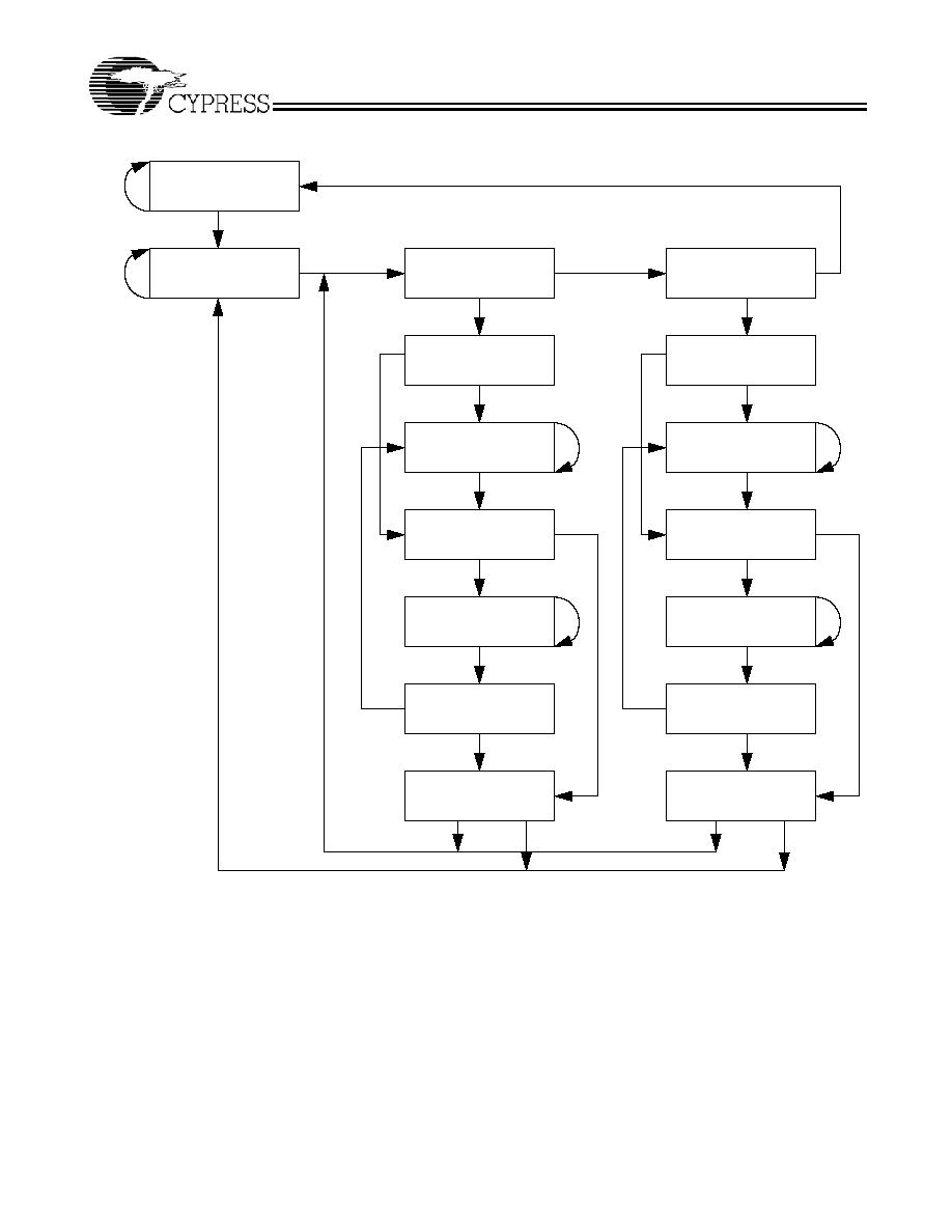
24. The 0/1 next to each state represents the value at TMS at the rising edge of TCK.
TAP Controller State Diagram
[24]
TEST-LOGIC
RESET
TEST-LOGIC/
IDLE
SELECT
DR-SCAN
CAPTURE-DR
SHIFT-DR
EXIT1-DR
PAUSE-DR
EXIT2-DR
UPDATE-DR
SELECT
IR-SCAN
CAPTURE-IR
SHIFT-IR
EXIT1-IR
PAUSE-IR
EXIT2-IR
UPDATE-IR
1
0
1
1
0
1
0
1
0
0
0
1
1
1
0
1
0
1
0
0
0
1
0
1
1
0
1
0
0
1
1
0
PRELIMINARY
CY7C1410AV18
CY7C1425AV18
CY7C1412AV18
CY7C1414AV18
Document #: 38-05615 Rev. **
Page 18 of 23
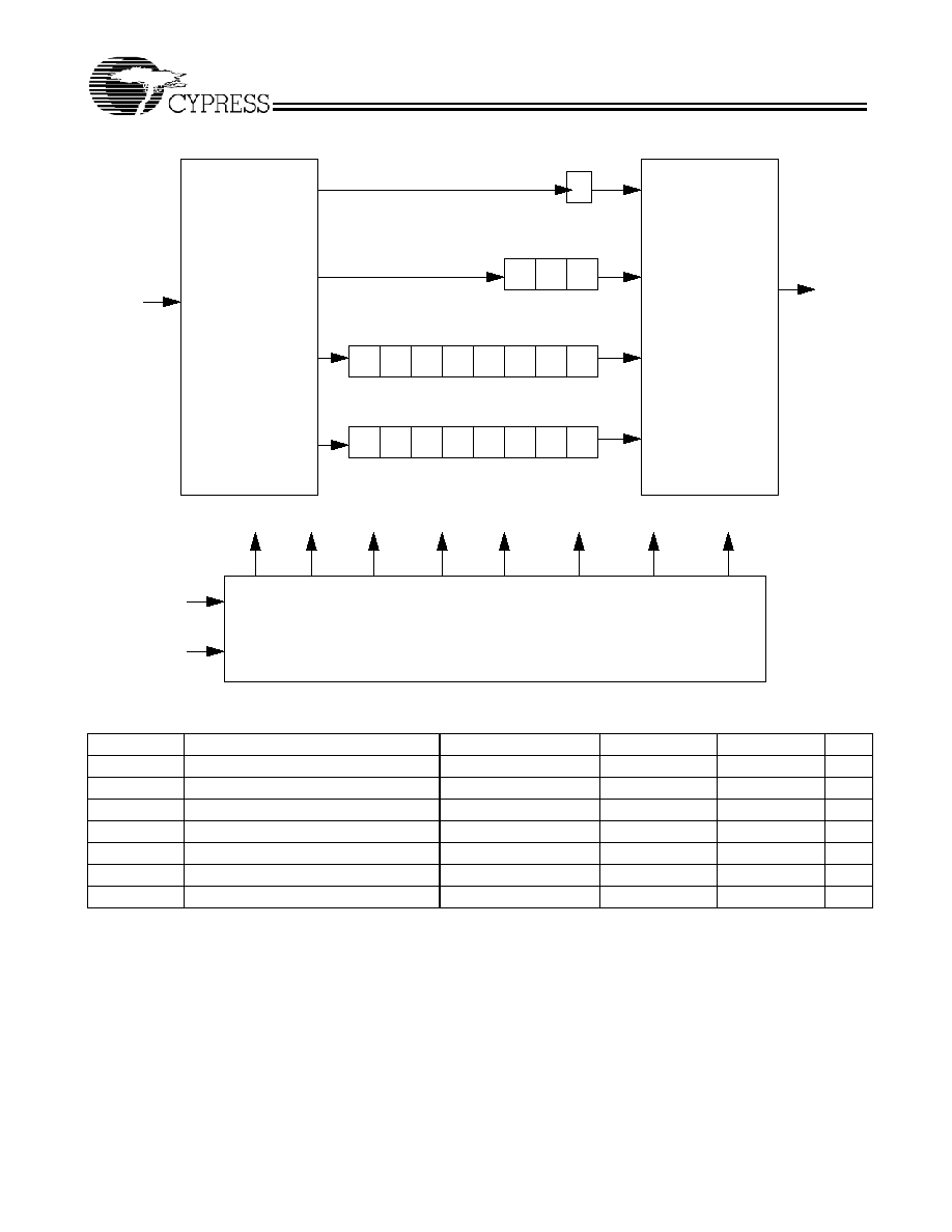
TAP Controller Block Diagram
0
0
1
2
.
.
29
30
31
Boundary Scan Register
Identification Register
0
1
2
.
.
.
.
106
0
1
2
Instruction Register
Bypass Register
Selection
Circuitry
Selection
Circuitry
TAP Controller
TDI
TDO
TCK
TMS
TAP Electrical Characteristics
Over the Operating Range
[9, 12, 25]
Parameter
Description
Test Conditions
Min.
Max.
Unit
V
OH1
Output HIGH Voltage
I
OH
=
-
2.0 mA
1.4
V
V
OH2
Output HIGH Voltage
I
OH
=
-
100
µ
A
1.6
V
V
OL1
Output LOW Voltage
I
OL
= 2.0 mA
0.4
V
V
OL2
Output LOW Voltage
I
OL
= 100
µ
A
0.2
V
V
IH
Input HIGH Voltage
0.65V
DD
V
DD
+ 0.3
V
V
IL
Input LOW Voltage
≠0.3
0.35V
DD
V
I
X
Input and OutputLoad Current
GND
V
I
V
DD
-
5
5
µ
A
Notes:
25. These characteristic pertain to the TAP inputs (TMS, TCK, TDI and TDO). Parallel load levels are specified in the Electrical Characteristics table.
PRELIMINARY
CY7C1410AV18
CY7C1425AV18
CY7C1412AV18
CY7C1414AV18
Document #: 38-05615 Rev. **
Page 19 of 23
TAP AC Switching Characteristics
Over the Operating Range
[26, 27]
Parameter
Description
Min.
Max.
Unit
t
TCYC
TCK Clock Cycle Time
50
ns
t
TF
TCK Clock Frequency
20
MHz
t
TH
TCK Clock HIGH
40
ns
t
TL
TCK Clock LOW
40
ns
Set-up Times
t
TMSS
TMS Set-up to TCK Clock Rise
10
ns
t
TDIS
TDI Set-up to TCK Clock Rise
10
ns
t
CS
Capture Set-up to TCK Rise
10
ns
Hold Times
t
TMSH
TMS Hold after TCK Clock Rise
10
ns
t
TDIH
TDI Hold after Clock Rise
10
ns
t
CH
Capture Hold after Clock Rise
10
ns
Output Times
t
TDOV
TCK Clock LOW to TDO Valid
20
ns
t
TDOX
TCK Clock LOW to TDO Invalid
0
ns
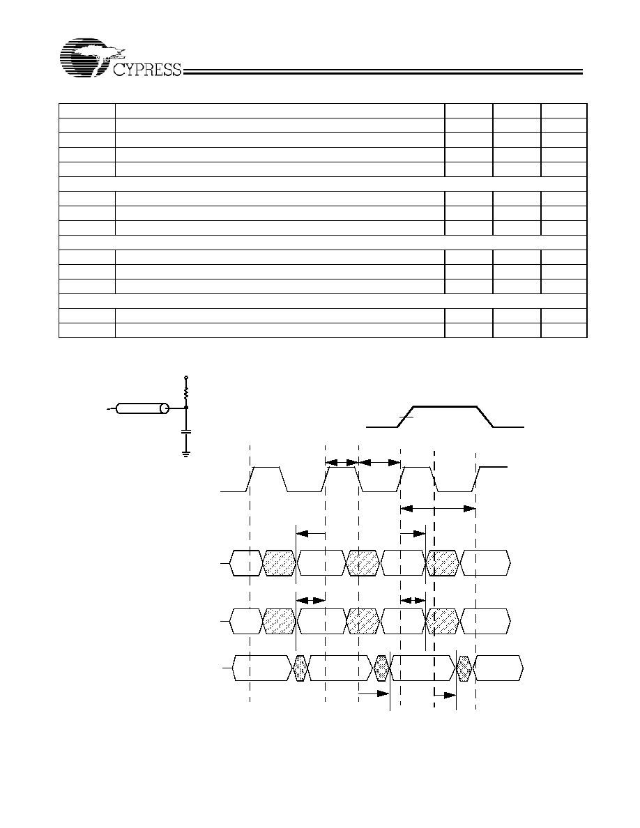
TAP Timing and Test Conditions
[27]
Notes:
26. t
CS
and t
CH
refer to the set-up and hold time requirements of latching data from the boundary scan register.
27. Test conditions are specified using the load in TAP AC test conditions. t
R
/t
F
= 1 ns.
(a)
TDO
C
L
= 20 pF
Z
0
= 50
GND
0.9V
50
1.8V
0V
ALL INPUT PULSES
0.9V
Test Clock
Test Mode Select
TCK
TMS
Test Data-In
TDI
Test Data-Out
t
TCYC
t
TMSH
t
TL
t
TH
t
TMSS
t
TDIS
t
TDIH
t
TDOV
t
TDOX
TDO
PRELIMINARY
CY7C1410AV18
CY7C1425AV18
CY7C1412AV18
CY7C1414AV18
Document #: 38-05615 Rev. **
Page 20 of 23
Identification Register Definitions
Instruction Field
Value
Description
CY7C1410AV18
CY7C1425AV18
CY7C1412AV18
CY7C1414AV18
Revision Number
(31:29)
000
000
000
000
Version number.
Cypress Device ID
(28:12)
11010011010000111 11010011010001111 11010011010010111 11010011010100111 Defines the type of
SRAM.
Cypress JEDEC ID
(11:1)
00000110100
00000110100
00000110100
00000110100
Unique identifi-
cation of SRAM
vendor.
ID Register Presence
(0)
1
1
1
1
Indicates the
presence of an ID
register.
Scan Register Sizes
Register Name
Bit Size
Instruction
3
Bypass
1
ID
32
Boundary Scan Cells
109
Instruction Codes
Instruction
Code
Description
EXTEST
000
Captures the Input/Output ring contents.
IDCODE
001
Loads the ID register with the vendor ID code and places the register between
TDI and TDO. This operation does not affect SRAM operation.
SAMPLE Z
010
Captures the Input/Output contents. Places the boundary scan register
between TDI and TDO. Forces all SRAM output drivers to a High-Z state.
RESERVED
011
Do Not Use: This instruction is reserved for future use.
SAMPLE/PRELOAD
100
Captures the Input/Output ring contents. Places the boundary scan register
between TDI and TDO. Does not affect the SRAM operation.
RESERVED
101
Do Not Use: This instruction is reserved for future use.
RESERVED
110
Do Not Use: This instruction is reserved for future use.
BYPASS
111
Places the bypass register between TDI and TDO. This operation does not
affect SRAM operation.
Boundary Scan Order
Bit #
Bump ID
0
6R
1
6P
2
6N
3
7P
4
7N
5
7R
6
8R
7
8P
8
9R
9
11P
10
10P
11
10N
12
9P
13
10M
14
11N
15
9M
16
9N
17
11L
18
11M
19
9L
20
10L
21
11K
22
10K
23
9J
Boundary Scan Order
(continued)
Bit #
Bump ID
PRELIMINARY
CY7C1410AV18
CY7C1425AV18
CY7C1412AV18
CY7C1414AV18
Document #: 38-05615 Rev. **
Page 21 of 23
24
9K
25
10J
26
11J
27
11H
28
10G
29
9G
30
11F
31
11G
32
9F
33
10F
34
11E
35
10E
36
10D
37
9E
38
10C
39
11D
40
9C
41
9D
42
11B
43
11C
44
9B
45
10B
46
11A
47
10A
48
9A
49
8B
50
7C
51
6C
52
8A
53
7A
54
7B
55
6B
56
6A
57
5B
58
5A
59
4A
60
5C
61
4B
62
3A
63
2A
64
1A
65
2B
66
3B
67
1C
Boundary Scan Order
(continued)
Bit #
Bump ID
68
1B
69
3D
70
3C
71
1D
72
2C
73
3E
74
2D
75
2E
76
1E
77
2F
78
3F
79
1G
80
1F
81
3G
82
2G
83
1H
84
1J
85
2J
86
3K
87
3J
88
2K
89
1K
90
2L
91
3L
92
1M
93
1L
94
3N
95
3M
96
1N
97
2M
98
3P
99
2N
100
2P
101
1P
102
3R
103
4R
104
4P
105
5P
106
5N
107
5R
108
Internal
Boundary Scan Order
(continued)
Bit #
Bump ID
PRELIMINARY
CY7C1410AV18
CY7C1425AV18
CY7C1412AV18
CY7C1414AV18
Document #: 38-05615 Rev. **
Page 22 of 23
© Cypress Semiconductor Corporation, 2004. The information contained herein is subject to change without notice. Cypress Semiconductor Corporation assumes no responsibility for the use
of any circuitry other than circuitry embodied in a Cypress Semiconductor product. Nor does it convey or imply any license under patent or other rights. Cypress Semiconductor does not authorize
its products for use as critical components in life-support systems where a malfunction or failure may reasonably be expected to result in significant injury to the user. The inclusion of Cypress
Semiconductor products in life-support systems application implies that the manufacturer assumes all risk of such use and in doing so indemnifies Cypress Semiconductor against all charges.
Cypress products are not warranted nor intended to be used for medical, life-support, life-saving, critical control or safety applications, unless pursuant to an express written agreement with Cypress.
QDR RAMs and Quad Data Rate RAMs comprise a new family of products developed by Cypress, Hitachi, IDT, NEC, and Samsung
technology. All product and company names mentioned in this document are the trademarks of their respective holders.
Ordering Information
Speed
(MHz)
Ordering Code
Package
Name
Package Type
Operating
Range
250
CY7C1410AV18-250BZC
BB165E
15 x 17 x 1.4 mm FBGA
Commercial
CY7C1425AV18-250BZC
CY7C1412AV18-250BZC
CY7C1414AV18-250BZC
200
CY7C1410AV18-200BZC
BB165E
15 x 17x 1.4 mm FBGA
Commercial
CY7C1425AV18-200BZC
CY7C1412AV18-200BZC
CY7C1414AV18-200BZC
167
CY7C1410AV18-167BZC
BB165E
15 x 17 x 1.4 mm FBGA
Commercial
CY7C1425AV18-167BZC
CY7C1412AV18-167BZC
CY7C1414AV18-167BZC
Shaded areas contain advance information. Please contact your local Cypress Sales representative for availability of these parts.
Package Diagram
A
1
PIN 1 CORNER
17.00±0.10
15.00±0.10
7.00
1.00
ÿ0.50
(165X)
ÿ0.25 M C A B
ÿ0.05 M C
B
A
0.15(4X)
0.41±0.05
1.40
MAX.
SEATING PLANE
0.53±0.05
0.25
C
0.15
C
PIN 1 CORNER
TOP VIEW
BOTTOM VIEW
2
3
4
5
6
7
8
9
10
10.00
14.00
B
C
D
E
F
G
H
J
K
L
M
N
11
11
10
9
8
6
7
5
4
3
2
1
P
R
P
R
K
M
N
L
J
H
G
F
E
D
C
B
A
C
1.00
5.00
0.36
+0.14
-0.06
165-Ball FBGA (15 x 17 x 1.40 mm) Pkg. Outline (0.50 Ball Dia.) BB165E
51-85195-**

PRELIMINARY
CY7C1410AV18
CY7C1425AV18
CY7C1412AV18
CY7C1414AV18
Document #: 38-05615 Rev. **
Page 23 of 23
Document History Page
Document Title: CY7C1410AV18/CY7C1425AV18/CY7C1412AV18/CY7C1414AV18 36-Mbit QDR-IITM SRAM 2-Word
Burst Architecture
Document Number: 38-05615
REV.
ECN No. Issue Date
Orig. of
Change
Description of Change
**
247331
See ECN
SYT
New Data Sheet