Äîêóìåíòàöèÿ è îïèñàíèÿ www.docs.chipfind.ru
Selection Guide
7C147-25
7C147-35
7C147-45
Maximum Access Time (ns)
Commercial
25
35
45
( )
Military
35
45
Maximum Operating Current (mA)
Commercial
90
80
80
p
g
(
)
Military
110
110
Maximum Standby Current (mA)
Commercial
15
10
10
y
(
)
Military
10
10
7c147: 12/4/89
Revision: Thursday, November 11, 1993
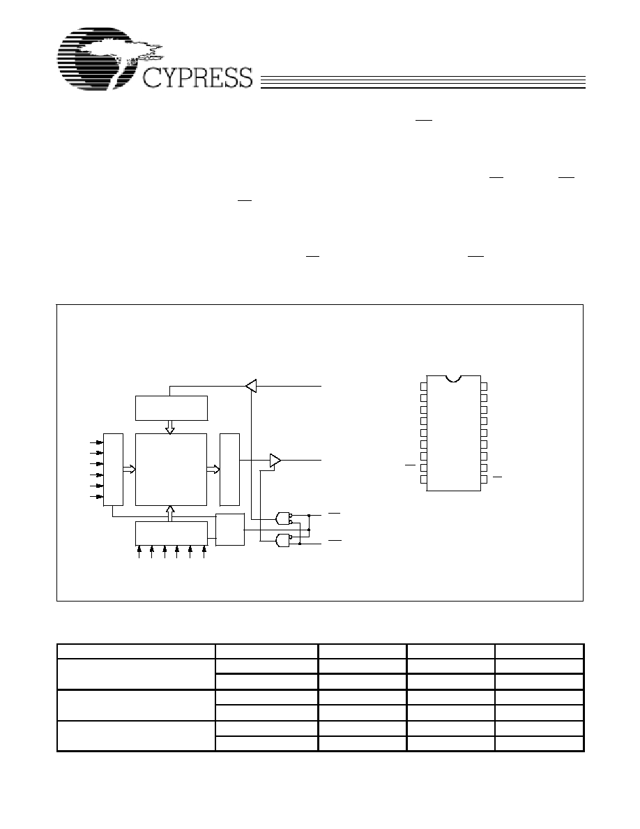
CY7C147
4K x 1 Static RAM
Features
D
Automatic power down when dese
lected
D
CMOS for optimum speed/power
D
High speed
25 ns
D
Low active power
440 mW (commercial)
605 mW (military)
D
Low standby power
55 mW
D
TTL compatible inputs and outputs
D
Capable of withstanding greater than
2001V electrostatic discharge
Functional Description
The CY7C147 is a high performance
CMOS static RAMs organized as 4096
words by 1 bit. Easy memory expansion is
provided by an active LOW chip enable
(CE) and three state drivers.
The
CY7C147 has an automatic power down
feature, reducing the power consumption
by 80% when deselected .
Writingtothedeviceisaccomplishedwhen
the chip select (CE) and write enable
(WE) inputs are both LOW. Data on the
input pin (DI) is written into the memory
location specified on the address pins (A
0
through A
11
).
Reading thedeviceisaccomplished bytak
ing the chip enable (CE) LOW while (WE)
remains HIGH. Under these conditions,
the contents of the location specified on
the address pins will appear on the data
output (DO) pin.
The output pin remains in a high impe
dance state when chip enable is HIGH, or
write enable (WE) is LOW.
Logic Block Diagram
Pin Configuration
64 x 64
ARRAY
Top View
DIP
A
1
A
2
A
3
A
8
A
9
A
6
A
0
COLUMN
DECODER
ROW
DECODER
SENSE
AMP
INPUT BUFFER
POWER
DOWN
WE
CE
DO
A
10
A
11
A
7
A
5
1
2
3
4
5
6
7
8
9
10
11
12
13
14
18
17
16
15
A
1
A
2
A
3
A
4
A
5
DO
CE
GND
WE
V
CC
A
6
A
7
A
8
A
0
A
9
A
10
A
11
DI
A
4
DI
C147 1
C147 2
Cypress Semiconductor Corporation
D
3901 North First Street
D
San Jose
D
CA 95134
D
408-943-2600
December 1985 - Revised November 1992
7c147: 12/4/89
Revision: Thursday, November 11, 1993
CY7C147
2
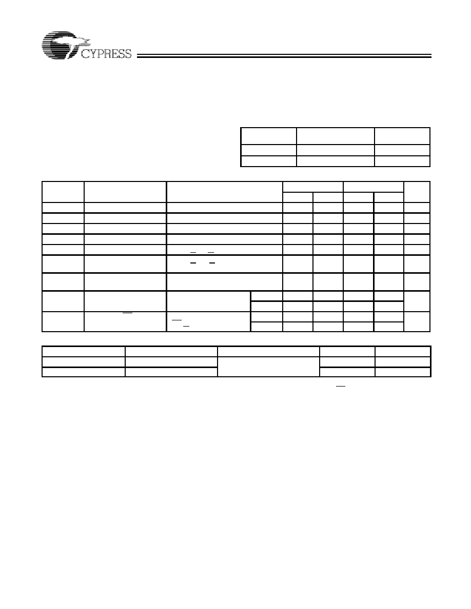
Maximum Ratings
(Above which the useful life may be impaired. For user guidelines,
not tested.)
Storage Temperature
-65
_
C to +150
_
C
. . . . . . . . . . . . . . . . . .
Ambient Temperature with
Power Applied
-55
_
C to +125
_
C
. . . . . . . . . . . . . . . . . . . . . . .
Supply Voltage to Ground Potential
(Pin 18 to Pin 9)
-0.5V to +7.0V
. . . . . . . . . . . . . . . . . . . . . . . .
DC Voltage Applied to Outputs
in High Z State
-0.5V to +7.0V
. . . . . . . . . . . . . . . . . . . . . . . . .
DC Input Voltage
-3.0V to +7.0V
. . . . . . . . . . . . . . . . . . . . . . .
Output Current into Outputs (LOW)
20 mA
. . . . . . . . . . . . . .
Static Discharge Voltage
>2001V
. . . . . . . . . . . . . . . . . . . . . . . .
(per MIL STD 883, Method 3015)
Latch Up Current
>200 mA
. . . . . . . . . . . . . . . . . . . . . . . . . . .
Operating Range
Range
Ambient
Temperature
V
CC
Commercial
0
_
C to +70
_
C
5V ± 10%
Military
[1]
-55
_
C to +125
_
C
5V ± 10%
Electrical Characteristics
Over the Operating Range
[2]
7C147-25
7C147-35, 45
Parameter
Description
Test Conditions
Min.
Max.
Min.
Max.
Unit
V
OH
Output High Voltage
V
CC
= Min., I
OH
= -4.0 mA
2.4
2.4
V
V
OL
Output Low Voltage
V
CC
= Min., I
OL
= 12.0 mA
0.4
0.4
V
V
IH
Input High Voltage
2.0
6.0
2.0
6.0
V
V
IL
Input Low Voltage
-3.0
0.8
-3.0
0.8
V
I
IX
Input Load Current
GND < V
I
< V
CC
-10
+10
-10
+10
mA
I
OZ
Output Leakage
Current
GND < V
O
< V
CC
Output Disabled
-50
+50
-50
+50
mA
I
OS
Output Short
Circuit Current
[3]
V
CC
= Max., V
OUT
= GND
-350
-350
mA
I
CC
V
CC
Operating
S
l C
t
V
CC =
Max.,
I
0 A
Com'l
90
80
mA
CC
p
g
Supply Current
CC =
,
I
OUT
= 0 mA
Mil
110
I
SB
Automatic CE
[4]
P
D
C
t
Max. V
CC
,
CE
V
Com'l
15
10
mA
Power Down Current
CC
,
CE > V
IH
Mil
10
Capacitance
[5]
Parameter
Description
Test Conditions
Max.
Unit
C
IN
Input Capacitance
T
A
= 25
_
C, f = 1 MHz,
5
8
pF
C
OUT
Output Capacitance
T
A
25 C, f
1 MHz,
V
CC
= 5.0V
8
pF
Notes:
1. T
A
is the "instant on" case temperature.
2. See the last page of this specification for Group A subgroup testing
information.
3. Duration of the short circuit should not exceed 30 seconds.
4. A pull up resistor to V
CC
on the CE input is required to keep the de
vice deselected during VCC power up, otherwise I
SB
will exceed values
given.
5. Tested initially and after any design or process changes that may af
fect these parameters.
7c147: 12/4/89
Revision: Thursday, November 11, 1993
CY7C147
3
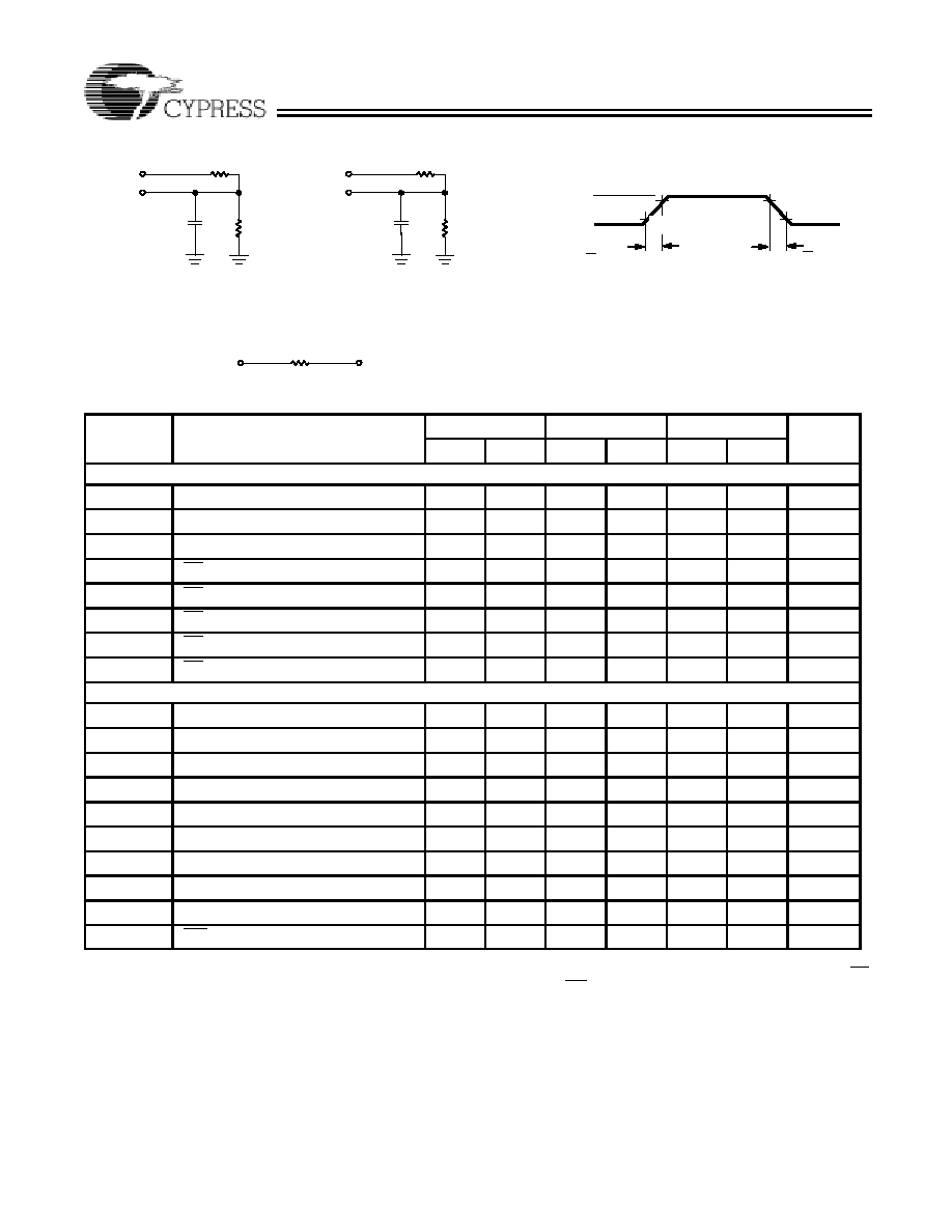
AC Test Loads and Waveforms
3.0V
5V
OUTPUT
R1 329W
R2
255W
30 pF
INCLUDING
JIG AND
SCOPE
GND
90%
10%
90%
10%
< 5 ns
< 5 ns
5V
OUTPUT
R1 329W
R2
255W
5 pF
INCLUDING
JIG AND
SCOPE
(a)
(b)
OUTPUT
1.90V
Equivalent to:
THÉVENIN EQUIVALENT
ALL INPUT PULSES
125W
C147 3
C147 4
Switching Characteristics
Over the Operating Range
[6]
7C147-25
7C147-35
7C147-45
Parameter
Description
Min.
Max.
Min.
Max.
Min.
Max.
Unit
READ CYCLE
t
RC
Read Cycle Time
25
35
45
ns
t
AA
Address to Data Valid
25
35
45
ns
t
OHA
Data Hold from Address Change
3
5
5
ns
t
ACE
CE LOW to Data Valid
25
35
45
ns
t
LZCE
CE LOW to Low Z
[7]
5
5
5
ns
t
HZCE
CE HIGH to High Z
[7, 8]
20
30
30
ns
t
PU
CE LOW to Power Up
0
0
0
ns
t
PD
CE HIGH to Power Down
20
20
20
ns
WRITE CYCLE
[9]
t
WC
Write Cycle Time
25
35
45
ns
t
SCE
CE LOW to Write End
25
35
45
ns
t
AW
Address Set Up to Write End
25
35
45
ns
t
HA
Address Hold from Write End
0
0
0
ns
t
SA
Address Set Up to Write Start
0
0
0
ns
t
PWE
WE Pulse Width
15
20
25
ns
t
SD
Data Set Up to Write End
15
20
25
ns
t
HD
Data Hold from Write End
0
10
10
ns
t
LZWE
WE HIGH to Low Z
[7]
0
0
0
ns
t
HZWE
WE LOW to High Z
[7, 8]
15
20
25
ns
Notes:
6. Test conditions assume signal transition times of 5 ns or less, timing
reference levels of 1.5V, input pulse levels of 0 to 3.0V, and output
loading of the specified I
OL
/I
OH
and 30 pF load capacitance.
7. At any given temperature and voltage condition, t
HZ
is less than t
LZ
for all devices.
8. t
HZCE
and t
HZWE
are tested with C
L
= 5 pF as in part (b) of AC Test
Loads. Transition is measured ±500 mV from steady state voltage.
9. The internal write time of the memory is defined by the overlap of CE
LOW and WE LOW. Both signals must be LOW to initiate a write
and either signal can terminate a write by going HIGH. The data in
put set up and hold timing should be referenced to the rising edge of
the signal that terminates the write.
7c147: 12/4/89
Revision: Thursday, November 11, 1993
CY7C147
4
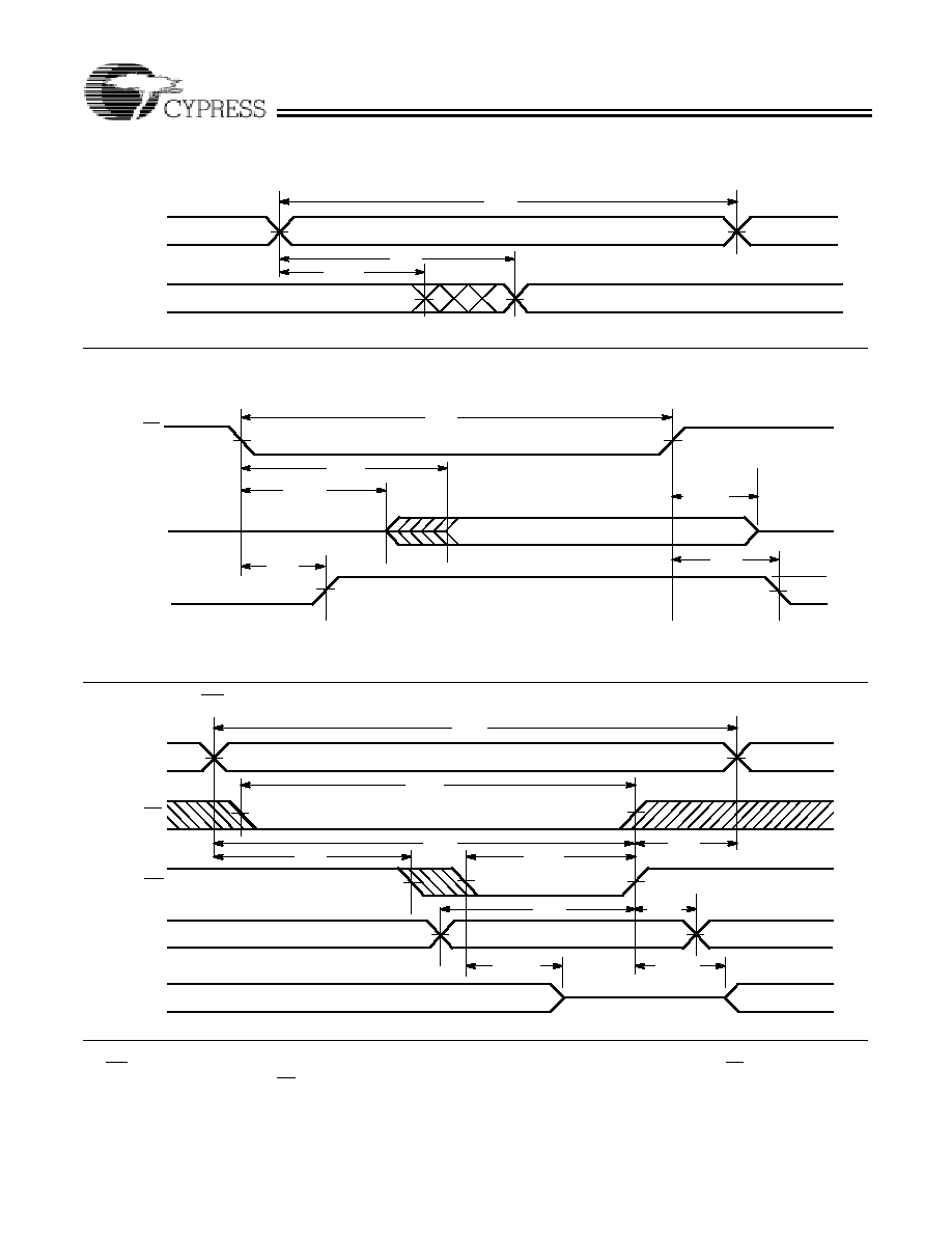
Switching Waveforms
Read Cycle No. 1
[10, 11]
Read Cycle No. 2
[10, 12]
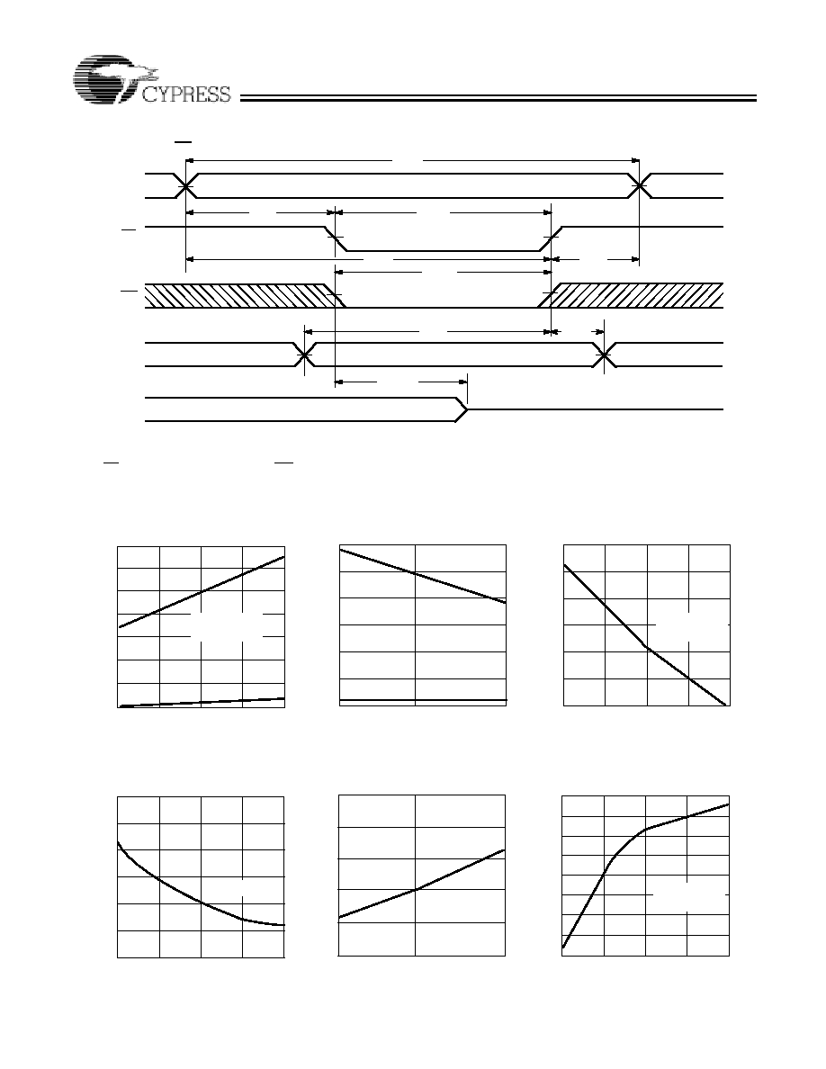
Write Cycle No. 1 (WE Controlled)
[9]
ADDRESS
50%
DATA OUT
PREVIOUS DATA VALID
DATA VALID
t
RC
t
AA
50%
DATA VALID
t
RC
t
ACE
t
LZCE
t
PU
DATA OUT
HIGH IMPEDANCE
IMPEDANCE
ICC
ISB
t
HZCE
t
PD
CE
HIGH
t
WC
DATA UNDEFINED
HIGH IMPEDANCE
t
SCE
t
AW
t
SA
t
PWE
t
HA
t
HD
V
CC
SUPPLY
CURRENT
t
HZWE
t
LZWE
t
SD
CE
WE
DATA IN
DATA OUT
ADDRESS
t
OHA
C147 5
C147 6
C147 7
DATA
IN
VALID
Notes:
10. WE is HIGH for read cycle.
11. Device is continuously selected, CE = V
IL
.
12. Address valid prior to or coincident with CE transition LOW.
7c147: 12/4/89
Revision: Thursday, November 11, 1993
CY7C147
5
Switching Waveforms
(continued)
Write Cycle No. 2 (CE Controlled)
[9, 13]
t
WC
DATA UNDEFINED
HIGH IMPEDANCE
t
SCE
t
AW
t
PWE
t
HA
t
HD
t
HZWE
t
SD
ADDRESS
CE
WE
DATA IN
DATA OUT
t
SA
C147 8
DATA
IN
VALID
Notes:
13. If CE goes HIGH simultaneously with WE HIGH, the output re
mainsin a high impedance state.
Typical DC and AC Characteristics
1.2
1.4
1.0
0.6
0.4
0.2
4.0
4.5
5.0
5.5
6.0
1.6
1.4
1.2
1.0
0.8
-55
25
125
-55
25
125
1.2
1.0
0.8
NORMALIZED
t
AA
120
100
80
60
40
20
0.0
1.0
2.0
3.0
4.0
OUTPUT
SOURCE
CURRENT
(mA)
SUPPLY VOLTAGE (V)
NORMALIZED SUPPLY CURRENT
vs. SUPPLY VOLTAGE
NORMALIZED ACCESS TIME
vs. AMBIENT TEMPERATURE
AMBIENT TEMPERATURE (_C)
NORMALIZED SUPPLY CURRENT
vs. AMBIENT TEMPERATURE
AMBIENT TEMPERATURE (_C)
OUTPUT VOLTAGE (V)
OUTPUT SOURCE CURRENT
vs. OUTPUT VOLTAGE
0.0
0.8
1.4
1.1
1.0
0.9
4.0
4.5
5.0
5.5
6.0
NORMALIZED
t
SUPPLY VOLTAGE (V)
NORMALIZED ACCESS TIME
vs. SUPPLY VOLTAGE
120
140
100
60
40
20
0.0
1.0
2.0
3.0
4.0
OUTPUT
SINK
CURRENT
(mA)
0
80
OUTPUT VOLTAGE (V)
OUTPUT SINK CURRENT
vs. OUTPUT VOLTAGE
0.6
0.4
0.2
0.0
NORMALIZED
I
,
I
CC
SB
NORMALIZED
I
,
I
CC
SB
I
SB
V
CC
= 5.0V
V
IN
= 5.0V
I
CC
I
CC
V
CC
= 5.0V
V
CC
= 5.0V
T
A
= 25_C
V
CC
= 5.0V
T
A
= 25_C
I
SB
T
A
= 25_C
0.6
0.8
0
AA
1.3
1.2
V
IN
= 5.0V
T
A
= 25_C
160