PRELIMINARY
2M x 36/4M x 18/1M x 72 Flow-through
SRAM with NoBLTM Architecture
CY7C1471V33
CY7C1473V33
CY7C1475V33
Cypress Semiconductor Corporation
∑
3901 North First Street
∑
San Jose
,
CA 95134
∑
408-943-2600
Document #: 38-05288 Rev. *A
Revised January 27, 2003
Features
∑ Zero Bus Latency, no dead cycles between Write and
Read cycles
∑ Supports 133-MHz bus operations
∑ 2M ◊ 36/4M ◊ 18/1M ◊ 72 common I/O
∑ Fast clock-to-output times
-- 5.5 ns (for 150-MHz device)
-- 6.5 ns (for 133-MHz device)
-- 7.5 ns (for 117-MHz device)
-- 8.5 ns (for 100-MHz device)
∑ Single 3.3V ≠5% and +5% power supply V
DD
∑ Separate V
DDQ
for 3.3V or 2.5V
∑ Clock Enable (CEN) pin to suspend operation
∑ Burst Capability≠linear or interleaved burst order
∑ Available in 119-ball bump BGA and 100-pin TQFP
packages (CY7C1471V33 and CY7C1473V33)
∑ 165-ball FBGA and 209-ball BGA(CY7C1475V33)
packages are offered by opportunity basis. (Please
contact Cypress sales or marketing
Functional Description
The CY7C1471V33, CY7C1473V33, and CY7C1475V33
SRAMs are designed to eliminate dead cycles when transi-
tions from Read to Write or vice versa. These SRAMs are
optimized for 100 percent bus utilization and achieves Zero
Bus Latency. They integrate 2,097,152 ◊ 36/4,194,304 ◊ 18/
1,048,576 ◊ 72 SRAM cells, respectively, with advanced
synchronous peripheral circuitry and a two-bit counter for
internal burst operation. The Synchronous Burst SRAM family
employs high-speed, low-power CMOS designs using
advanced single layer polysilicon, three-layer metal
technology. Each memory cell consists of six transistors.
All synchronous inputs are gated by registers controlled by a
positive-edge-triggered Clock Input (CLK). The synchronous
inputs include all addresses, all data inputs, depth-expansion
Chip Enables (CE
1
, CE
2
,
and CE
3
), cycle start input (ADV/LD),
Clock Enable (CEN), Byte Write Selects (BWS
a
, BWS
b
,
BWS
c
, BWS
d
, BWS
e
, BWS
f
, BWS
g
, BWS
h
), and Read-Write
control (WE). BWS
c
and BWS
d
apply to CY7C1471V33 and
CY7C1475V33 only. BWS
e
, BWS
f
, BWS
g
, and BWS
h
apply to
CY7C1475V33 only.
A Clock Enable (CEN) pin allows operation of the
CY7C1471V33, CY7C1473V33, and CY7C1475V33 to be
suspended as long as necessary. All synchronous inputs are
ignored when (CEN) is HIGH and the internal device registers
will hold their previous values.
There are three Chip Enable (CE
1
, CE
2
, CE
3
) pins that allow
the user to deselect the device when desired. If any one of
these three are not active when ADV/LD is LOW, no new
memory operation can be initiated and any burst cycle in
progress is stopped. However, any pending data transfers
(Read or Write) will be completed. The data bus will be in
high-impedance state two cycles after chip is deselected or a
Write cycle is initiated.
The CY7C1471V33, CY7C1473V33, and CY7C1475V33
have an on-chip two-bit burst counter. In the burst mode,
CY7C1471V33, CY7C1473V33, and CY7C1475V33 provide
four cycles of data for a single address presented to the
SRAM. The order of the burst sequence is defined by the
MODE input pin. The MODE pin selects between linear and
interleaved burst sequences. The ADV/LD signal is used to
load a new external address (ADV/LD = LOW) or increment
the internal burst counter (ADV/LD = HIGH).
Output Enable (OE) and burst sequence select (MODE) are
the asynchronous signals. OE can be used to disable the
outputs at any given time. ZZ may be tied to LOW if it is not
used.
Four pins are used to implement JTAG test capabilities. The
JTAG circuitry is used to serially shift data to and from the
device. JTAG inputs use LVTTL/LVCMOS levels to shift data
during this testing mode of operation.
CLK
A
x
CEN
WE
BWS
x
CE1
CE
CE2
OE
2M ◊ 36/
MEMORY
ARRAY
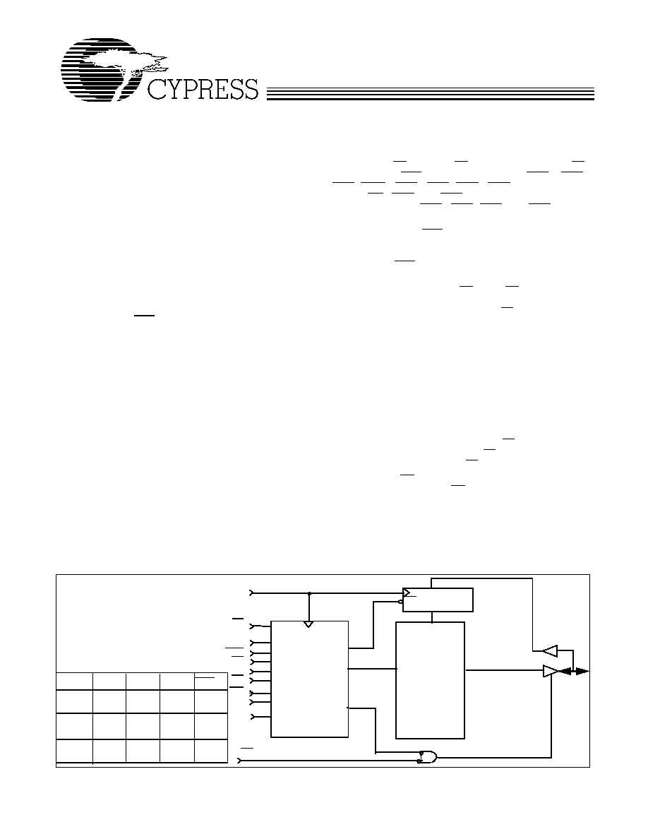
Logic Block Diagram
DQ
x
Data-In REG.
Q
D
CE
CONTROL
and Write
LOGIC
3
ADV/LD
Mode
DP
x
4M ◊ 18/
1M ◊ 72
2M ◊ 36
4M ◊ 18
A
X
DQ
X
DP
X
BWS
X
X = 20:0
X = 21:0 X = a, b
X= a, b,
1M ◊ 72
X = 19:0
X = a, b,
c, d
X = a, b,
c, d
c, d
X = a, b
X = a, b
X = a, b,
c,d,e,f,g,h
X = a, b,
c,d,e,f,g,h c,d,e,f,g,h
X = a, b,
PRELIMINARY
CY7C1471V33
CY7C1473V33
CY7C1475V33
Document #: 38-05288 Rev. *A
Page 2 of 26
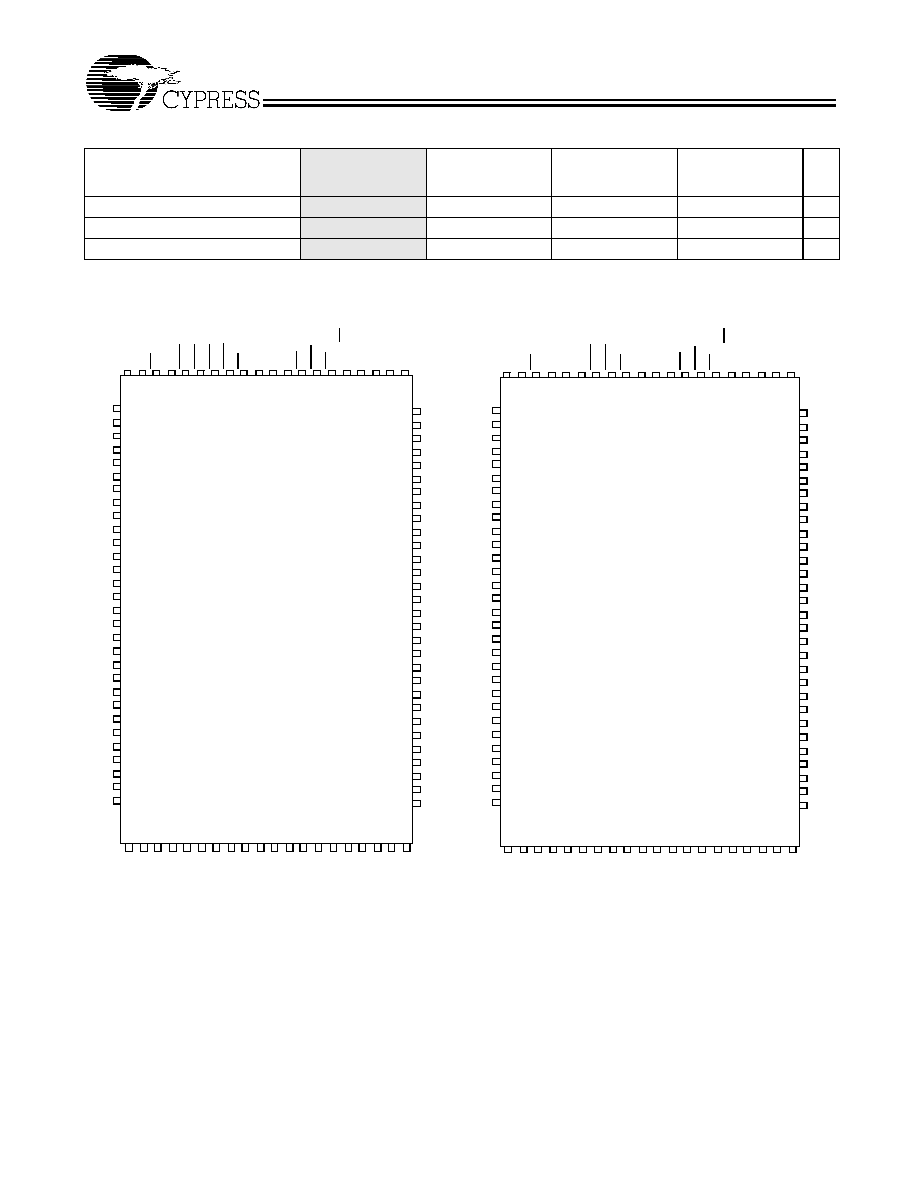
Pin Configurations
Selection Guide
CY7C1471V33-150
CY7C1473V33-150
CY7C1475V33-150
CY7C1471V33-133
CY7C1473V33-133
CY7C1475V33-133
CY7C1471V33-117
CY7C1473V33-117
CY7C1475V33-117
CY7C1471V33-100
CY7C1473V33-100
CY7C1475V33-100 Unit
Maximum Access Time
5.5
6.5
7.5
8.5
ns
Maximum Operating Current
TBD
TBD
TBD
TBD
mA
Maximum CMOS Standby Current
TBD
TBD
TBD
TBD
mA
Shaded area contains advanced information.
A
A
A
A
A
1
A
0
NC
NC
V
SS
V
DD
A
A
A
A
A
A
V
DDQ
V
SS
DQb
DQb
DQb
V
SS
V
DDQ
DQb
DQb
V
SS
NC
V
DD
DQa
DQa
V
DDQ
V
SS
DQa
DQa
V
SS
V
DDQ
V
DDQ
V
SS
DQc
DQc
V
SS
V
DDQ
DQc
DQc
V
DD
V
SS
DQd
DQd
V
DDQ
V
SS
DQd
DQd
DQd
V
SS
V
DDQ
A
A
CE
1
CE
2
BW
S
a
CE
3
V
DD
V
SS
CL
K
WE
CEN
OE
A
A
1
2
3
4
5
6
7
8
9
10
11
12
13
14
15
16
17
18
19
20
21
22
23
24
25
26
27
28
29
30
31
32
33
34
35
36
37
38
39
40
41
42
43
44
45
46
47
48
49
50
80
79
78
77
76
75
74
73
72
71
70
69
68
67
66
65
64
63
62
61
60
59
58
57
56
55
54
53
52
51
100
99
98
97
96
95
94
93
92
91
90
89
88
87
86
85
84
83
82
81
A
A
ADV/
L
D
ZZ
CY7C1471V33
100-pin TQFP Packages
A
A
A
A
A
1
A
0
NC
NC
V
SS
V
DD
A
A
A
A
A
A
A
NC
NC
V
DDQ
V
SS
NC
DPa
DQa
DQa
V
SS
V
DDQ
DQa
DQa
V
SS
NC
V
DD
DQa
DQa
V
DDQ
V
SS
DQa
DQa
NC
NC
V
SS
V
DDQ
NC
NC
NC
NC
NC
NC
V
DDQ
V
SS
NC
NC
DQb
DQb
V
SS
V
DDQ
DQb
DQb
NC
V
DD
V
SS
DQb
DQb
V
DDQ
V
SS
DQb
DQb
DPb
NC
V
SS
V
DDQ
NC
NC
NC
A
A
CE
1
CE
2
NC
NC
BW
S
b
BW
S
a
CE
3
V
DD
V
SS
CL
K
WE
CE
N
OE
A
A
A
1
2
3
4
5
6
7
8
9
10
11
12
13
14
15
16
17
18
19
20
21
22
23
24
25
26
27
28
29
30
31
32
33
34
35
36
37
38
39
40
41
42
43
44
45
46
47
48
49
50
80
79
78
77
76
75
74
73
72
71
70
69
68
67
66
65
64
63
62
61
60
59
58
57
56
55
54
53
52
51
10
0
99
98
97
96
95
94
93
92
91
90
89
88
87
86
85
84
83
82
81
A
A
AD
V/LD
ZZ
MO
DE
A
BW
S
d
MO
DE
BW
S
c
DQc
DQc
DQc
DQc
DPc
DQd
DQd
DPd
DQd
NC
DPb
DQb
DQa
DQa
DQa
DQa
DPa
DQb
DQb
(2M ◊ 36)
CY7C1473V33
BW
S
b
NC
NC
A
A
A
A
(4M ◊ 18)