Äîêóìåíòàöèÿ è îïèñàíèÿ www.docs.chipfind.ru
1Kx4 Static RAM
CY7C150
Cypress Semiconductor Corporation
·
3901 North First Street
·
San Jose
·
CA 95134
·
408-943-2600
Document #: 38-05024 Rev. **
Revised August 24, 2001
50
Features
· Memory reset function
· 1024 x 4 static RAM for control store in high-speed com-
puters
· CMOS for optimum speed/power
· High speed
-- 10 ns (commercial)
-- 12 ns (military)
· Low power
-- 495 mW (commercial)
-- 550 mW (military)
· Separate inputs and outputs
· 5-volt power supply
±
10% tolerance in both commercial
and military
· Capable of withstanding greater than 2001V static dis-
charge
· TTL-compatible inputs and outputs
Functional Description
The CY7C150 is a high-performance CMOS static RAM de-
signed for use in cache memory, high-speed graphics, and
data-acquisition applications. The CY7C150 has a memory re-
set feature that allows the entire memory to be reset in two
memory cycles.
Separate I/O paths eliminates the need to multiplex data in
and data out, providing for simpler board layout and faster sys-
tem performance. Outputs are three-stated during write, reset,
deselect, or when output enable (OE) is held HIGH, allowing
for easy memory expansion.
Reset is initiated by selecting the device (CS = LOW) and tak-
ing the reset (RS) input LOW. Within two memory cycles all
bits are internally cleared to zero. Since chip select must be
LOW for the device to be reset, a global reset signal can be
employed, with only selected devices being cleared at any giv-
en time.
Writing to the device is accomplished when the chip select
(CS) and write enable (WE) inputs are both LOW. Data on the
four data inputs (D
0
-
D
3
) is written into the memory location
specified on the address pins (A
0
through A
9
).
Reading the device is accomplished by taking chip select (CS)
and output enable (OE) LOW while write enable (WE) remains
HIGH. Under these conditions, the contents of the memory
location specified on the address pins will appear on the four
output pins (O
0
through O
3
).
The output pins remain in high-impedance state when chip
enable (CE) or output enable (OE) is HIGH, or write enable
(WE) or reset (RS) is LOW.
A die coat is used to insure alpha immunity.
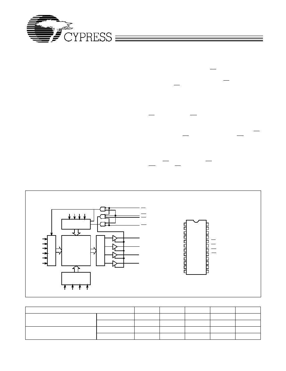
Logic Block Diagram
Pin Configuration
C1501
64 x 64
ARRA
Y
A
0
A
1
A
2
A
3
A
4
COLUMNDECODER
ROW
D
E
CODE
R
S
E
N
S
E AM
PS
DATAINPUT
CONTROL
O
0
O
1
O
2
O
3
A
6
A
7
A
8
D
0
D
1
D
2
D
3
COLUMN
DECODER
OE
WE
CS
RS
1
2
3
4
5
6
7
8
9
10
11
12
13
14
18
17
16
15
19
22
21
20
Top View
DIP/SOIC
7C150
A3
A4
A5
A6
A7
O2
VCC
A2
WE
CS
OE
O3
D2
D3
C150-2
A8
A9
D0
O0
D1
23
24
A1
A0
RS
O1
GND
A
5
A
9
Selection Guide
7C150
-
10
7C150
-
12
7C150
-
15
7C150
-
25
7C150
-
35
Maximum Access Time (ns)
Commercial
10
12
15
25
Military
12
15
25
35
Maximum Operating Current (mA)
Commercial
90
90
90
90
90
Military
100
100
100
100
CY7C150
Document #: 38-05024 Rev. **
Page 2 of 11
Maximum Ratings
(Above which the useful life may be impaired. For user guide-
lines, not tested.)
Storage Temperature
......................................-
65
°
C to+150
°
C
Ambient Temperature with
Power Applied
...................................................-
55
°
C to+125
°
C
Supply Voltage to Ground Potential
(Pin 24 to Pin 12)
..................................................-
0.5V to+7.0V
DC Voltage Applied to Outputs
in High Z State
......................................................-
0.5V to+7.0V
DC Input Voltage
.................................................-
3.0V to +7.0V
Output Current into Outputs (LOW) .............................20 mA
Static Discharge Voltage .......................................... >2001V
(per MIL-STD-883, Method 3015)
Latch-Up Current .................................................... >200 mA
Operating Range
Range
Ambient
Temperature
V
CC
Commercial
0
°
C to +70
°
C
5V
±
10%
Military
[1]
-
55
°
C to +125
°
C
5V
±
10%
Note:
1.
T
A
is the "instant on" case temperature.
Electrical Characteristics
Over the Operating Range
[2]
Parameter
Description
Test Conditions
7C150
Unit
Min.
Max.
V
OH
Output HIGH Voltage
V
CC
= Min., I
OH
=
-
0.4 mA
2.4
V
V
OL
Output LOW Current
V
CC
= Min., I
OL
= 12 mA
0.4
V
V
IH
Input HIGH Level
2.0
V
CC
V
V
IL
Input LOW Level
-
3.0
0.8
V
I
IX
Input Load Current
GND < V
I
< V
CC
-
10
+10
µ
A
I
OZ
Output Current (High Z)
V
OL
< V
OUT
< V
OH
,
Output Disabled
-
50
+50
µ
A
I
OS
Output Short Circuit Current
[3]
V
CC
= Max., V
OUT
= GND
-
300
mA
I
CC
V
CC
Operating Supply Current
V
CC
= Max.,
I
OUT
= 0 mA
Commercial
90
mA
Military
100
mA
Notes:
2.
See the last page of this specification for Group A subgroup testing information.
3.
Not more than 1 output should be shorted at a time. Duration of the short circuit should not exceed 30 seconds.
Capacitance
[4]
Parameter
Description
Test Conditions
Max.
Unit
C
IN
Input Capacitance
T
A
= 25
°
C, f = 1 MHz,
V
CC
= 5.0V
10
pF
C
OUT
Output Capacitance
10
pF
Note:
4.
Tested initially and after any design or process changes that may affect these parameters.
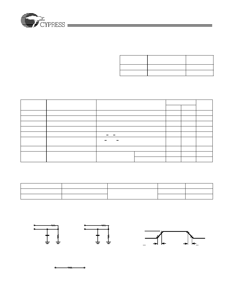
AC Test Loads and Waveforms
3.0V
5V
OUTPUT
R1329
R2
202
30 pF
GND
90%
90%
10%
< 3 ns
< 3 ns
5V
OUTPUT
C1503
R2
202
5 pF
C1504
OUTPUT
1.9V
INCLUDING
JIG AND
SCOPE
INCLUDING
JIG AND
SCOPE
R1329
Equivalent to:
THÉ VENIN EQUIVALENT
10%
ALL INPUT PULSES
(a)
(b)
125
CY7C150
Document #: 38-05024 Rev. **
Page 3 of 11
Switching Characteristics
Over the Operating Range
[2,5]
Parameter
Description
7C150
-
10
7C150
-
12
7C150
-
15
7C150
-
25
7C150
-
35
Unit
Min.
Max.
Min.
Max.
Min.
Max.
Min.
Max.
Min.
Max.
READ CYCLE
t
RC
Read Cycle Time
10
12
15
25
35
ns
t
AA
Address to Data Valid
10
12
15
25
35
ns
t
OHA
Output Hold from Address
Change
2
2
2
2
2
ns
t
ACS
CS LOW to Data Valid
8
10
12
15
20
ns
t
LZCS
CS LOW to Low Z
[6]
0
0
0
0
0
ns
t
HZCS
CS HIGH to High Z
[6,7]
6
8
11
20
25
ns
t
DOE
OE LOW to Data Valid
6
8
10
15
20
ns
t
LZOE
OE LOW to Low Z
[6]
0
0
0
0
0
ns
t
HZOE
OE HIGH to High Z
[6,7]
6
8
9
20
25
ns
WRITE CYCLE
[8]
t
WC
Write Cycle Time
10
12
15
25
35
ns
t
SCS
CS LOW to Write End
6
8
11
15
20
ns
t
AW
Address Set-Up to Write End
8
10
13
20
30
ns
t
HA
Address Hold from Write End
2
2
2
5
5
ns
t
SA
Address Set-Up to Write Start
2
2
2
5
5
ns
t
PWE
WE Pulse Width
6
8
11
15
20
ns
t
SD
Data Set-Up to Write End
6
8
11
15
20
ns
t
HD
Data Hold from Write End
2
2
2
5
5
ns
t
LZWE
WE HIGH to Low Z
[6]
0
0
0
0
0
ns
t
HZWE
WE LOW to High Z
[6,7]
6
8
12
20
25
ns
RESET CYCLE
t
RRC
Reset Cycle Time
20
24
30
50
70
ns
t
SAR
Address Valid to Beginning of
Reset
0
0
0
0
0
ns
t
SWER
Write Enable HIGH to Beginning
of Reset
0
0
0
0
0
ns
t
SCSR
Chip Select LOW to Beginning of
Reset
0
0
0
0
0
ns
t
PRS
Reset Pulse Width
10
12
15
20
30
ns
t
HCSR
Chip Select Hold After End of
Reset
0
0
0
0
0
ns
t
HWER
Write Enable Hold After End of
Reset
8
12
15
30
40
ns
t
HAR
Address Hold After End of Reset
10
12
15
30
40
ns
t
LZRS
Reset HIGH to Output in Low Z
[6]
0
0
0
0
0
ns
t
HZRS
Reset LOW to Output in
High Z
[6,7]
6
8
12
20
25
ns
Notes:
5.
Test conditions assume signal transition times of 5 ns or less, timing reference levels of 1.5V, input pulse levels of 0 to 3.0V, and output loading of the specified
I
OL
/I
OH
and 30-pF load capacitance.
6.
At any given temperature and voltage condition, t
HZ
is less than t
LZ
for any given device.
7.
t
HZCS
, t
HZOE
, t
HZR
, and t
HZWE
are tested with C
L
= 5 pF as in part (b) of AC Test Loads. Transition is measured
±
500 mV from steady-state voltage.
8.
The internal write time of the memory is defined by the overlap of CS LOW and WE LOW. Both signals must be LOW to initiate a write and either signal can terminate
a write by going HIGH. The data input set-up and hold timing should be reference to the rising edge of the signal that terminates the write.
CY7C150
Document #: 38-05024 Rev. **
Page 4 of 11
Switching Waveforms
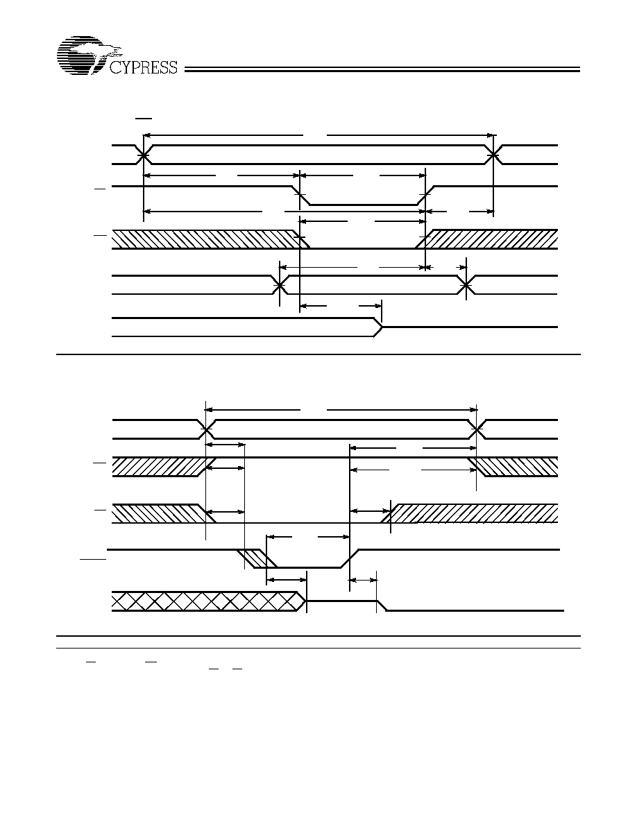
Notes:
9.
WE is HIGH for read cycle.
10. Device is continuously selected, CS and OE = V
IL
.
11. Address prior to or coincident with CS transition LOW.
Read Cycle No.1
ADDRESS
C150-5
DATA OUT
PREVIOUS DATA VALID
DATA VALID
t
RC
t
AA
t
OHA
[9,10]
Read Cycle No. 2
Write CycleNo.1 (WE Controlled)
DATA VALID
t
RC
t
ACS
t
DOE
t
LZOE
t
LZCS
DATA OUT
HIGH IMPEDANCE
IMPEDANCE
t
HZOE
t
HZCS
OE
CE
HIGH
C150-6
t
WC
DATA UNDEFINED
HIGH IMPEDANCE
t
SCS
t
AW
t
SA
t
PWE
t
HA
t
HD
t
HZWE
t
LZWE
t
SD
C150-7
CE
WE
DATA IN
DATA I/O
ADDRESS
DATA
IN
VALID
[9,11]
[8]
CY7C150
Document #: 38-05024 Rev. **
Page 5 of 11
Notes:
12. If CS goes HIGH with WE HIGH, the output remains in a high-impedance state.
13. Reset cycle is defined by the overlap of RS and CS for the minimum reset pulse width.
Switching Waveforms
(continued)
Write Cycle No.2 (CS Controlled)
t
WC
DATA UNDEFINED
HIGH IMPEDANCE
t
SCS
t
AW
t
SA
t
PWE
t
HA
t
HD
t
HZWE
t
SD
ADDRESS
CE
WE
DATA IN
DATA I/O
C150-8
DATA
IN
VALID
[8,12]
Reset Cycle
t
RRC
OUTPUT VALID ZERO
t
SAR
t
HCSR
t
HAR
t
LZRS
ADDRESS
WE
CS
DATA I/O
C150-9
t
PRS
HIGH
IMPEDANCE
t
HZRS
t
SWER
t
SCSR
RESET
t
HWER
[13]