/home/web/doc/html/cypress/169548
8Kx9 Static RAM
CY7C182
Cypress Semiconductor Corporation
·
3901 North First Street
·
San Jose
·
CA 95134
·
408-943-2600
October 4, 1999
Features
· High speed
-- t
AA
= 25 ns
· x9 organization is ideal for cache memory applications
· CMOS for optimum speed/power
· Low active power
-- 770 mW
· Low standby power
-- 195 mW
· TTL-compatible inputs and outputs
· Automatic power-down when deselected
· Easy memory expansion with CE
1
, CE
2
,
OE options
Functional Description
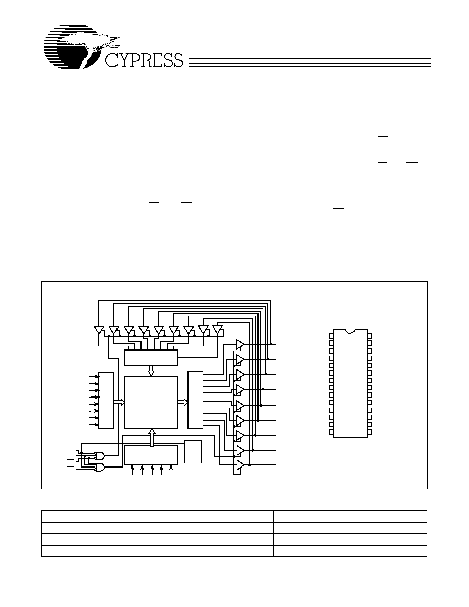
The CY7C182 is a high-speed CMOS static RAM organized
as 8,192 by 9 bits and it is manufactured using Cypress's high-
performance CMOS technology. Access times as fast as 25 ns
are available with maximum power consumption of only 770
mW.
The CY7C182, which is oriented toward cache memory appli-
cations, features fully static operation requiring no external
clocks or timing strobes. The automatic power-down feature
reduces the power consumption by more than 70% when the
circuit is deselected. Easy memory expansion is provided by
an active-LOW Chip Enable (CE
1
), an active HIGH Chip En-
able (CE
2
), an active-LOW Output Enable (OE), and three-
state drivers.
An active-LOW Write Enable signal (WE) controls the writ-
ing/reading operation of the memory. When CE
1
and WE in-
puts are both LOW, data on the nine data input/output pins
(I/O
0
through I/O
8
) is written into the memory location ad-
dressed by the address present on the address pins (A
0
through A
12
). Reading the device is accomplished by selecting
the device and enabling the outputs, (CE
1
and OE active LOW
and CE
2
active HIGH), while (WE) remains inactive or HIGH.
Under these conditions, the contents of the location addressed
by the information on address pins is present on the nine data
input/output pins.
The input/output pins remain in a high-impedance state unless
the chip is selected, outputs are enabled, and write enable
(WE) is HIGH.
A die coat is used to insure alpha immunity.
Logic Block Diagram
Pin Configuration
C1821
A
1
A
2
A
3
A
4
A
5
A
6
A
7
A
8
A
0
A
10
A
9
A
11
A
12
I/O
0
C1822
1
2
3
4
5
6
7
8
9
10
11
12
13
14
28
27
26
25
24
23
22
21
20
19
18
17
16
15
V
CC
WE
CE
2
A
3
A
2
A
1
OE
A
0
CE
1
I/O
8
I/O
7
I/O
6
I/O
5
I/O
4
A
4
A
5
A
6
A
7
A
8
A
9
A
10
A
11
A
12
I/O
0
I/O
1
I/O
2
I/O
3
GND
256 x 32 x 9
ARRAY
INPUT BUFFER
COLUMN
ROW
DE
CODE
R
SE
N
SE A
M
PS
POWER
DOWN
I/O
1
I/O
2
I/O
3
I/O
4
I/O
5
I/O
6
I/O
7
CE
1
CE
2
WE
OE
Top View
DIP/SOJ
I/O
8
DECODER
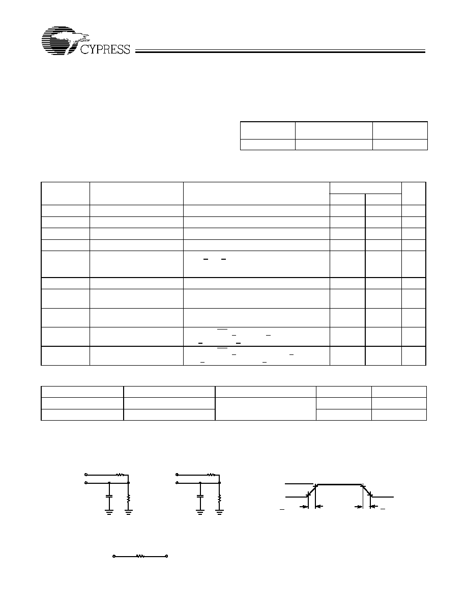
Selection Guide
7C182-25
7C182-35
7C182-45
Maximum Access Time (ns)
25
35
45
Maximum Operating Current (mA)
140
140
140
Maximum Standby Current (mA)
35
35
35
CY7C182
2
Maximum Ratings
(Above which the useful life may be impaired. For user guide-
lines, not tested.)
Storage Temperature
.....................................-
65
°
C to +150
°
C
Ambient Temperature with
Power Applied
..................................................-
55
°
C to +125
°
C
Supply Voltage to Ground Potential
[1]
..............-
0.5V to +7.0V
DC Voltage Applied to Outputs
in High Z State
[1]
.................................................-
0.5V to +7.0V
DC Input Voltage
[1]
..............................................-
0.5V to +7.0V
Output Current into Outputs (LOW) ............................. 20 mA
Static Discharge Voltage .......................................... >2001V
(per MIL-STD-883, Method 3015.2)
Latch-Up Current .................................................... >200 mA
Operating Range
Range
Ambient
Temperature
V
CC
Commercial
0
°
C to + 70
°
C
5V
±
10%
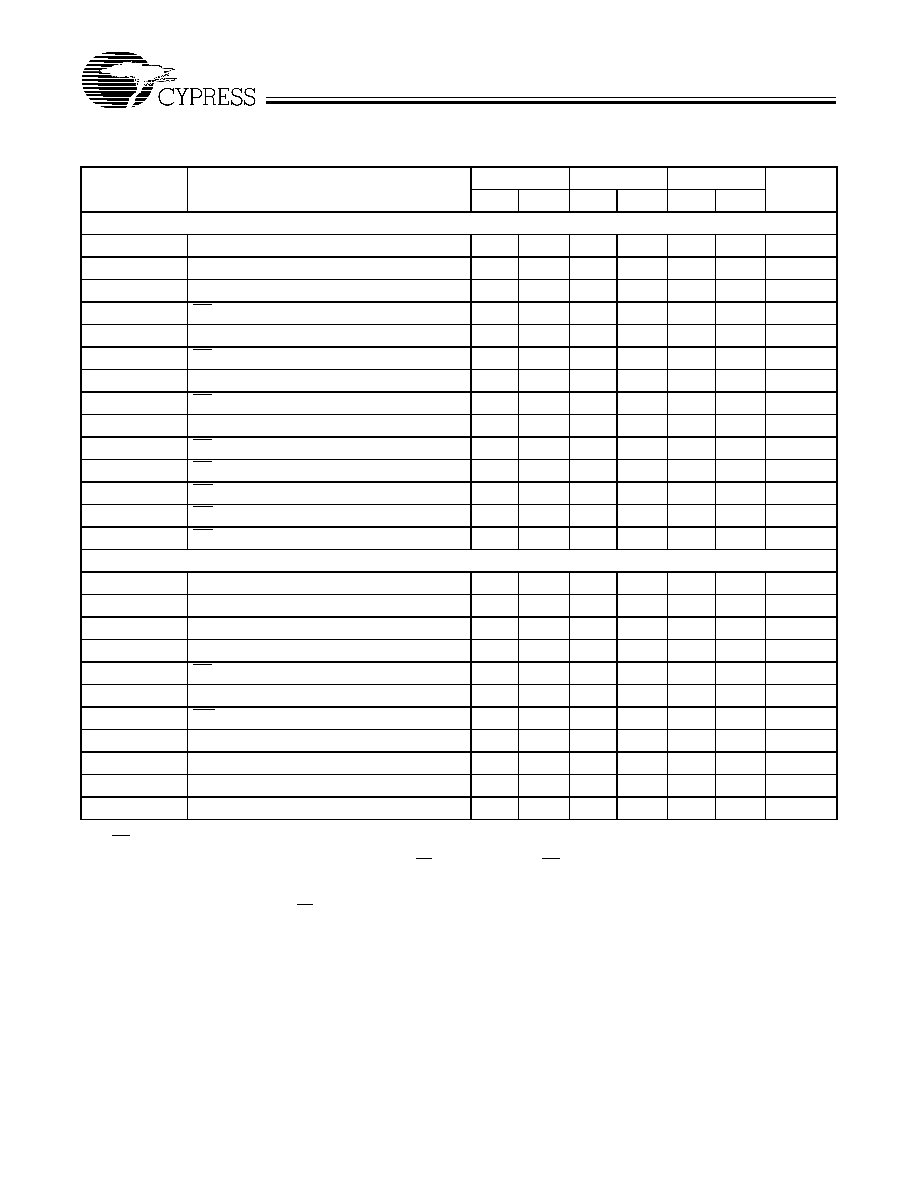
Electrical Characteristics
Over the Operating Range
Parameter
Description
Test Conditions
7C182-25, 35, 45
Min.
Max.
Unit
V
OH
Output HIGH Voltage
V
CC
Min., I
OH
=
-
4.0 mA.
2.4
V
V
OL
Output LOW Voltage
V
CC
Min., I
OL
= 8.0 mA
0.4
V
V
IH
Input HIGH Voltage
2.2
V
CC
V
V
IL
Input LOW Voltage
[1]
-
0.5
0.8
V
I
IX
Input Load Current
GND < V
IN
< V
CC
,
GND < V
OUT
< V
CC
,
Output Disabled
-
10
+10
µ
A
I
OZ
Output Leakage Current
V
CC
= Max., V
OUT
= GND
-
10
+10
µ
A
I
OS
Output Short Circuit
Current
[2]
V
CC
= Max., V
OUT
= GND
-
300
mA
I
CC
V
CC
Operating Circuit
Current
V
CC
Max., Output Current = 0 mA,
f = Max., V
IN
= V
CC
or GND
140
mA
Automatic Power-Down
Current -- TTL Inputs
Max V
CC
, CE
1
> V
IH
, CE
2
< V
IL
,
V
IN
> V
IH
or V
IN
< V
IL
, f = f
MAX
35
mA
Automatic Power-Down
Current -- CMOS Inputs
Max V
CC
, CE
1
> V
CC
-
0.3V, CE
2
< 0.3V,
V
IN
> V
CC
-
0.3V or V
IN
< 0.3V, f = 0
20
mA
Capacitance
[3]
Parameter
Description
Test Conditions
Max.
Unit
C
OUT
Output Capacitance
T
A
= 25
°
C, f = 1 MHz,
V
CC
= 5.0V
10
pF
C
IN
Input Capacitance
10
pF
Note:
1.
V
IL
(min.) =
-
3.0V for pulse durations of less than 20 ns.
2.
Duration of the short circuit should not exceed 30 seconds. Not more than one output should be shorted at one time.
3.
Tested initially and after any design or process changes that may affect these parameters.
AC Test Loads and Waveforms
3.0V
5V
OUTPUT
R1 481
R2
255
30 pF
INCLUDING
JIG AND
SCOPE
GND
90%
10%
90%
10%
< 5 ns
< 5 ns
5V
OUTPUT
R1 481
R2
255
5 pF
INCLUDING
JIG AND
SCOPE
(a)
(b)
OUTPUT
1.73V
Equivalent to:
THÉ VENIN EQUIVALENT
ALL INPUT PULSES
C1823
C1824
167
CY7C182
3
Switching Characteristics
Over the Operating Range
Parameter
Description
7C182-25
7C182-35
7C182-45
Unit
Min.
Max.
Min.
Max.
Min.
Max.
READ CYCLE
[4]
t
RC
Read Cycle Time
25
35
45
ns
t
AA
Address to Data Valid
25
35
45
ns
t
OHA
Data Hold from Address Change
3
3
3
ns
t
ACE1
CE
1
Access Time
25
35
45
ns
t
ACE2
CE
2
Access Time
25
35
45
ns
t
LZCE1
CE
1
LOW to Low Z
5
5
5
ns
t
LZCE2
CE
2
HIGH to Low Z
5
5
5
ns
t
HZCE1
CE
1
HIGH to High Z
[5]
18
20
25
ns
t
HZCE2
CE
2
LOW to High Z
[5]
18
20
25
t
PU
CE
1
LOW to Power-Up
0
0
0
ns
t
PD
CE
1
HIGH to Power-Down
20
20
25
ns
t
DOE
OE Access Time
18
20
20
ns
t
LZOE
OE LOW to Low Z
3
3
3
ns
t
HZOE
OE HIGH to High Z
[5]
18
20
25
ns
WRITE CYCLE
[6]
t
WC
Write Cycle Time
25
35
45
ns
t
SA
Address Set-Up Time
0
0
0
ns
t
AW
Address Valid to End of Write
20
30
40
ns
t
SD
Data Set-Up Time
15
20
25
ns
t
SCE1
CE
1
LOW to Write End
20
30
40
ns
t
SCE2
CE
2
HIGH to Write End
20
30
40
ns
t
PWE
WE Pulse Width
20
25
30
ns
t
HA
Address Hold from End of Write
0
0
0
ns
t
HD
Data Hold Time
0
0
0
ns
t
LZWE
Write HIGH to Low Z
[7]
3
3
3
ns
t
HZWE
Write LOW to High Z
[5, 7, 8]
13
15
20
ns
Notes:
4.
WE is HIGH for read cycle.
5.
t
HZCE
and t
HZWE
are specified with C
L
= 5 pF. Transition is measured
±
500 mV from steady-state voltage.
6.
The internal write time of the memory is defined by the overlap of CE
1
LOW, CE
2
HIGH, and WE LOW. All three signals must be asserted to initiate a write
and any signal can terminate a write by being deasserted. The data input set-up and hold timing should be referenced to the rising edge of the signal that
terminates the write.
7.
At any given temperature and voltage condition, t
LZWE
is less than t
HZWE
for any given device. These parameters are sampled and not 100% tested.
8.
Address valid prior to or coincident with CE transition LOW and CE
2
transition HIGH.
CY7C182
4
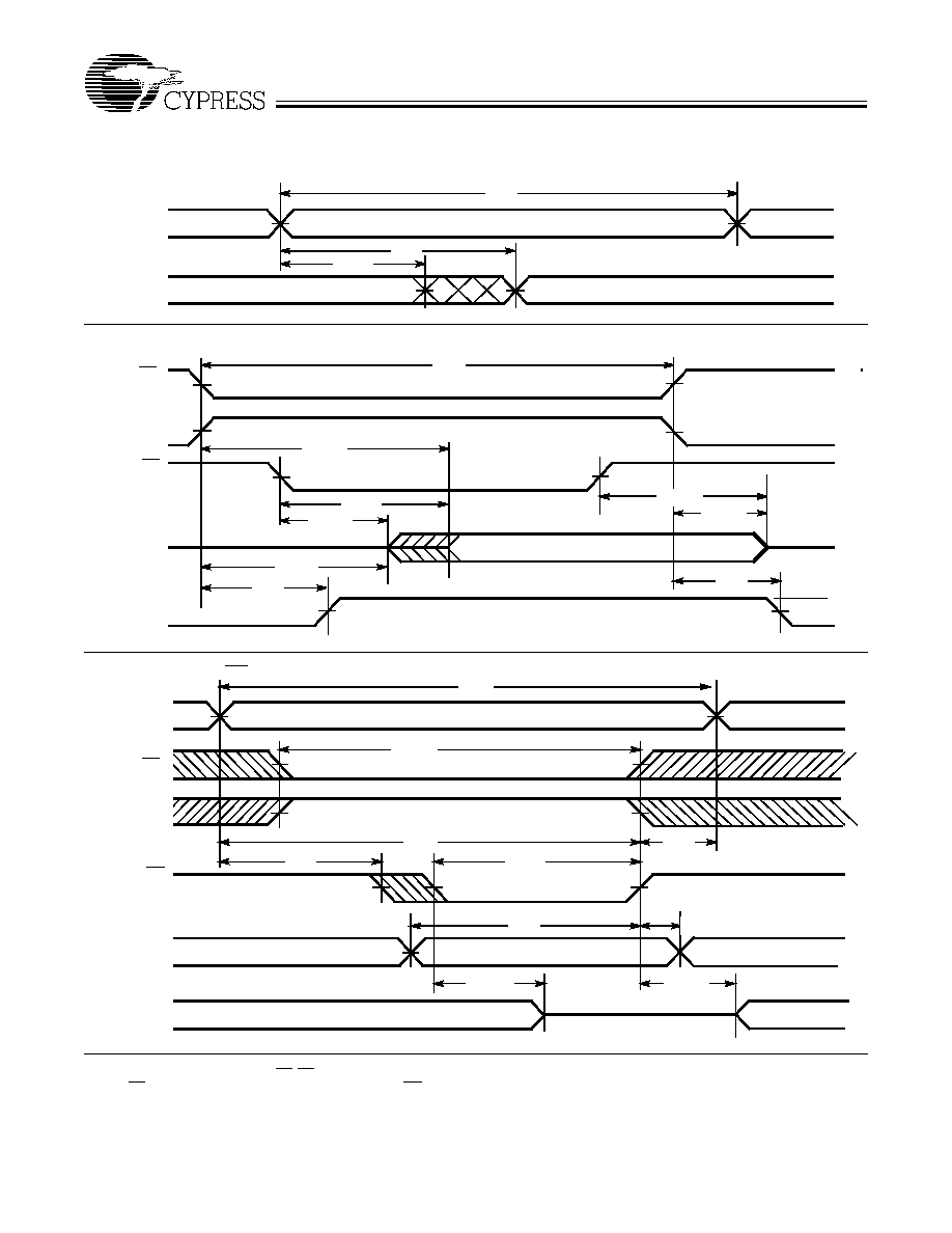
Switching Waveforms
Notes:
9.
Device is continuously selected. OE, CE
1
= V
IL
. CE
2
= V
IH.
10. If CE
1
goes HIGH and CE
2
goes LOW simultaneously with WE HIGH, the output remains in a high-impedance state.
Read Cycle
No. 1
ADDRESS
DATA OUT
PREVIOUS DATA VALID
DATA VALID
t
RC
t
AA
t
OHA
C1825
[4, 9]
Read Cycle No. 2
50%
50%
DATA VALID
t
RC
t
ACE1
t
ACE2
t
DOE
t
LZOE
t
LZCE
t
PU
HIGH IMPEDANCE
IMPEDANCE
ICC
ISB
t
HZOE
t
HZCE
t
PD
OE
HIGH
DATA OUT
V
CC
SUPPLY
CURRENT
CE
1
OE
CE
2
C1826
[4, 10]
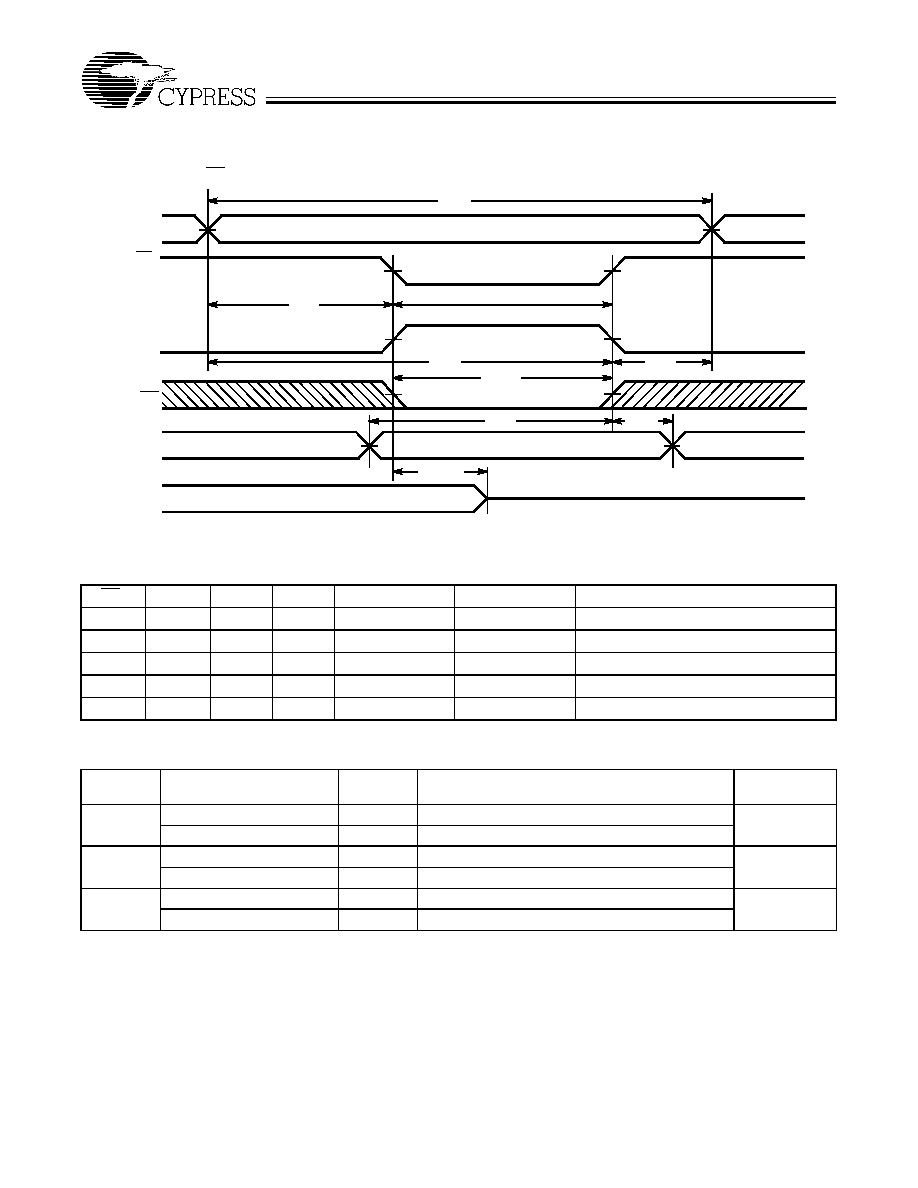
Write Cycle No. 1 (WE Controlled)
DATA VALID
DATA UNDEFINED
HIGH IMPEDANCE
t
HD
t
HZWE
t
SD
t
LZWE
t
PWE
t
SA
t
HA
t
AW
t
SCE1
t
SCE2
t
WC
DATA IN
DATA I/O
ADDRESS
CS
1
WE
CS
2
C1827
[6]
CY7C182
5
Document #: 38-00110-F
Switching Waveforms
(continued)
Write Cycle No. 2 (CE Controlled)
t
WC
DATA VALID
DATA UNDEFINED
HIGH IMPEDANCE
t
AW
t
SA
t
PWE
t
HA
t
HD
t
HZWE
t
SD
C1828
CE
2
WE
DATA IN
DATA I/O
ADDRESS
t
SCE1
CE
1
t
SCE2
[6, 10]
Truth Table
CE
1
CE
2
OE
WE
Data In
Data Out
Mode
H
X
X
X
Z
Z
Deselect/Power-Down
L
H
L
H
Z
Valid
Read
L
H
X
L
Valid
Z
Write
L
H
H
H
Z
Z
Output Disable
X
L
X
X
Z
Z
Deselect
Ordering Information
Speed
(ns)
Ordering Code
Package
Name
Package Type
Operating
Range
25
CY7C182
-
25PC
P21
28-Lead (300-Mil) Molded DIP
Commercial
CY7C182
-
25VC
V21
28-Lead Molded SOJ
35
CY7C182
-
35PC
P21
28-Lead (300-Mil) Molded DIP
Commercial
CY7C182
-
35VC
V21
28-Lead Molded SOJ
45
CY7C182
-
45PC
P21
28-Lead (300-Mil) Molded DIP
Commercial
CY7C182
-
45VC
V21
28-Lead Molded SOJ